 | –≠–ª–µ–∫—Ç—Ä–æ–Ω–Ω—ã–π –∫–æ–º–ø–æ–Ω–µ–Ω—Ç: CH1799TB | –°–∫–∞—á–∞—Ç—å:  PDF PDF  ZIP ZIP |
HIGH SPEED Modem and FAX FAMILY
CH2056/TBR/ETBR ≠ V.90 / 57,600bps/TBR21
CH1799/TBR/ETBR ≠ V.34bis / 33,600bps/TBR21
CH1794/TBR/ETBR ≠ V.32bis / 14,400bps/TBR21
2003 Cermetek Microelectronics, Inc.
Page 1
Document No. 607-0003 Revision K1 (06/03)
FEATURES
∑
Supports V.90, V.34bis, V.34, V.32bis, V.32,
V.22bis, V.22A/B, V.23, V.21, Bell 212A and 103.
∑
CH2056 supports V.80 Synchronous operation.
∑
Error correcting: V.42 LAMP, MNP 2-4 and
MNP10.
∑
Data Compression: V.42bis and MNP 5
∑
MNP10 Data through put enhancement for cellular
operation.
∑
DTE serial interface with speeds up to 230.4kbps
(CH2056), 115.2 (CH1799) or 57.6kbps (CH1794).
∑
Automatic baud rate adaptability utilizing speed
sensing, flow control and data buffers.
∑
Send & Receive FAX class 1, Group 3 supported.
∑
Serial V.24, 5 volt interface.
∑
NVRAM directory and stored profiles.
∑
AT Command structure, with extensions.
∑
Built-in DAA with 1500 VAC RMS isolation 2122V
peak surge protection.
∑
UL 1950 and CSA C22.2 950 Recognized
(E104957).
∑
Leased Line version available CH1799LL
∑
FCC part 68 Approved/DOT CSA CS-03 Part I
Approvable.
∑
+5 Volt operation with zero power option
∑
Small size: 1.35" x 1.38" x 0.61" (nominal, 0.55"
upon request).
∑
Pin compatible with low speed/low cost CH1786
∑
TBR21 compliant versions available:
CH1794TBR/ETBR, CH1799TBR/ETBR and
CH2056TBR/ETBR.
INTRODUCTION
The CH2056, CH1799 and CH1794 (HS Modem
Family) are industrial grade high-speed modem
modules. Each HS Modem product supports a range
of modem standards and speeds from 300bps to
14,400bps, 28,800bps, 33,600bps or 57,600bps. By
using built in compression algorithms the operation
speed can be expanded to the maximum DTE rate of
57.6kbps for the CH1794, 115.2kbps for the CH1799
and 230.4kbps for the CH2056. A choice of error
correcting schemes is available including MNP 10 for
cellular telephone applications. The HS Modem family
supports Send and Receive FAX. The CH1799LL
operates exclusively on non-voltage bearing leased
line.
The HS Modem family is pin compatible with
Cermetek's low cost CH1786 V.22bis, 2400bps
modem family. Each module in the HS Modem family
is a self-contained modem and is FCC Part 68
approved and Canadian DOT approvable.
Additionally, the CH1794TBR/ETBR, the
CH1799TBR/ETBR and the CH2056TBR/ETBR
products meet the European TBR21 requirements.
These ultra small modules are designed for PCB
through-hole mounting and are 1.35" x 1.38" x 0.61"
(nominal, 0.55" upon request) in size. The HS Modem
family requires only two external interfaces: a CCITT
V.24 serial interface for direct access to a UART, and
a Tip and Ring RJ-11C Jack for the PSTN line
connection. The HS Modem can be controlled with
industry standard AT commands and is compatible
with available industry communication software.
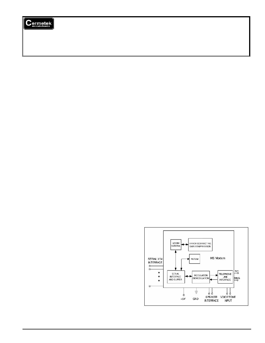
DESCRIPTION OF FUNCTIONAL BLOCKS
AND DISCUSSION OF BASIC OPERATIONS
Figure 1 contains a functional block drawing of the HS
Modem family of products. Each HS Modem product
consists of a serial interface buffer,
modulator/demodulator, modem controller with error
correction and data compression, non-volatile RAM
and a DAA.
Figure 1. Functional Block Diagram of HS Modem
Family.

Cermetek Microelectronics, Inc.
High Speed Modem and FAX Family
2003 Cermetek Microelectronics, Inc.
Page 2
Document No. 607-0003 Revision K1 (06/03)
Serial Host Interface Buffer. The HS Modem utilizes
a serial V.24 EIA 232-E 5V interface to control the
modem. The HS Modem products can communicate
over the serial interface with the Data Terminal
Equipment (DTE) at a fixed speed regardless of the
carrier line modulation speed (DCE) of the PSTN
modem connection. This eliminates the need to have
the DTE step up or step down in speed based on the
in-coming or out-going PSTN communication data
rate. Hence, the DTE can train the CH2056, to say
56kbps, and talk to a slower in-coming data
connection at say, 2400bps without changing host
speed. Conversely, the host DTE trained at 14.4kbps
can also communicate with the modems at higher
speeds, say 28.8kbps. This is accomplished by
invoking internal automatic data flow control. The HS
Modem family has a resident buffer to allow for this
auto baud operation.
Non-Volatile RAM (NVRAM). NVRAM can store
user-customized configurations. The AT&Wn
command will store the active modem configuration in
one of two NVRAM locations as selected by an n of 0
or 1. The AT&Yn command selects one of the stored
modem configurations to be automatically recalled and
made active upon reset or power up. The ATZn
command immediately recalls and activates a stored
configuration. See Tables 7A and 7B for storable S-
Registers and Commands.
The NVRAM can save up to four telephone numbers,
with up to 31 digits or modifiers in each telephone
number. The AT&Zn=s command will store s, the
telephone number dial string. The ATDS=n command
will cause the modem to dial one of the four stored
telephone numbers. The NVRAM storage location for
the four telephone numbers is selected by an n of 0, 1,
2, or 3.
Telephone Line Interface or DAA. High performance
modems are extremely sensitive to DAA (Data Access
Arrangement) performance. The difference between a
good modem and a fair one is in the DAA
performance. The HS Modem family includes a
unique low distortion DAA designed for optimal
performance over all PSTN line conditions thereby
achieving the most reliable and best performance
PSTN connections.
The HS Modem family is designed to meet North
American telephone standards as set by the FCC Part
68 (USA) and CSA CS-03 Part I (Canada). Among the
more critical parameters, the PSTN line interface is
designed to meet 1500 VAC RMS isolation and
provide 2122V peak surge protection. Consequently,
the HS Modem family of products satisfies U.S. and
Canadian requirements, and will meet other
international approval agency requirements that
specify these levels of isolation. The TBR/ETBR
variants also meet the European TBR21 requirements.
Pins 1 and 2 function as both input and output
connections to the PSTN. To maximize field reliability
in hostile environments, for Canadian approval, for UL
compliance, and also optionally for FCC Part 15
compliance, these two pins must be routed through an
external network such as that briefly described in
Figure 6A and described in more detail in Cermetek
Application Note # 126.
Each HS Modem product comes with FCC Part 68
approval and is shipped from the factory with an FCC
Label indicating registration number and ringer
equivalent. This label should be prominently displayed
on the end product. With the exception of the U.S.,
most countries (including Canada) require submission
of the final product or system containing the HS
Modem to the appropriate governing regulatory
agency for approval. Typically this is accomplished by
submitting the final end product to an independent test
house or consultant for evaluation. The test
house/consultant then forwards the test results and
applicable documents to the regulatory agency.
Contact Cermetek for a list of suggested consultants.
Modulation/Demodulation/Error Correcting and
Data Compression. These functions are provided by
an industry standard modem chip set which has been
adapted for use with the HS Modem family. The
Modulation/Demodulation scheme supports the
industry modem standards listed below.
SUPPORTED MODULATION STANDARDS
Bell 103
CCITT V.22
Bell212A
CCITT
V.22bis
CCITT
V.32
CCITT
V.32bis
CCITT
V.34
CCITT
V.34bis
CCITT
V.90
The HS Modem supports V.42 LAMP, MNP 2-4, MNP
10 error correcting protocols. The CH1794 uses
MNP5 data compression techniques and the
CH1799/CH2056 uses V.42bis data compression,
allowing data transmission rates of up to a maximum
of 57.6kbps/115.2kbps/230.4kbps, respectively.
These high DTE data rates are supported by the HS
Modem serial interface via its auto baud capability.
Note that the maximum speed attained is limited by
the maximum speed available from the DTE.
The resident Modulator/Demodulator supports line
equalization and forward error correction.
IMPORTANT NOTE
The V.90 standard prescribes 56kbps
downlink and 33.6kbps uplink. Consequently,
two V.90 modems connected back-to-back will
send at 33.6kbps.

Cermetek Microelectronics, Inc.
High Speed Modem and FAX Family
2003 Cermetek Microelectronics, Inc.
Page 3
Document No. 607-0003 Revision K1 (06/03)
CONNECTING TO THE HOST UART
Since a modem communicates data serially and most
host products handle data in a parallel format, a UART
is needed to make parallel-to-serial and serial-to-
parallel translations.
SUPPORTED FEATURES
AT Command Set. The HS Modem supports the AT
Command set with extensions and can operate with
industry standard communication software. The AT
Commands are compatible with TR302.2/88-08006.
Serial Host Interface. The HS Modem family
operates in asynchronous mode and supports a 5V,
RS232- like interface called V.24 (EIA-232-E). The HS
Modem supports a full RS-232C/V.24 serial interface.
Signal levels are TTL rather than RS-232C level
compatible, which allows direct connection of the HS
Modem to the host's UART without level translating
circuitry. See Table 3 for a complete set of pin
descriptions.
The modem is controlled by sending serial commands
over TXD and by monitoring serial status messages
returned on RXD. All other serial interface lines may
be utilized for the convenience of a particular
application but are not required by the modem.
Unused outputs from the HS Modem should be left
unconnected. Unused inputs should be tied to the
proper logic level. See Table 3.
Speaker Interface. The SPK output reflects the
receiver analog input and provides a signal that can be
used to monitor call progress. The SPK signal can
drive a 300-ohm load directly. Typically, the SPK
signal is input into an audio power amplifier and the
amplifier, in turn, drives the speaker coil. The speaker
is activated with the ATM command. The speaker
volume is adjusted using the ATLn command; where n
is 0, 1, 2, or 3. Increasing numbers correspond to
higher volume. Figure 3 indicates one method of
driving an external 8-ohm speaker.
Zero Power Mode. If an application calls for zero
power during standby periods, the power may be
switched off using external circuitry and then reapplied
when the HS Modem's RI pin becomes active. The
HS Modem can thus be powered down to zero.
Referring to Figure 2, the controller activates the relay
switch, supplying power (+5V) to the HS Modem. In
this configuration, the ring signal is used to "wake up"
the HS Modem when the HS Modem is in the power
down state.
The internal structure of the RI pin consists of an open
collector opto transistor with a 30k ohm pull-up through
a blocking diode to 5V. The user should apply his own
pull-up resistor to an active 5V source when the HS
Modem is powered down. The internal blocking diode
provides supply isolation.
The pins of the HS Modem will be in an undefined
state when powered is switched off. This must be
taken into consideration to assure that no unwanted
signals are presented to the HS Modem during power
down.
Figure 2. Zero Power Operation.
Power Supply. The HS Modem module is a complex
set of sensitive subsystems. During the course of
normal operation, the HS Modem decodes analog
signals from the telephone line that are in the millivolt
range. Steps must be taken by the user to guarantee
that power supply noise on all supply lines, including
ground, does not exceed 25mV peak to peak. If
necessary, use dedicated power and ground planes.
Failure to provide such operating conditions could
cause the HS Modem to malfunction or to function
erratically.
The HS Modem family requires +5V ±5% supply. It is
recommended that bypass capacitors be placed on the
power supply as close to the HS Modem's supply input
pins as practical. It is recommended that a 10 µF or
greater tantalum capacitor in parallel with a 0.1 µF
ceramic capacitor be used. The user must also
provide shielding from nearby sources of EMI, such as
relays, motors and other power supplies.
Automatic Speed/Format Sensing. The HS Modem
supports both Command and Data modes of
operation.
The HS Modem can automatically determine the
speed and format of the data sent from the DTE over
the serial interface; and can sense the following broad
range of speeds:

Cermetek Microelectronics, Inc.
High Speed Modem and FAX Family
2003 Cermetek Microelectronics, Inc.
Page 4
Document No. 607-0003 Revision K1 (06/03)
CH1794
300, 600, 1200, 2400, 4800, 7200,
9600, 12000, 14400, 19200, 38400, and
57600bps.
CH1799
300, 600, 1200, 2400, 4800, 7200,
9600, 12000, 14400, 16800, 19200,
21600, 24000, 26400, 28800, 38400,
57600, and 115200bps.
CH2056
300, 600, 1200, 2400, 4800, 7200,
9600, 12000, 14400, 16800, 19200,
21600, 24000, 26400, 28800, 38400,
57600, 115200, and 230400bps.
The data formats in Table 1 are recognized by the HS
Modem family of products.
Table 1. Data Formats Recognized by HS Modem
Family.
Parity
Data Length
(No. of Bits)
No. of
Stop
Bits
Character
Length
(No. of Bits)
None 7
2
10
Odd 7
1
10
Even 7
1
10
None 8
1
10
Odd 8
1 11*
Even 8
1
11*
*11 bit characters are sensed, but the parity bits are
stripped off during data transmission in Normal and
Error Correction modes.
The HS Modem can sense data with mark or space
parity and configures itself as described in Table 2.
The HS Modem is trained to a selected speed with an
AT<CR> training sequence. Thus, the DTE to modem
serial interface speed can be set independent of the
DCE or line carrier connecting speed (with minor
restrictions, see the AT+ MS command). This allows
greater flexibility when selecting DCE line carrier
modulation speed thereby affording the user with
optimum data throughput performance. To maximize
effective modem data throughput speed, the DTE to
modem serial interface speed should be set to the
highest speed available without invoking the use of the
HS Modem's built-in flow control. Although flow
control facilitates communication with higher speed
modes by the DTE, use of flow control causes an
overall throughput data rate penalty.
Voice/Tone Injection Port. The HS Modem Family
provides pin T1 to allow the user to share the PSTN
line interface associated with the modem for voice and
DTMF applications. Figure 5 contains a schematic
which uses a 5 Volt single supply operational amplifier
and indicates one possible configuration for voice/tone
utilization.
Refer to Cermetek Application Note #170, 2-4 Wire
Converter for Use with CH179X and CH2056 Modems,
for an alternative voice/tone implementation that
utilizes dual supply operational amplifiers.
Table 2. HS Modem Auto Configuration Based on
DTE Configuration.
DTE Configuration
HS Modem
Configuration
7 mark
7 none
7 space
8 none
8 mark
8 none
8 space
8 even
Figure 3. Speaker Control Circuit.
All HS Modem products are designed with pin T1
coupled directly to the internal DAA. When using the
HS Modem in data mode, T1 should float and be
disconnected from any potential signal because any
signal on T1 during data operation will affect the HS
Modem's output. If T1 is being asserted from another
application, use a relay or zero impedance switch to
disconnect T1 when in data mode.
When voice and data are both being used, and the T1
pin is active, it is typical for voice communication to
precede data communication. In this case, the
following commands should be used to configure the
HS Modem to allow for full utilization of the Voice/Tone
injection feature. These commands disable auto-
answer and eliminate hang-up due to lack of carrier
signal.
1. Enter:
ATS0=0<CR>
2. Enter:
ATS7=255<CR>
3. Enter:
ATS10=255<CR>
The following command sequences illustrate
implementation of common voice/tone port
applications.
1. To answer a voice call:
(a) Enter: ATH1<CR>
(b) Switch local voice source into T1
(c) Begin Voice Conversation
Cermetek Microelectronics, Inc.
High Speed Modem and FAX Family
2003 Cermetek Microelectronics, Inc.
Page 5
Document No. 607-0003 Revision K1 (06/03)
2. To switch to data mode, switch local voice source
from T1:
(a) At the Originate Modem, enter: ATX1<CR>
(b) At the Answer Modem, enter: ATA<CR>
3. To disconnect (hang-up) a voice call or data call:
(a) Return to control mode by entering: +++
(b) Enter: ATH<CR>
4. To place a voice call using the HS Modem DTMF
facilities:
(a) Enter: ATDT1234567<CR>
Where 1234567 is the phone number
(b) Then switch to local voice source
MODEM CONTROL
The HS Modem may be controlled by sending serial
ASCII command sequences. The commands are sent
to the modem serially on the TXD pin. After execution
of a received command, the modem returns a serial
status message that completion status. Refer to Table
5A, 5B and 5C for a complete list of status messages.
MODEM STATES
The HS Modem can be in either command mode or
data mode. When the modem is idle, it is in command
mode by default and will recognize commands. When
data transmission is in progress, the HS modem is in
the data mode state and will not recognize commands.
To force the HS Modem to recognize commands, the
host must send an "escape sequence" to the HS
Modem forcing it out of data mode and into command
mode.
The escape sequence consists of a "guard time" (a
period where no characters are sent to the modem),
followed by 3 escape characters, followed by a second
guard time. At power-up, the guard time is set to 1
second, and the escape character is set as "+." Note
that a 50 msec delay is required between escape
characters. These two parameters can be modified
via registers S2 and S12, respectively.
The HS modem will stay off-hook with its carrier on
after the escape sequence is received. The HS
Modem will return an OK status message when it is
ready to accept commands. To put the HS Modem
back into data mode, issue command ATO<CR>.
THE COMMAND FORMAT
HS Modem commands consist of three elements:
1. The
attention
sequence,
2. The commands themselves and
3. A terminating carriage return.
Enter:
ATDT1234567<CR>
Result: Modem goes off-hook and tone dials phone
number 1234567.
WARNING
The HS Modem family of products has been FCC
Part 68 approved as data/FAX modems. Utilization
of the Voice/Tone Port requires further registration.
The FCC requires that the entire system, including
the HS Modem and the handset or DTMF
transceiver, adhere to Part 68 rules.
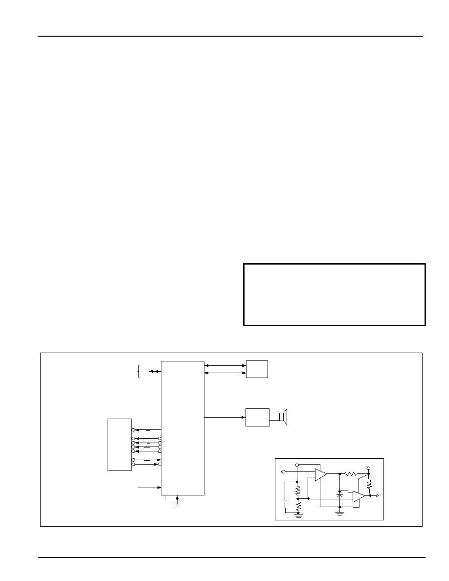
Figure 4. HS Modem Family Application Diagram.
RXD
DCD
DSR
RI
CTS
TXD
DTR
+5V
GND
V.24
EIA-232-E
INTERFACE
OR
UART
TIP
RING
RJ-11
JACK
SPK
SPEAKER
CONTROL
NOTE: SPEAKER CONTROL AND PHONE
CONTROL ARE ANCILLARY CIRCUITS
SHOWN ELSEWHERE IN THIS DATA SHEET.
HS MODEM
FAMILY
ANALOG VOICE
INJECTED SIGNALS
T1
EXTERNAL RESET
RST
*
SIGNAL GND MUST BE CONNECTED TO
EARTH GROUND
Vcc
Isolated
Envelope
Ring Detect
4.7uF
Vcc
10K
4.7K
22K
10K
.1uF
+
-
-
+
LM393
LM393
1
2
3
4
5
6
7
8
RI