 | –≠–ª–µ–∫—Ç—Ä–æ–Ω–Ω—ã–π –∫–æ–º–ø–æ–Ω–µ–Ω—Ç: CS209AYD8 | –°–∫–∞—á–∞—Ç—å:  PDF PDF  ZIP ZIP |
1
Features
OSC
Feedback
GND
V
CC
23.6k
W
4.8k
W
300
mA
V
CC
OSC
RF
TANK
DEMOD
OUT
1
OUT
2
Neg Transient
Suppression
Oscillator
DEMOD
VBE/R Current
Regulator
COMP
+
-
DVBE/R Current
Regulator
s
Separate Current
Regulator for Oscillator
s
Negative Transient
Suppression
s
Variable Low-Level
Feedback
s
Improved Performance
over Temperature
s
6mA Supply Current
Consumption at
V
CC
= 12V
s
Output Current Sink
Capability
20mA at 4V
CC
100mA at 24V
CC
Package Options
8L PDIP & SO
14L SO
CS209A
Proximity Detector
7
8
1
2
3
4
5
6
OSC
TANK
Gnd
OUT
1
RF
V
CC
DEMOD
OUT
2
10
7
14
13
12
8
1
2
3
4
5
6
11
9
OSC
TANK
Gnd
OUT
1
N.C.
OUT
2
N.C.
N.C.
RF
V
CC
N.C.
DEMOD
N.C.
N.C.
CS209A
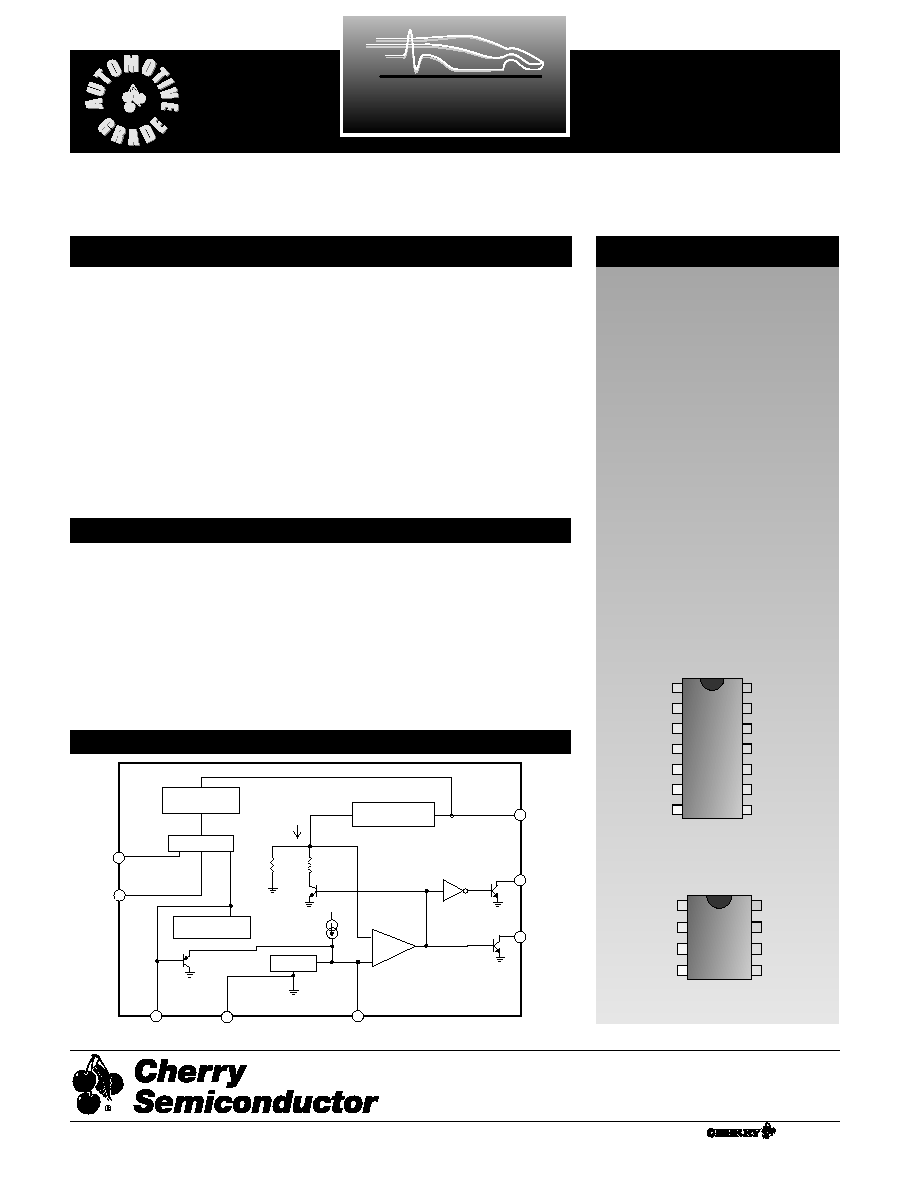
Description
The CS209A is a bipolar monolithic
integrated circuit for use in metal detec-
tion/proximity sensing applications.
The IC (see block diagram) contains two
on-chip current regulators, oscillator
and low-level feedback circuitry, peak
detection/demodulation circuit, a com-
parator and two complementary output
stages.
The oscillator, along with an external
LC network, provides controlled oscilla-
tions where amplitude is highly depen-
dent on the Q of the LC tank. During
low Q conditions, a variable low-level
feedback circuit provides drive to main-
tain oscillation. The peak demodulator
senses the negative portion of the oscil-
lator envelop and provides a demodu-
lated waveform as input to the com-
parator. The comparator sets the states
of the complementary outputs by com-
paring the input from the demodulator
to an internal reference. External loads
are required for the output pins.
A transient suppression circuit is
included to absorb negative transients
at the tank circuit terminal.
Block Diagram
Absolute Maximum Ratings
Supply Voltage ................................................................................................24V
Power Dissipation (T
A
= 125°C).............................................................200mW
Storage Temperature Range ....................................................–55°C to +165°C
Junction Temperature...............................................................–40°C to +150°C
Electrostatic Discharge (except TANK pin) ................................................2kV
Lead Temperature Soldering
Wave Solder(through hole styles only) ...........10 sec. max, 260°C peak
Reflow (SMD styles only) ...........60 sec. max above 183°C, 230°C peak
A Company
®
Rev. 3/11/99
Cherry Semiconductor Corporation
2000 South County Trail, East Greenwich, RI 02818
Tel: (401)885-3600 Fax: (401)885-5786
Email: info@cherry-semi.com
Web Site: www.cherry-semi.com

2
Electrical Characteristics: -40°C ≤ T
A
≤ 125°C unless otherwise specified
PARAMETER
TEST CONDITIONS
MIN
TYP
MAX
UNIT
CS209A
8
6
4
2
100
4
8
12
16
20
Switching Delay (
m
s)
Output Load (k
W)
(T = 22
∞C, V
CC
= 12V)
-40
-20
0
20
40
60
80
100
120
2.5
3.5
4.5
5.5
6.5
Switching Delay (
m
s)
Temperature (
∞C)
(V
CC
= 12V, R
load
= 1k
W)
Output Switching Delay vs. Temperature
Output Switching Delay vs. Output Load
Typical Performance Characteristics
Package Pin Description
PACKAGE PIN#
PIN SYMBOL
FUNCTION
8L PDIP & SO
14L SO
1
1
OSC
Adjustable feedback resistor connected between OSC and
RF sets detection range.
2
2
TANK
Connects to parallel tank circuit.
3
3
Gnd
Ground connection.
4
4
OUT
1
Complementary open collector output; When OUT
1
=
LOW, metal is present.
5
6
OUT
2
Complementary open collector output; When OUT
2
=
HIGH, metal is present.
6
10
DEMOD
Input to comparator controlling OUT
1
and OUT
2
.
7
12
V
CC
Supply voltage.
8
13
RF
Adjustable feedback resistor connected between OSC and
RF set detection range.
5,7,8,9,11,14
NC
No Connection.
Supply Current I
CC
V
CC
= 4V
3.5
6.0
mA
V
CC
= 12V
6.0
11.6
mA
V
CC
= 24V
11.0
20.0
mA
Tank Current
V
CC
= 20V
-550
-300
-100
µA
Demodulator Charge Current V
CC
= 20V
-60
-30
-10
µA
Output Leakage Current
V
CC
= 24V
0.01
10.00
µA
Output V
SAT
V
CC
= 4V, IS =20mA
60
200
mV
V
CC
= 24V, IS =100mA
200
500
mv
Oscillator Bias
V
CC
= 20V
1.1
1.9
2.5
V
Feedback Bias
V
CC
= 20V
1.1
1.9
2.5
V
Osc - Rf Bias
V
CC
= 20V
-250
100
550
mV
Protect Voltage
I
TANK
= -10mA
-10.0
-8.9
-7.0
V
Detect Threshold
720
1440
1950
mV
Release Threshold
550
1200
1700
mV
3
0.400
0.300
0.200
0.100
0.0
0.75
1.0
1.25
1.5
1.75
DEMOD (V)
Distance To Object (in.)
2.5k
W
5k
W 7.5kW
12.5k
W
15k
W
17.5k
W
Object
Detected
Object Not
Detected,
L Unloaded.
(T = 21
∞C, V
CC
= 12V)
Demodulator Voltage vs. Distance for Different RF
Typical Performance Characteristics: continued
The CS209A is a metal detector circuit which operates on
the principle of detecting a reduction in Q of an inductor
when it is brought into close proximity of metal. The
CS209A contains an oscillator set up by an external parallel
resonant tank and a feedback resistor connected between
OSC and RF. (See Test and Applications Diagram) The
impedance of a parallel resonant tank is highest when the
frequency of the source driving it is equal to the tank’s res-
onant frequency. In the CS209A the internal oscillator
operates close to the resonant frequency of the tank circuit
selected. As a metal object is brought close to the inductor,
the amplitude of the voltage across the tank gradually
begins to drop. When the envelope of the oscillation reach-
es a certain level, the IC causes the output stages to switch
states.
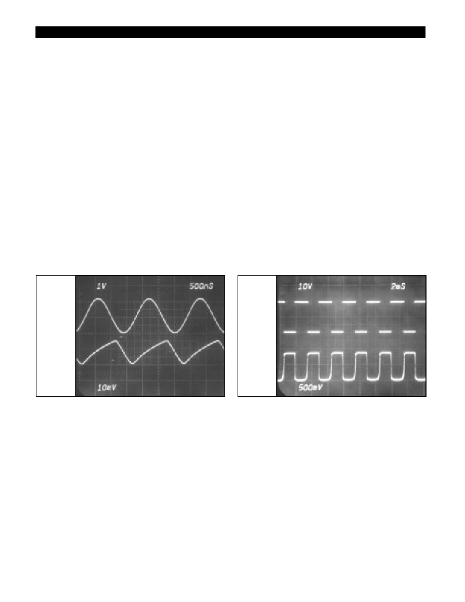
The detection is performed as follows: A capacitor con-
nected to DEMOD is charged via an internal 30µA current
source. This current, however, is diverted away from the
capacitor in proportion to the negative bias generated by
the tank at TANK. Charge is therefore removed from the
capacitor tied to DEMOD on every negative half cycle of
the resonant voltage. (See Figure 1) The voltage on the
capacitor at DEMOD, a DC voltage with ripple, is then
directly compared to an internal 1.44V reference. When the
internal comparator trips it turns on a transistor which
places a 23.6kΩ resistor in parallel to the 4.8kΩ. The result-
ing reference then becomes approximately 1.2V. This hys-
teresis is necessary for preventing false triggering.
The feedback potentiometer connected between OSC and
RF is adjusted to achieve a certain detection distance
range. The larger the resistance the greater the trip-point
distance (See graph Demodulator Voltage vs Distance for
Different RF). Note that this is a plot representative of one
particular set-up since detection distance is dependent on
the Q of the tank. Note also from the graph that the capaci-
tor voltage corresponding to the greatest detection dis-
tance has a higher residual voltage when the metal object
Principle of Operation
is well outside the trip point. Higher values of feedback
resistance for the same inductor Q will therefore eventu-
ally result in a latched-ON condition because the residual
voltage will be higher than the comparator’s thresholds.
As an example of how to set the detection range, place the
metal object at the maximum distance from the inductor
the circuit is required to detect, assuming of course the Q
of the tank is high enough to allow the object to be within
the IC’s detection range. Then adjust the potentiometer to
obtain a lower resistance while observing one of the
CS209A outputs return to its normal state (see Test and
Applications Diagram). Readjust the potentiometer slow-
ly toward a higher resistance until the outputs have
switched to their tripped condition. Remove the metal
and confirm that the outputs switch back to their normal
state. Typically the maximum distance range the circuit is
capable of detecting is around 0.3 inch. The higher the Q,
the higher the detection distance.
For this application it is recommended to use a core
which concentrates the magnetic field in only one direc-
tion. This is accomplished very well with a pot core half.
The next step is to select a core material with low loss fac-
tor (inverse of Q). The loss factor can be represented by a
resistance in series with the inductor which arises from
core losses and is a function of frequency.
The final step in obtaining a high Q inductor is the selec-
tion of wire size. The higher the frequency the faster the
decrease in current density towards the center of the wire.
Thus most of the current flow is concentrated on the sur-
face of the wire resulting in a high AC resistance. LITZ
wire is recommended for this application. Considering
the many factors involved, it is also recommended to
operate at a resonant frequency between 200 and 700kHz.
The formula commonly used to determine the Q for par-
allel resonant circuits is:
Q
P
@
R
2πf
R
L
CS209A
4
where R is the effective resistance of the tank. The resis-
tance component of the inductor consists primarily of core
losses and “skin effect” or AC resistance.
The resonant capacitor should be selected to resonate with
the inductor within the frequency range recommended in
order to yield the highest Q. The capacitor type should be
selected to have low ESR: multilayer ceramic for example.
Detection distances vary for different metals. Following
are different detection distances for some selected metals
and metal objects relative to one particular circuit set-up:
Commonly encountered metals:
• Stainless steel
0.101"
• Carbon steel
0.125"
• Copper
0.044"
• Aluminum
0.053"
• Brass
0.052"
Coins:
• US Quarter
0.055"
• Canadian Quarter
0.113"
• 1 German Mark
0.090"
• 1 Pound Sterling
0.080"
• 100 Japanese Yen
0.093"
• 100 Italian Lira
0.133"
12 oz. soda can:
0.087"
Principle of Operation: continued
Note that the above is only a comparison among different
metals and no attempt was made to achieve the greatest
detection distance.
A different type of application involves, for example,
detecting the teeth of a rotating gear. For these applica-
tions the capacitor on DEMOD should not be selected too
small (not below 1000pF) where the ripple becomes too
large and not too large (not greater than 0.01µF) that the
response time is too slow. Figure 1 for example shows the
capacitor ripple only and Figure 2 shows the entire capaci-
tor voltage and the output pulses for an 8-tooth gear rotat-
ing at about 2400 rpm using a 2200pF capacitor on the
DEMOD pin.
Because the output stages go into hard saturation, a time
interval is required to remove the stored base charge
resulting in both outputs being low for approximately 3µs
(see Output Switching Delay vs. Temperature graph). If
more information is required about output switching
characteristics please consult the factory.
Figure 1. Capacitor ripple.
Figure 2. Output pulse for an 8 tooth gear.
CS209A
V
OUT
1
V
DEMOD
V
TANK
V
DEMOD

5
CS209A
Test and Application Diagram
20k
W
4300pF
Gnd
V
CC
RL
1k
W
RL
1k
W
NORMALLY
HI
NORMALLY
LO
CDEMOD
2200 pF
L
OSC
RF
TANK
DEMOD
OUT
1
OUT
2
L: Core: Siemens B65531-D-R-33
52 Turns, 6x44 AWG, Litz Unserved
Single Polyurethane
CS209A
6
CS209A
Rev. 3/11/99
Part Number
Description
CS209AYN8
8 L PDIP
CS209AYD8
8L SO Narrow
CS209AYDR8
8L SO Narrow (tape & reel)
CS209AYD14
14L SO Narrow
CS209AYDR14
14L SO Narrow (tape & reel)
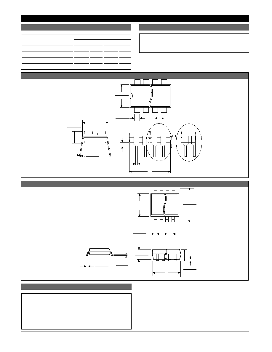
Ordering Information
Thermal Data
8L PDIP
8L SO
14L SO
R
QJC
typ
52
45
30
°C/W
R
QJA
typ
100
165
125
°C/W
D
Lead Count
Metric
English
Max
Min
Max
Min
8L PDIP
10.16
9.02
.400
.355
8L SO
5.00
4.80
.197
.189
14L SO
8.75
8.55
.344
.337
Package Specification
PACKAGE DIMENSIONS IN mm (INCHES)
PACKAGE THERMAL DATA
© 1999 Cherry Semiconductor Corporation
Cherry Semiconductor Corporation reserves the
right to make changes to the specifications without
notice. Please contact Cherry Semiconductor
Corporation for the latest available information.
Plastic DIP (N); 300 mil wide
0.39 (.015)
MIN.
2.54 (.100) BSC
1.77 (.070)
1.14 (.045)
D
Some 8 and 16 lead
packages may have
1/2 lead at the end
of the package.
All specs are the same.
.203 (.008)
.356 (.014)
REF: JEDEC MS-001
3.68 (.145)
2.92 (.115)
8.26 (.325)
7.62 (.300)
7.11 (.280)
6.10 (.240)
.356 (.014)
.558 (.022)
Surface Mount Narrow Body (D); 150 mil wide
1.27 (.050) BSC
0.51 (.020)
0.33 (.013)
6.20 (.244)
5.80 (.228)
4.00 (.157)
3.80 (.150)
1.57 (.062)
1.37 (.054)
D
0.25 (0.10)
0.10 (.004)
1.75 (.069) MAX
1.27 (.050)
0.40 (.016)
REF: JEDEC MS-012
0.25 (.010)
0.19 (.008)