Features
Line 1
Controller
Line N
S-ART
s
Receives/Transmits Data
on Only Two Leads
s
Low Current Consumption
s
High Noise Immunity
s
Sabotage Surveilled Loop
Input
Package Options
CS212
Security Detector
Serial-Addressable Receiver/Transmitter
CS212
Description
The S-ART is a 16 pin circuit
designed for data transmission on a
two-lead cable. The circuit is spe-
cially developed for alarm systems
where it is desired to identify each
detector individually. There can be
up to 30 S-ART circuits/detectors
on the same 2-lead cable. This cable
transmits both DC supply to the
S-ART and information to/from the
S-ART.
The S-ART works on the principle
by which an address is sent on the
line cable and the S-ART which rec-
ognizes the address then carries out
the order which can, in principle, be
two things:
1. Transmit data from the line cable
to the S-ART's two outputs OUT0
and OUT1.
2. Answer the S-ART controller
with the condition of the 2 inputs
IN0 and IN1 or IN2-3.
The line signal is divided into 3 lev-
els in order to give a time signal for
synchronizing and a data signal
containing addresses, orders etc.
Typical signal levels for the three
levels would be 15V, 7.5V and 0V.
Block Diagram
1
OUT0
2
3
4
5
6
7
8
A4
A3
A2
A1
A0
IN1
IN0
16
15
14
13
12
11
10
9
OUT1
DSR
IN2
IN3
V
DD
DATA
OUT
Gnd
LINE
16L PDIP & 16L SO Wide
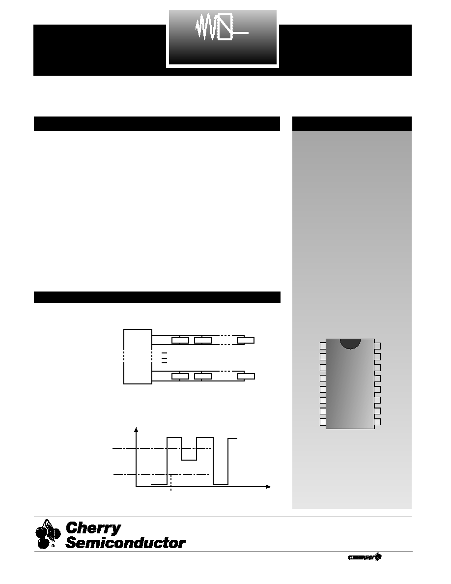
1
A method by
which, in principle,
the system can be
extended to an
infinite number of
S-ART is shown on
the block diagram.
The controller
scans the in/out-
puts of a number
of lines, each with
a maximum of 30
S-ARTs.
CK "1"
V
DATA "1"
DATA "0"
Cherry Semiconductor Corporation
2000 South County Trail, East Greenwich, RI 02818
Tel: (401)885-3600 Fax: (401)885-5786
Email: info@cherry-semi.com
Web Site: www.cherry-semi.com
A Company
�
Rev. 4/21/99

Lead Temperature Soldering:
Wave Solder (through hole styles only) . . . . . . . . . . . . . . . . . . . . . . . . . . . . . . . . . . . . . . . . . . . .10 Sec. max 260�C Peak
Reflow (SMD styles only) . . . . . . . . . . . . . . . . . . . . . . . . . . . . . . . . . . . . . . . . . . . .60 Sec max. above 183�C, 230�C Peak
Storage Temperature Range, T
S
. . . . . . . . . . . . . . . . . . . . . . . . . . . . . . . . . . . . . . . . . . . . . . . . . . . . . . . . . . . . . . . .-65 to 150�C
Maximum Operating Junction Temperature, T
J
. . . . . . . . . . . . . . . . . . . . . . . . . . . . . . . . . . . . . . . . . . . . . . . . . . . . . . . .125�C
Electrical Characteristics: T
A
= 25�C, unless otherwise specified.
PARAMETER
TEST CONDITIONS
MIN
TYP
MAX
UNIT
CS212
2
Absolute Maximum Ratings
Operating Temperature Range, T
A
-40
85
�C
Device Current I
DD
Outputs unloaded
0.47
0.80
mA
Not Addressed
Line Voltage=0-15V, V
DD
=15V
Device Current I
DD
IN0, IN1 are Open
3.55
5.50
mA
Power-Up-Mode
IN2, IN3 are Active
(5 corr. addr. bits)C
P
4-C
P
5
V
DD
=15V
Device Current I
DD
IN2, IN3 not Active
6.24
9.64
mA
Addressed, Line Output
IN0, IN1 are Open
Transistor Active
V
DD
=15V
Device Current I
DD
IN2, IN3 not Active
1.84
2.86
mA
Addressed (4 corr.addr.bits)
IN0, IN1 are Open
Line Output Transistor Not Active
V
DD
=15V
Output Voltage Low Level
V
DD
=10-15V
1.2
V
Out0, Out1, DSR
I
SINK
=1mA
Output sink Current
1.0
mA
Out0, Out1, DSR
Output Voltage High Level
14
V
Out0, Out1, DSR
Leakage Current
V
OUT
=14V
30
�A
Out0, Out1, DSR
Input Voltage Level
Low
V
DD
=10-15V
30%V
DD
V
A0-A4, IN0, IN1 High
V
DD
=10-15V
70%V
DD
V
Input Current IN0, IN1=Gnd
V
DD
=18V
150
850
�A
Power-Up Mode
(4 corr.addr.bits)
Input Current
V
DD
=18V
20
�A
A0-A4, IN0, IN1
Not Addressed
Positive Trigger
Threshold V
P
, C
Clock Comparator
11.0
11.7
12.4
V
Voltage V
dd
=15V V
P
, D
Data Comparator
4.6
5.7
6.6
V
Negative Trigger V
NC
V
DD
=15V Clock Comparator
10.2
10.9
11.6
V
Threshold Voltage V
NC
V
DD
=15V, Data Comparator
3.4
4.3
5.2
V
Hysteresis Voltage
V
DD
=15V
0.7
0.8
V
Clock/Data Comp.
Saturation Voltage For
V
DD
=15V, I
C
=50mA
1
V
Line Output Driver
Saturation Voltage For
V
DD
=15V, I
C
=10mA
0.4
V
Line Output Driver
Leakage Current
V
LINE
=0-18V, V
DD
=18V
�16
�A
For the Line Output
Line Signal Freq.
V
DD
=15V�1V
0
20
kHz
Rise/Fall-Time Line Signal
0.25
250.00
�s

PARAMETER
TEST CONDITIONS
MIN
TYP
MAX
UNIT
CS212
3
Electrical Characteristics: T
A
= 25�C, unless otherwise specified.
Package Pin Description
PACKAGE PIN #
PIN SYMBOL
FUNCTION
1
OUT0
Output (open collector) from S-ART.
2
A4
Address input. Must be connected to V
DD
or Gnd according to the
relevant address code.
3
A3
Address input. Must be connected to V
DD
or Gnd according to the
relevant address code.
4
A2
Address input. Must be connected to V
DD
or Gnd according to the
relevant address code.
5
A1
Address input. Must be connected to V
DD
or Gnd according to the
relevant address code.
6
A0
Address input. Must be connected to V
DD
or Gnd according to the
relevant address code.
7
IN1
Input to S-ART.
8
IN0
Input to S-ART.
9
LINE
Signal lead in the line cable.
10
Gnd
Zero lead in the line cable.
11
DATA
OUT
Output from the S-ART, which is active in the READ-mode.
Transmits data from
S-ART to line.
12
V
DD
Supply voltage to the S-ART. The voltage is derived from the line
signal.
13
IN3
Sabotage surveilled loop (shorting and breaking).
14
IN2
Sabotage surveilled loop (shorting and breaking).
15
DSR
Data Set Ready. Output (open collector) from the S-ART which is
active during WRITE-mode, when OUT0 and OUT1 change.
16
OUT1
Output (open collector) from S-ART.
Turn-On Time For
1.0
�s
Line Output Driver
Turn-Off Time For
1.0
�s
Line Output Driver
Line Voltage VL (Note 1)
0
28
V
Loop Current IN2, IN3
0.1
0.5
mA
Alarm Condition IN2-IN3
1
5
k�
Loop Open
Alarm Condition IN2-IN3
5
30
k�
Loop Shorted
Note 1: The circuit shall function in the correct way only between 0 and 18V
DC
. Data driver must not turn on when line voltage is above 18V.
4
CS212
Serial-Addressable Receiver Transmitter S-ART
ADDRESS CODING
The circuit is coded on address inputs A0-A4.
In order to reduce the power consumption to the circuits
they are in power down mode for most of the time. Only
when a circuit is addressed is the amount to that particular
circuit increased.
READ
When a S-ART has recognized an address with the correct
parity and then received a READ-order the controller
becomes passive. The S-ART in question will then send
data bits to the controller. These bits are the condition on
the IN0 and IN1 or IN2-3 and a parity bit derived from
them.
The current in inputs IN0 and IN1 only flows when the
S-ART is addressed.
If the sabotage surveilled loop IN2-3 is used IN1 should be
open. IN2-3 is then read instead of IN1.
The loop IN2-3 is checked for both shorting and breaking.
WRITE
When a S-ART has recognized an address with correct par-
ity and a write order, the S-ART in question transmits data
to the outputs OUT0 and OUT1. This data transmission
takes place after a check of the parity bit. If the parity bit is
wrong, data transmission to OUT0 and OUT1 is blocked
and new data transmission can only take place after a read
order which resets the parity fault.
The DSR signal can be used to strobe OUT0 and OUT1 fur-
ther on in the following logic.
DATA FORMAT
The signals are sent out on the line in words organized as
shown in the figure.
The S-ART information consists of two parity bits: an
address parity bit and a data parity bit. Both the address
and data are checked for even parity. The address parity
bit must always be generated by the controller. The data
parity bit during the READ-mode is generated by the
S-ART. During the WRITE-mode the data parity bit is gen-
erated by the controller.
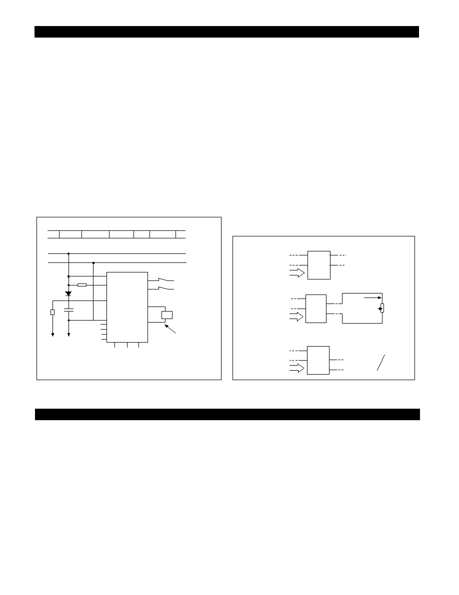
Typical S-ART Applications
S-ART
S-ART
1) Alarm Detector
Line from Controller
Address Coding
3) Alarm Indicator/Data Transmission
Line from Controller
Address Coding
IN0
IN1
Tamper Contact
Alarm Contact
Detector
Bells
Lamps etc.
Logic
Circuit
S-ART
2) Window Foil
Line from Controller
Address Coding
IN2
IN3
Foil
Terminal Lead
The foil is checked both for shorts and breakage.
Short Cables
End of Loop
Circuit
Address
Code
Transmission Line
Line
Data
Out
V
DD
Gnd
IN0
+
IN1
+
IN2
+
IN3
C
R1
A0
A4
OUT0 OUT1 DSR
Gnd
Gnd
R2
Addresses ADD. Parity
Command
Data
Data Parity
+
Indicates IN1 and Loop IN2, IN3 cannot be used at the same time.
Functional Description
GENERAL
The CS212 is a peripheral addressable circuit which is used
as a communication link between Detectors/Sensors and a
Central Control Unit.
The communication between the CS212 and a control unit
takes place via a simple 2-wire cable which also provides
power to the IC.
On each 2-wire cable, a maximum of 30 CS212's can be con-
trolled or interrogated with the address binary 0-29. This
permits surveillance of up to 30 window protections, door
contacts, movement detectors, etc. within the same 2-wire
group. Each CS212 can monitor the status of two external
surveillance devices and communicate the status back to
the control unit. Two outputs are also available for control-
ling bells, lights, LED's, door locks, etc. These outputs are
controlled from the control unit via the 2-wire cable.
WIRE TRANSMISSION CABLE (The Line)
The 2-wire bidirectional transmission cable called "The
Line" provides power and data to the CS212 and also pro-
vides data back to the control circuit.
The line signal is rectified and filtered at each CS212 and is
used for the power supply to the chip. The CS212 also
decodes the line signal into clock and data signals used
inside the IC.
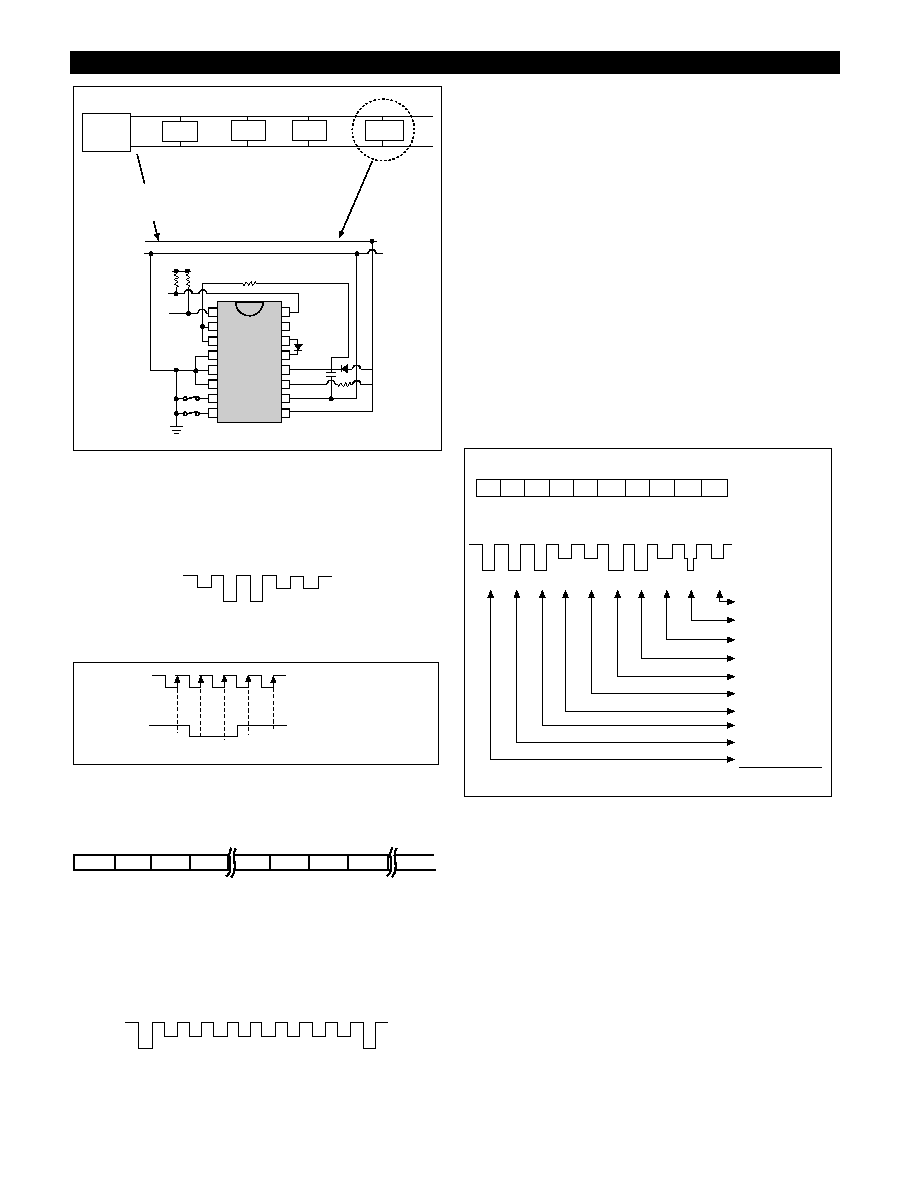
CS
5
CS212
Functional Description
Notes:
1. * Indicates IN1 & loop IN2-3 cannot be used at the same time.
2. This diagram shown CS212 circuit coded to #24.
A typical line signal from the control unit would look like
the following:
The CS212 would decode this into clock and data.
The CS212 accepts addresses and commands in 10-bit word
formats. Three types of words must be generated: Sync,
Read and Write.
SYNC WORD
Synchronization is obtained by providing the CS212 with 8
or more 1's followed by a "0". To prevent a false sync, it is
best to send 0 before the eight 1's. This word insures all cir-
cuits on the same line see the commands at the proper
time.
READ WORD
To check the status of a CS212's inputs: i.e., IN0 and IN1 or
IN2-3, a read word must be sent. The first 5 bits must cor-
respond to the address of the CS212 to be interrogated. Bit
#6 is the address parity bit. It must insure that the first 6
bits are an even number of "1" 's. If the parity is even and
the CS212 to be interrogated has not previously received a
parity error (odd parity), it will transmit its status, along
with an internally generated parity bit. D0 corresponds to
IN0, D1 corresponds to IN1 or IN2-3. After the address
parity bit has been transmitted the controller must pull the
line down to about 7.5V to allow the CS212 to transmit. If a
"1" is to be transmitted, no change will occur on the line. If
a "0" is to be transmitted, the CS212 will then pull the line
down. In either case, the controller must pull the line back
up to 15V in order to continue. If the CS212 has received a
parity fault, it will transmit 3 one's (D0=D1=P
D
=1). This
will allow the controller to detect a parity error. If a parity
error is detected by the controller, the read word must be
repeated.
TYPICAL READ WORD
Assume that device #24 is to be interrogated and the status
of IN0=1 and IN1=0.
WRITE WORD
In order to update OUT0 and OUT1, a write word must be
sent to the CS212. The first 5 bits must correspond to the
CS212 to be updated. Bit #6 is an address parity bit. It must
insure even parity. D0 corresponds to OUT0 and D1 corre-
sponds to OUT1. An even data parity bit must be received
by the CS212. If the address and data parity are even and
the CS212 has not previously received a parity error, it will
update OUT0 and OUT1. If a parity error was received, the
CS212 will not be updated. In this case, a read word must
be sent to clear the parity fault.
0
1
1
1
1
0
0
0
0
0
Data Parity
IN 1 Status
IN 0 Status
"0" for Read
Add Parity
A4=1 x 2
4
= 16
A3=1 x 2
3
= 8
A2=0 x 2
2
= 0
A1=0 x 21 = 0
A0=0 x 2
0
= 0
Binary = #24
0
1
1
1
1
0
0
0
0
0
A0 A1 A2 A3 A4 PA
READ
BIT
D0 D1
PD
Transmitted
by Controller
Transmitted
by CS-212
1
1
1
0
0
1
1
1
1
1
SYNC
READ
1
READ
2
READ
3
READ
29
SYNC WRITE
1
WRITE
2
WRITE
29
1
1
1
0
0
Clock
Data
Positive Edge Strobes
Data into an Internal
Shift Resister
1
1
1
0
0
1
2
3
4
5
6
7
8
16
15
14
13
12
11
10
9
Control
Circuit
2121
21229
2123
2122
2 Wire
Transmission
Line
V
CC
(<14V)
To Control
Bell/Det.
Etc.
10k
DET
Loop
1
mF
150
NC
N0
Tranmission Line