Features
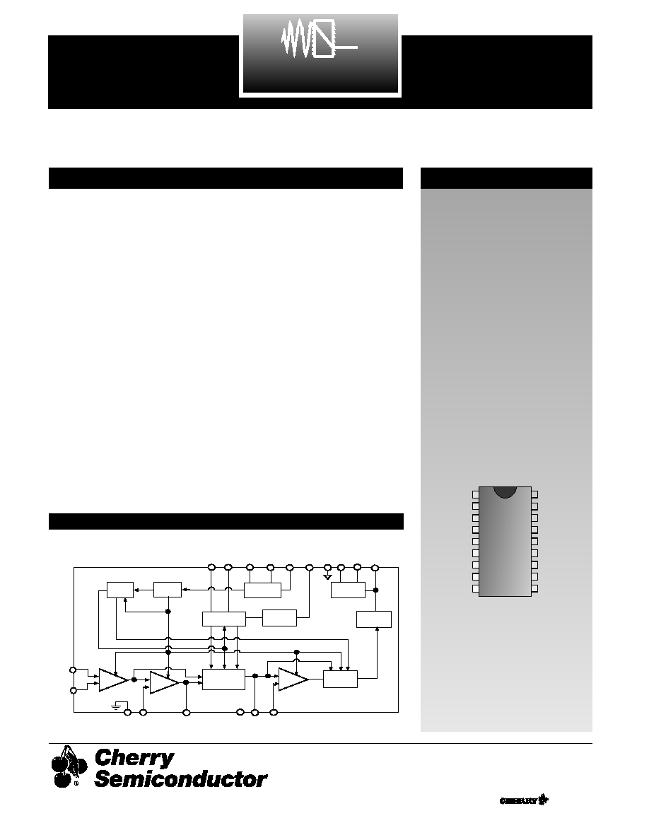
GATE
POWER
UP
GATE BIAS
SET
MAIN
TIMER
LED
DRIVER
OSCILLATOR
CURRENT
LIMITER
OUTPUT
LATCH
COUNTER
–3
•
•
CLOCK
POWER UP BIAS
COMP
SYNC
DETECTOR
A2
A1
DET
REF
DET
OUT
NC
A2
OUT
A2
IN
L.L.
GND
A1 IN
(+)
A1 IN
(-)
INT
BIAS
OSC
PGM
TIMER
CAP
PGM
RES
PULSE
WIDTH
LED H.L.
Gnd
V
R
I
CC
PGM
V
CC
/
OUT
s
Synchronous Detection
for High Noise Immunity
s
Pulsed Operation for Low
Average Current Drain
s
System Gain Externally
Set
s
System Sensitivity
Externally Adjustable
s
System Operation
Monitored by Means of
External Red LED
Package Options
CS235
System Photoelectric Smoke Detector
CS235
Description
The CS235 System Smoke Detector
is a photo electric type with a
pulsed infrared LED as the light
source and a silicon photodiode as
the light detector. The CS235 IC,
along with passive external compo-
nents, controls the system timing
and signal processing.
Low average current is attained by
pulsing the system once every 10
seconds for 20 milliseconds. Bias is
applied to the signal processing cir-
cuitry for this time interval. During
the second half of the pulse, the last
10 milliseconds, the IR LED is
pulsed and the unit samples for an
alarm level smoke condition. After
the first alarm level signal the sam-
ple rate increases to a two second
interval. After three consecutive
alarm level samples the logic drives
the output latch signalling the sys-
tem panel.
The signal processing circuit blocks
are amplifiers A1 and A2, syn-
chronous detector, voltage com-
parator and the decode counter.
The voltage gain of A2 and the
comparator reference voltage are
set by external resistors.
Additional on-chip features include
an I
CC
current limiter. The current
limiter eliminates power-on false
alarming.
The oscillator controls the IR LED
excitation frequency and provides
drive to the synchronous detector.
The synchronous detection method
has very high noise rejection perfor-
mance.
The internal latch is capable of sink-
ing 100 milliamps maximum and
will clamp the V
CC
pin to 5 volts
when tripped. The latch current is
determined by an external resistor
typically located in the master
panel and is reset by temporary
removal of detector power.
Block Diagram
1
Timer
Pulse Width
2
3
4
5
6
7
8
I
CC
Program
V
CC
/Output
Hi Level GND
A1 Input (-)
A1 Input (+)
LO Level GND
A2 Input
16
15
14
13
12
11
10
Timer Cap
Timer Period
Program
V REG
LED Output
Oscillator
Program
Internal Bias
NC
Detector Output
9
A2 Output
Detector
Reference
17
18
18 Lead PDIP & SOIC Wide
1
A Company
®
Rev. 7/6/98
Cherry Semiconductor Corporation
2000 South County Trail, East Greenwich, RI 02818
Tel: (401)885-3600 Fax: (401)885-5786
Email: info@cherry-semi.com
Web Site: www.cherry-semi.com

Electrical Characteristics: T
A
= 25°C, unless otherwise stated.
PARAMETER
TEST CONDITIONS
MIN
TYP
MAX
UNIT
CS235
2
Absolute Maximum Ratings
Lead Temperature Soldering
Wave Solder (through hole styles only) .....................................................................................10 sec. max, 260°C peak
Reflow (SMD styles only) ......................................................................................60 sec. max above 183°C, 230°C peak
Storage Temperature Range ..................................................................................................................................-65°C to 150°C
Absolute Maximum Voltage
(pin 3)
38
V
Output Latch Current
100
mA
Operation Temperature
0
70
°C
Range, T
A
s 24V System (C2 = 100 µF, R7 = 12 MΩ)
Operating Voltage
(pin 3)
13.8
22.5
35
V
Average Supply Current
V (pin 3) = 22.5V
35
60
µA
Peak Supply Current
V (pin 3) = 22.5V )(non “speed up”)
100
µA
Peak Supply Current
V (pin 16) = 12V )(“speed up”)
150
350
µA
Regulator Voltage
(pin 16)
12.8
15.7
V
s 12V System (C2 = 150µF, R7 = 12MΩ)
Operating Voltage
(pin 3)
8.7
12
V
Average Supply Current
V (pin 3) = 12V
60
µA
Peak Supply Current
V (pin 3) = 12V (non “speed up”)
100
µA
Peak Supply Current
V (pin 16) = 8V (“speed up” mode)
350
µA
Regulator Voltage
(pin 16) (V pin 3 = 12V)
11.85
V
s Oscillator
Output Frequency
R6 = 18kΩ, C3 = .0068µF
2.1
3.3
4.4
kHz
Sink Current
(pin 14)
16
26
35
µA
Source Current
(pin 14)
19
26
32
µA
High Trip Point Voltage
(pin 14)
1.8
1.9
2.2
V
Low Trip Point Voltage
(pin 14)
1.2
1.4
1.5
V
s LED Drive (Detector LED and Status LED)
Source Current (pin 15)
R8=36Ω
Detector LED
V IR LED = 1.156V
20
30
40
mA
Status LED (alarm)
V Status LED = 1.99V
10
mA
Regulator Voltage (pin 15)
I
SOURCE
= 30mA
3.7
4.4
5.2
V
s Amplifier A1
Fixed Gain
26
dB
Input Current B
1
(pin 5)
500
1000
nA
Input Current B
2
(pin 6)
500
1000
nA
Input current (B
1
-B
2
)
250
nA

CS235
Electrical Characteristics:
T
A
= 25°C
PARAMETER
TEST CONDITIONS
MIN
TYP
MAX
UNIT
3
s Amplifier A2
DC Output (pin 9)
R3 = 6kΩ, R4 = 510Ω, C5 = .47µF
2.5
V
Input Bias Current (pin 8)
(Externally adjusted gain
250
nA
with R3 and R4. Unity DC gain)
Voltage gain @ 3.5kHz
(Externally adjusted gain
21.6
dB
with R3 and R4. Unity DC gain)
s Detector and Reference Output (C4 = .47µF)
Reference Resistance
13
19
25
kΩ
Reference Voltage
(pin 10)
1.8
3.6
5.5
V
Detector Output Resistance
10
15
20
kΩ
Detector Output Voltage
(pin 11)
1.4
2.8
4.3
V
(No signal, and at 2X time Constant)
s Main Timer (R1 = 20MΩ, R2 = 75kΩ, C1 = .47µF)
Power Up Pulse Period
Standby Mode (pin 1)
8
10
12
Sec
Power Up Pulse Period
Speed Up Mode (pin 1)
1.5
2
2.5
Sec
Power Up Pulse Width
(pin 1)
20
ms
Gate Pulse Width
Power up pulse width 12
10
ms
Sink Current (pin 18)
V (pin 16) = 16V
415
460
505
nA
Source Current (pin 18)
V (pin 16) = 16V
-220
-235
-250
µA
s Output Circuit
Output Latch Voltage
(pin 3) I
SUPPLY
= 100mA
4.4
5.2
6.1
V
Leakage Current
V (pin 3) = 38V, V (pins 2, 16) = 0V
500
µA
s Alarm
Alarm Reset
Supply interruption
5
Sec
Power up time
30
Sec
System will go into alarm upon detection and transfer of three consecutive alarm level signals into the counter.
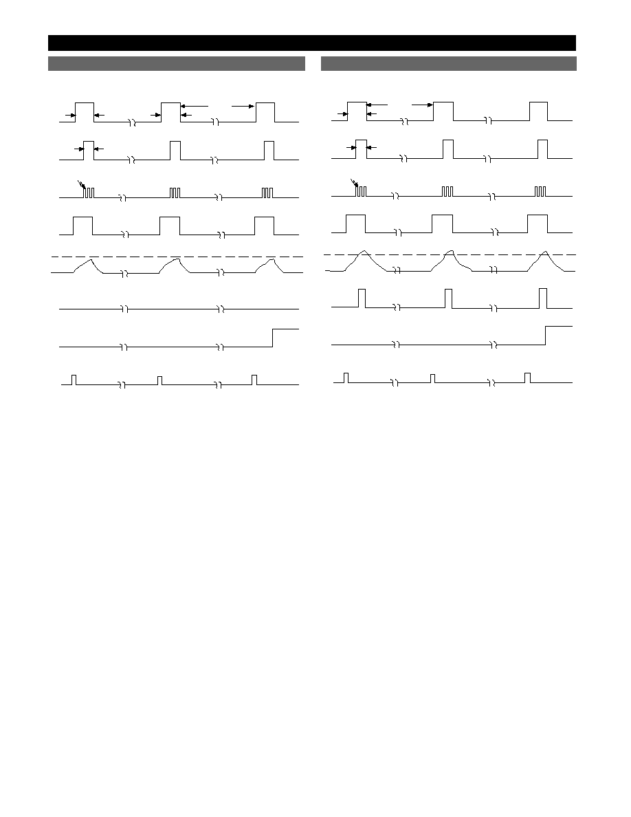
Power Up
20ms
Gate (Clock)
10ms
3.5KHz
Oscillator/
LED Driver
Comp. Ref.
Comp. Ref.
Level
Detector Output
Data Input (low)
Alarm Enable (low)
Preset
10 Sec.
20ms
2 Sec.
Power Up
20ms
Gate (Clock)
10ms
3.5KHz
Oscillator/
LED Driver
Comp. Ref.
Comp. Ref.
Level
Detector Output
Data Input
Alarm Enable
Preset
Timing Diagram In Alarm
Timing Diagram Out of Alarm
Timing Diagrams
CS235
4
CS235
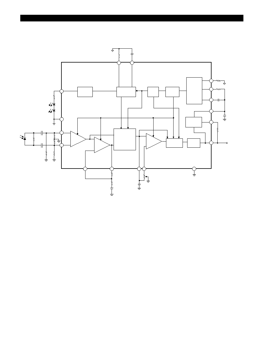
Application Diagram
R4
510
W
C5
.47
mF
R5
100K
Synchronous
Detector
Output
Latch
Clock
Oscillator
LED
Driver
R8
36
W
Status LED
IR LED
Power
UP
Main
Timer
Current
Limit
R6
18k
C3
6.8nF
Gate
C4
.47
mF
R9
270k
1nF
C6
R11
150k
A1
Gain =20
A2
+
4
•
VCC/Output
COMP
CS235
PGnd
-
+
-
1nF
C7
R2
75k
R1
20M
C1
.47
mF
C2
150
mF
R3
6k
LLGnd
R7
12M
Counter
– 3
•
6
5
15
13
14
1
17
18
16
2
3
9
11 10
8
7
R12
150k
R12
150k
R13
150k
5