 | –≠–ª–µ–∫—Ç—Ä–æ–Ω–Ω—ã–π –∫–æ–º–ø–æ–Ω–µ–Ω—Ç: CS2516KN8 | –°–∫–∞—á–∞—Ç—å:  PDF PDF  ZIP ZIP |
Features
OUT
PW
V
CC
Load Switch
C
T
SENSE
R
p
COM
Cycle
Timer
s
Adjustable Battery Sense
from 7 to 12 Volts
s
Pulse Loads Battery at up
to 50mA
s
Standby Current Under
10µA
s
Test Period, Rate and Load
Adjustable
s
On Chip 15mA Output
Driver
Package Options
8L PDIP and 8L SO
CS2516
Pulse-Load Battery Monitor
1
R
P
2
3
4
SENSE
C
T
COM
V
CC
PW
OUT
Load
Switch
8
7
6
5
CS2516
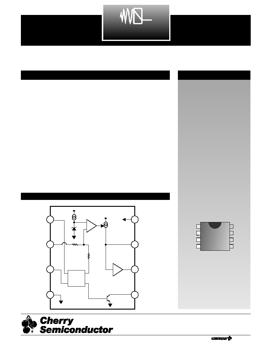
Description
The CS2516 is designed for use in bat-
tery powered medical, security, or
environmental systems where prior
notification of impending power
source failure is a requirement. The IC
effectively provides continuous moni-
toring of battery condition by pulse-
sampling the system voltage at prede-
termined intervals. Low standby cur-
rent permits unswitched connection to
the battery with minimal impact on
operating life. The ability to load the
battery during the test pulse provides
assurance that sufficient reserve capac-
ity exists to operate critical system
components.
The CS2516 contains an internal timer
that generates a 1.0 millisecond test
pulse once each 33 seconds (both times
are typical). The load switch transistor
conducts only during the test pulse,
and can sink up to 50mA directly. An
external transistor can be added to in-
crease the load current capability.
Should, during the test pulse, the sense
terminal voltage fall below the thresh-
old level determined by the internal
(synthesized) temperature compensat-
ed zener diode, the comparator will
permit a charging current to flow out
of PW. This pin is also the input of a
Schmitt trigger that in turn drives the
output transistor. Collectively, the
charge current and trigger, in conjunc-
tion with an external RC network,
operate as a “pulse-stretcher” to pro-
vide output “ON” times that are a
multiple of the sampling time. This
feature permits low battery alarm
devices or visible annunciators to be
driven directly by the IC. The maxi-
mum permissible output current is
30mA.
Block Diagram
1
Cherry Semiconductor Corporation
2000 South County Trail, East Greenwich, RI 02818
Tel: (401)885-3600 Fax: (401)885-5786
Email: info@cherry-semi.com
Web Site: www.cherry-semi.com
A Company
®
Rev. 1/17/95

2
Electrical Characteristics: V
CC
= 9V, R
p
= 9.1 MΩ, C
T
= 4.7µF, Cpw = 0.1µF, Rpw = 10MΩ,
0° ≤ T
A
≤ 85° unless otherwise specified.
PARAMETER
TEST CONDITIONS
MIN
TYP
MAX
UNIT
Absolute Maximum Ratings
Supply Voltage (V
CC
).........................................................................................................................................................0 to 14V
R
p
Input Voltage ............................................................................................................................................................-0.5 to V
CC
SENSE, C
T
, PW, Output and Load Switch....................................................................................................................-0.5 to 8V
Load Current...........................................................................................................................................................................50mA
Output Current ......................................................................................................................................................................30mA
Storage Temperature.................................................................................................................................................-40 to +150˚C
Lead Temperature Soldering: Wave Solder (through hole styles only)..........................................10 sec. max, 260°C peak
Reflow (SMD styles only) ..........................................60 sec. max above 183°C, 230°C peak
CS2516
s V
CC
Operating Voltage
9
12
V
Standby Current
4
10
µA
s Cycle Timer
Charge Current
V
CT
=0V, 6V≤V
CC
≤12V
-1.70
-1.20
-0.48
µA
2V ≤ V
CT
< 7.5V
-0.77
-0.74
-0.71
µA
Discharge Current
V
CT
= 8.8V
8.0
20.0
25.0
mA
V
CT
= 2.0V
1.1
3.0
3.6
mA
Discharge Impedance
4.6V < V
CT
< 8.0V
440
Ω
Upper Charge Threshold
-0.48µA < I
CT
< -1.70µA
7.0
8.0
9.0
V
Lower Charge Threshold
-0.48µA < I
C
< -1.70µA
0.5
1.0
3.0
V
Lower Discharge Threshold
1.1mA < I
C
< 25mA
2.0
4.6
6.0
V
s Load Switch
“ON” Voltage
I
Load Switch
= 50mA
0.3
0.5
V
“OFF” Current
V
Load Switch
= 12V
1.0
µA
s Sense Input
Threshold Voltage
6.3
6.7
7.1
V
Threshold Temp Coefficient
0°C < T
A
< 85°C
150
ppm/°C
Active Impedance
5.0
8.5
12.0
kΩ
s Pulse Stretcher
Source Current
V
SENSE
= 6.3V, V
PW
= 0V
-950
-550
-250
µA
V
CC
=V
SENSE
=6.3V, V
PW
= 0V
-300
-250
-200
µA
Schmitt Upper Threshold
2.25
2.50
2.75
V
Hysteresis
0.60
1.00
1.40
V
Input Bias Current
V
SENSE
=7.1V, V
PW
=1.2V
1.00
µA
s Output Switch
“ON” Voltage
V
PW
= 3V; I
OUT
= 15mA
0.1
0.5
V
“OFF” Current
V
PW
= 0V; V
OUT
= 12V
1.0
µA
3
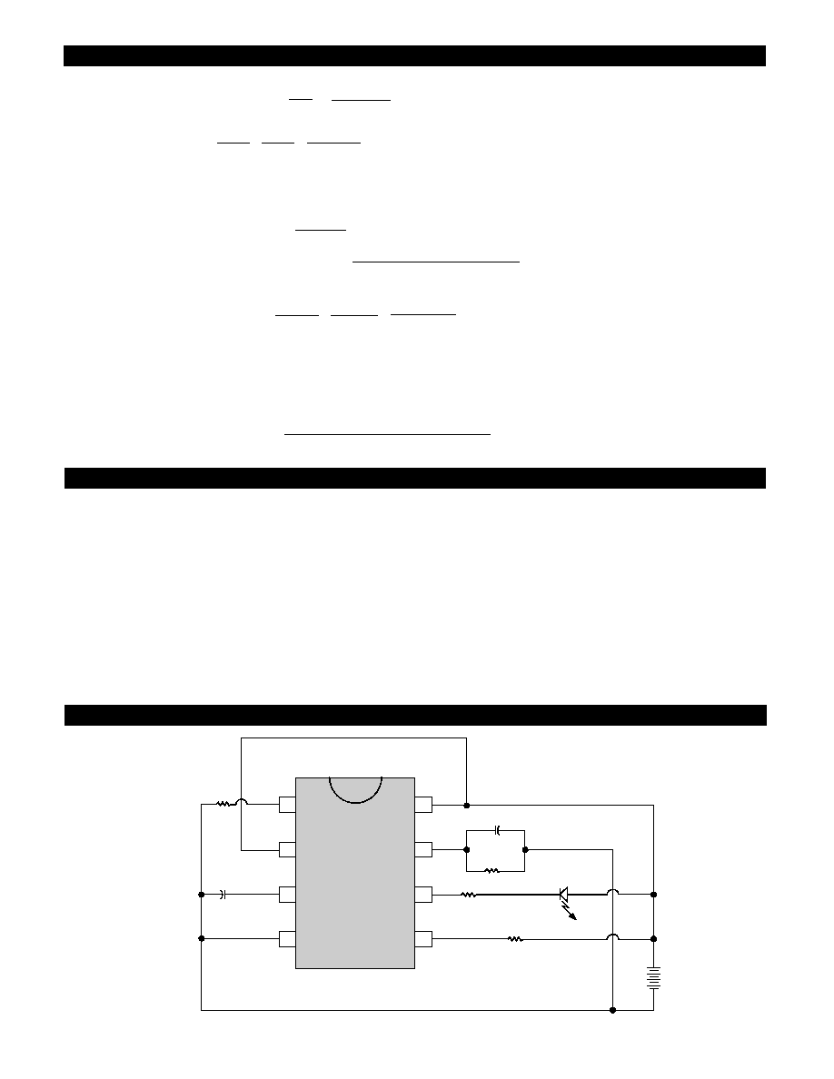
Package Pin Description
PACKAGE PIN #
PIN SYMBOL
FUNCTION
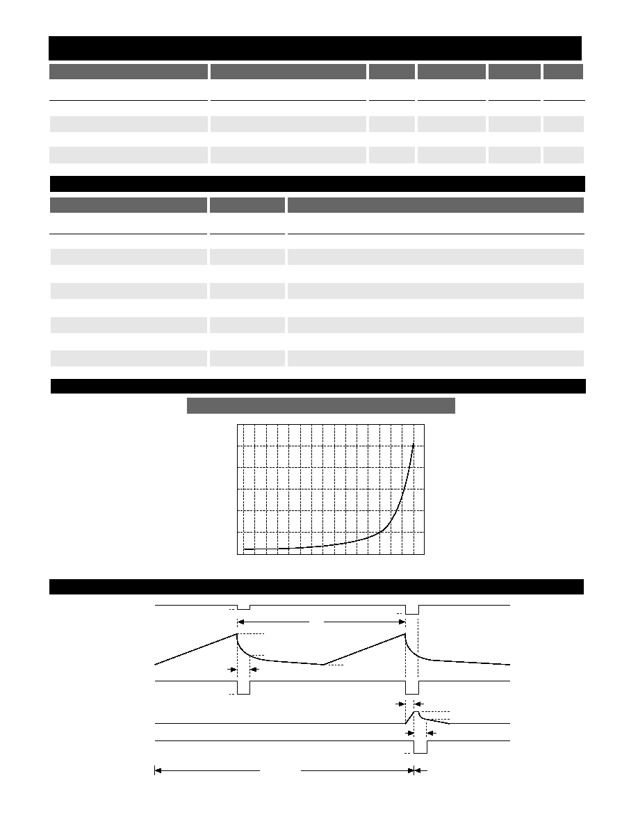
Typical Performance Characteristics
Timing Diagram
C
T
Discharge Impedance vs C
T
Voltage (Typ +25°C)
Electrical Characteristics: V
CC
= 9V, R
P
= 9.1 MΩ, C
T
= 4.7µF, Cpw = 0.1µF, Rpw = 10MΩ,
0° ≤ T
A
≤ 85° unless otherwise specified
PARAMETER
TEST CONDITIONS
MIN
TYP
MAX
UNIT
8.8
8.0
7.0
6.0
5.0
4.0
3.0
2.0
1.0
400
500
600
700
800
900
1000
C
T
Voltage
Impedance,
W
V
CC
C
T
Load
Switch
PW
OUT
BATT. OK
BATT. LOW
0V
1V
0V
1V
V
sat
V
sat
T
pw
510ms
1.5V
2.5V
T
d
1ms
T
p
1.14ms
4.6V
4.6V
8V
1V
7.1V
6.7V
33S
T
t
V
CC
V
CC
V
CC
V
CC
V
CC
CS2516
8L PDIP & SO Narrow
1
R
P
Test period programming resistor.
2
SENSE
Voltage sense comparator input.
3
C
T
Test period, duration programming capacitor.
4
COM
Common negative
5
Load Switch
Collector of pulse loading NPN transistor.
6
OUT
Alarm Pulse width-stretcher output
7
PW
Output pulse-width programming RC.
8
V
CC
Power source.
s Recommended Component Values
Rp Program Resistor
1.0
9.1
MΩ
C
T
Cycle Timer Capacitor
4.7
22.0
µF
C
PW
Pulse Stretcher Capacitor
0.01
0.10
µF
R
PW
Pulse Stretcher Resistor
1
10
MΩ
4
Program and Standby Currents:
I
P
=
=
≈ 1µA Standby Current = 4I
P
= 4µA (typ.)
9V
9.1mΩ
V
CC
R
P
Test Pulse Width:
T
p
= R
d
C
T
x ln(V
P
) ≈ 242C
T
≈ 242 x 4.7µF ≈ 1.14ms
where R
d
is the dynamic cycle timer discharge impedance (440Ω typ.)
and V
P
=
[1n(V
P
) = 0.55 typ.]
Pulse Stretcher: Delay Time:
T
D
=
=
=
≈ 1ms
where V
d
= Schmitt Trigger Upper Threshold (2.5V typ.)
and I
src
= Typical source current at the PW pin at the nominal low battery sense threshold of 6.7V.
Pulse Width: T
p
= C
PW
R
PW
ln(V
S
) ≈ 0.51 x 0.1µF x 10mΩ ≈ 510ms.
and V
S
= [ln(V
S
) = 0.51 typ.]
Schmitt Trigger Upper Threshold
Schmitt Trigger Hysteresis
2.5 x 0.1µF
250µA
2.5C
PW
250µA
V
d
C
PW
I
src
Upper Charge Threshold
Lower Discharge Threshold
V
CC
220
W
C
T
CS2516
R
p
4.7
mF
9.1M
W
9V
PW
OUT
Load Switch
R
p
SENSE
C
T
COM
C
pw
R
pw
10M
W
0.1
mF
+
+
510
W
V
CC
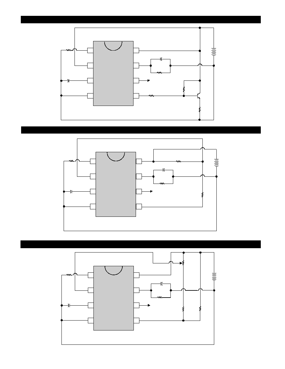
Applications Information
Typical Application Circuit
The value of R
p
affects standby current, operating current,
and the test cycle period. The recommended value is
(V+/1µA) where V+ is the fresh battery voltage. Higher
values of R
p
are not recommended. Minimum recom-
mended value is (V+/10µA) which will increase both the
standby and operating currents by 10X and reduce the test
cycle period by the same factor; the test pulse width will
be unaffected.
The value of C
t
affects both the test cycle period and the
test pulse width. Of critical importance is the selection of a
low leakage type capacitor; if leakage current exceeds the
cycle timer charge current, the timer will not operate.
The pulse stretcher components R
PW
and C
PW
should be
selected such that the delay timer to charge C
PW
is shorter
than the test pulse width programmed by C
t
to guarantee
operation of the Output. The output is an open-collector
transistor which may be used to drive an indicator device
directly or to interface to logic family devices.
The SENSE input typical 8.5kΩ input impedance appears
only during the test pulse; otherwise the SENSE input is in
a high impedance state. The effective low battery thresh-
old voltage can be modified (increased only) by means of a
voltage divider placed across the load resistor. This tech-
nique can also be used to effectively reduce the threshold
tolerance band.
Applications Formulae and Typical Values
CS2516
Cycle Timer Period:
T
t
=
=
=
≈ 33sec.,
where V
t
= Upper Charge Threshold - Lower Charge Threshold (7V typ.)
7 x 4.7µF
1µA
7C
T
1µA
V
T
C
T
I
P
5
V
CC
OUT
C
T
CS-2516
R
p
4.7
mF
9.1M
W
R
L
220
W
9V
PW
OUT
Load Switch
R
p
SENSE
C
T
COM
C
pw
R
pw
10M
W
0.1
mF
+
+
200
W
1.8k
W
Adjustable Sense Threshold
V
CC
OUT
C
T
CS2516
R
p
4.7
mF
9.1M
W
150
W
12V
PW
OUT
Load Switch
R
p
SENSE
C
T
COM
C
pw
R
pw
10M
W
0.1
mF
+
+
51
W
12V Battery Application with 9V Threshold
V
CC
OUT
220
W
C
T
CS2516
R
p
4.7
mF
9.1M
W
820
W
R
L
9V
PW
OUT
Load Switch
R
p
SENSE
C
T
COM
C
pw
R
pw
10M
W
0.1
mF
+
+
Increased Pulse-Load Current Capability
CS2516