 | –≠–ª–µ–∫—Ç—Ä–æ–Ω–Ω—ã–π –∫–æ–º–ø–æ–Ω–µ–Ω—Ç: CS289 | –°–∫–∞—á–∞—Ç—å:  PDF PDF  ZIP ZIP |
Features
Regulator
+
–
V
Z
C
p
–
Gnd
V
SINE
V
BIAS
C
P
+
Pwr Gnd
V
COS
S
Q
IN
F/V OUT
V
CC
V
REG
S
Q
OUT
Function
Generator
Charge
Pump
s
Single Supply Operation
s
On-Chip Regulation
s
20mA Output Drive
Capability
Package Options
20L SOIC Wide
(internally fused leads)
14L PDIP
CS289
20mA Air-Core Tachometer Drive Circuit
1
V
Z
V
SINE
V
BIAS
Gnd
C
P
–
C
P
+
NC
V
CC
V
COS
V
REG
S
Q
IN
S
Q
OUT
F/V
OUT
Gnd
Gnd
Gnd
Gnd
Gnd
Gnd
Gnd
1
V
Z
V
SINE
V
BIAS
Gnd
C
P
–
C
P
+
NC
Pwr Gnd
V
CC
V
COS
V
REG
S
Q
IN
S
Q
OUT
F/V
OUT
CS289
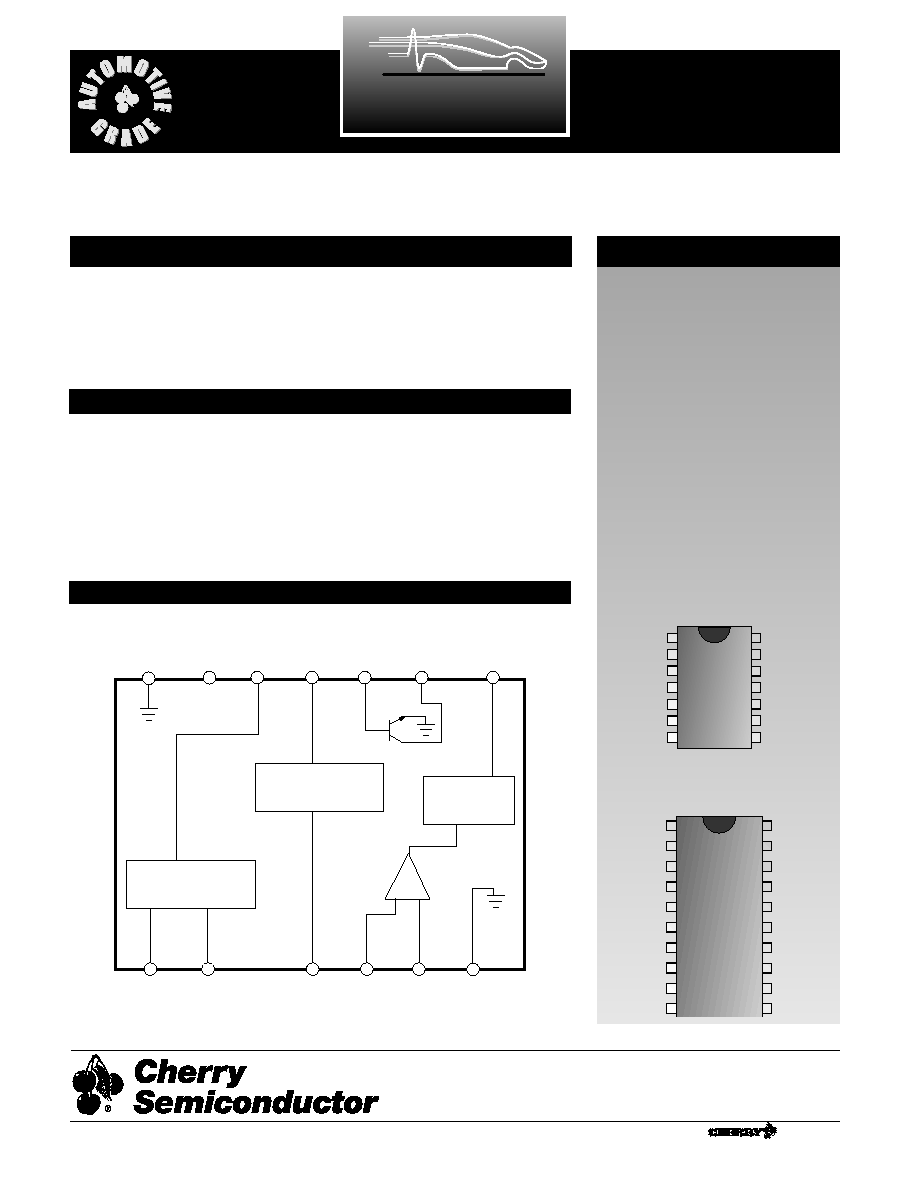
Description
The CS289 is specifically designed
for use with air-core meter move-
ments. The IC has charge pump cir-
cuitry for frequency-to-voltage con-
version, a shunt regulator for stable
operation, a function generator, and
sine and cosine amplifiers. The
buffered sine and cosine outputs
will typically sink or source 20mA.
Block Diagram
Absolute Maximum Ratings
Supply Voltage (V
CC
)......................................................................................20V
Operating Temperature ............................................................–40°C to +100°C
Junction Temperature..................................................................–40°C to 150°C
Storage Temperature.................................................................–65°C to +150°C
Lead Temperature Soldering
Wave Solder (through hole styles only)...........10 sec. max, 260°C peak
Reflow (SMD styles only)............60 sec. max above 183°C, 230°C peak
1
Rev. 3/8/99
Cherry Semiconductor Corporation
2000 South County Trail, East Greenwich, RI 02818
Tel: (401)885-3600 Fax: (401)885-5786
Email: info@cherry-semi.com
Web Site: www.cherry-semi.com
A Company
®

2
Package Pin Description
PACKAGE PIN #
PIN SYMBOL
FUNCTION
Electrical Characteristics: (V
CC
= 13.1V, -30°C ≤ T
A
≤ 85°C)
PARAMETER
TEST CONDITIONS
MIN
TYP
MAX
UNIT
CS289
20L SO
(internally fused leads)
14L PDIP
1
1
V
Z
External Zener reference.
2
2
V
sine
Sine output signal.
3
4
V
BIAS
Test pin or "0" calibration pin.
4, 5, 6, 7,
7
Gnd
Analog Ground connection.
14, 15, 16, 17
8
5
C
P–
Negative input to charge pump.
9
6
C
P+
Positive input to charge pump.
10
3
NC
No Connection
11
8
F/V
OUT
Output voltage proportional to input signal frequency.
Supply Current (Note 2)
V
CC
= 15.0V
54
mA
V
CC
= 13.1V
60
65
mA
V
CC
= 11.3V
60
65
mA
Regulated Voltage
I
REG
= 4.3mA
7.7
8.5
9.3
V
Regulation
I
REG
= 0 to 5mA
0.10
0.20
V
Signal Input Current
T = 25°C
0.1
2.0
4.0
mA
Saturation Voltage
I
SQ
OUT = 5mA, I
SQ
IN = 500µA
0.20
0.55
V
Leakage Current
I
SQ
OUT = 16V, V
SQ
IN = 0V
10
µA
Input Current
C
P
+ = 0, T = 25°C
1
15
nA
F to V Output
V
SQ
IN = 0 (zero input),
∆ = 0°
1.8
2.1
2.4
V
COS
= 0 (Note 1),
∆ = 270°
6.3
7.1
7.9
V
Linearity
E
O
vs. Frequency
V
COS
= 0 (Note 1),
∆ = 270°, T = 25°C
-1.5
1.5
%
V
sine
at
∆ = 0°
V
SQ
IN = 0 (zero input),
∆ = 0°
-0.55
0.00
0.55
V
MAX V
sine+
V
COS
= 0 (Note 1),
∆=90°
3.8
4.5
5.8
V
MAX V
sine-
V
COS
= 0 (Note 1),
∆ = 270°
-3.8
-4.5
-5.8
V
Coil Drive Current
V
COS
= 0 (Note 1),
∆ = 90°, T = 25°C
20
25
mA
V
COS
= 0 (Note 1),
∆ = 270°
20
25
mA
MAX V
COS+
V
SQ
IN = 0 (zero input),
∆ = 0°
3.8
4.5
5.8
V
MAX V
COS-
V
sine
= 0 (Note 1),
∆ = 180°
-3.8
-4.5
-5.8
V
Coil Drive Current
V
SQ
IN = 0 (zero input),
∆ = 0°
20
25
mA
V
sine
= 0 (Note 1),
∆ = 180°
20
25
mA
External Voltage Ref.
4.98
5.40
5.85
V
Note 1: V
sine
measured V
sine
to V
Z
. V
COS
measured V
COS
to V
Z
. All other voltages specified are measured to ground.
Note 2: Max PWR dissipation ≤V
CC
X I
CC
- (V
2
I
sine
+ V12 I
COS
).

3
CS289
Typical Performance Characteristics
V
Z
SINE OUTPUT
+
–
+
–
V
P
COS
Q
V
P
SIN
Q
COSINE
OUTPUT
Q
0
45˚
90˚
135˚
180˚
225˚
270˚
2.1
3
4
5
6
7.1
F/V Output (V)
Relationship of E
Q, Q and Frequency
F/V
OUT
= 2.0V + FREQ X C
T
X R
T
X V
REG
Frequency/Output Angle (
∞)
Output Angle in Polar Form
Charge Pump Output Voltage
V
SINE
, V
COS
(V)
-4.5
-3.5
-2.5
-1.5
V
Z
1.5
2.5
3.5
4.5
4.5V
4.5V
0
45˚
90˚
135˚
180˚
225˚
270˚
V
COS
V
SINE
2.1
3.8
5.45
7.1
Tachometer Angular Deflection (
∞)
Function Generator Output Voltage
Package Pin Description: continued
PACKAGE PIN #
PIN SYMBOL
FUNCTION
Note 1: V
sine
measured V
sine
to V
Z
. V
COS
measured V
COS
to V
Z
. All other voltages specified are measured to ground.
Note 2: Max PWR dissipation ≤V
CC
X I
CC
- (V
2
I
sine
+ V12 I
COS
).
20L SO
14L PDIP
12
9
S
Q
OUT
Buffered square wave output signal.
13
10
S
Q
IN
Speed or RPM input signal.
18
11
V
REG
Voltage regulator output.
19
12
V
COS
Cosine output signal.
20
13
V
CC
Supply voltage.
14
Pwr Gnd
Power Ground connection.

4
CS289
Function Generator Output (
∆): V
CC
=13.1V, T
A
=25°C
∆=ArcTan (Measured angle after calibration at 180°C)
For
∆
A
=45°, 90°, 135°, 180°, 225°, 270°, (Desired angle)
(
∆
A
-
∆
M
)≤4.0°
Temperature Sensitivity: V
CC
=13.1V
∆
∆
MT
=
∆
M
(T=25°C) -
∆M (-20°C≤T≤+85°C)
(∆
∆
MT
)≤3.5°C, -20°C≤T≤+85°C
Voltage Sensitivity: T
A
=25°C
∆
∆
MV
=
∆
M
(V
CC
=13.1V) -
∆
M
(11.3V≤V
CC
≤15V)
(∆
∆
MV
)≤2°, 11.3V≤V
CC
≤15V
V
sine
V
cos
B+
100
W
ZENER
5.4V
SINE
80mH
225
80mH
225
B+
15
18V
Gnd
R2
2k
W
2k
W
1k
W
E
Q
TACH INPUT
R
T
180k
W
*
C
OUT
1
mF
±10%
R1
1k
W
C
T
0.01
mF
S
Q
OUT
F-V
OUT
NC
C
P
–
V
Z
V
SINE
V
BIAS
Gnd
* ADJUST FOR TRIMMING
V
CC
V
COS
V
REG
S
Q
IN
C
P
+
CS289
Figure 1. Functional Diagram of CS289 Circuit.
The input frequency is buffered through a transistor, then
applied to the charge pump for frequency-to-voltage con-
version (Figure 1). The charge pump output voltage, E
∆,
will range from 2.1V with no input (
∆= 0°) to 7.1V at ∆ =
270°. The charge that appears on C
T
is reflected to C
OUT
through a Norton amplifier. The frequency applied at
S
Q
IN charges and discharges C
T
through R
1
and R
2
. C
OUT
reflects the charge as a voltage across resistor R
T
.
Circuit Description
Charge Pump
Function Generator/Sine and Cosine Amplifiers
The output waveforms of the sine and cosine amplifiers
are derived by On-Chip Amplifier/Comparator circuitry.
The various trip points for the circuit (i.e. 90°, 180°, 270°)
are determined by an internal resistor divider connected
to the voltage regulator. The voltage E
∆ is compared to
the divider network by the function generator circuitry.
Use of an external zener reference at V
Z
allows both sine
and cosine amplifiers to swing positive and negative with
respect to this reference. The output magnitudes and
directions have the relationship as shown in Typical
Characteristics diagrams.
Note: Pin connections referenced are for the 14L DIP.
5
I
IN
0.7V
2.1V
I
OUT/E
Q
C
P
–
C
P
+
Gnd
F-V
OUT
C
P
R
T
V
BIAS
C
P
–
C
P
+
Gnd
V
REG
S
Q
IN
S
Q
OUT
F-V
OUT
NC
V
COS
R
T
C
T
1k
W
10k
W
TRIM
C
P
V
F/V
OUT
= 2.1 + Frequency x C
T
x R
T
(V
REG
-0 .7)
The above equations were used in calculating the follow-
ing values, where V
F/V
OUT
= 7.1V at =270° and C
T
= 0.01 F.
4 cylinder: Freq = 200Hz, R
T
= 320kΩ
6 cylinder: Freq = 300Hz, R
T
= 220kΩ
8 cylinder: Freq = 400Hz, R
T
= 150kΩ
CS289
Tachometer Application
RPM
60
x # OF CYL.
2
= Frequency
Typical values shown above apply to a nominal value of
V
REG
of 8.5 volts. It must be realized that trimming of R
T
will be necessary to compensate for variations in regula-
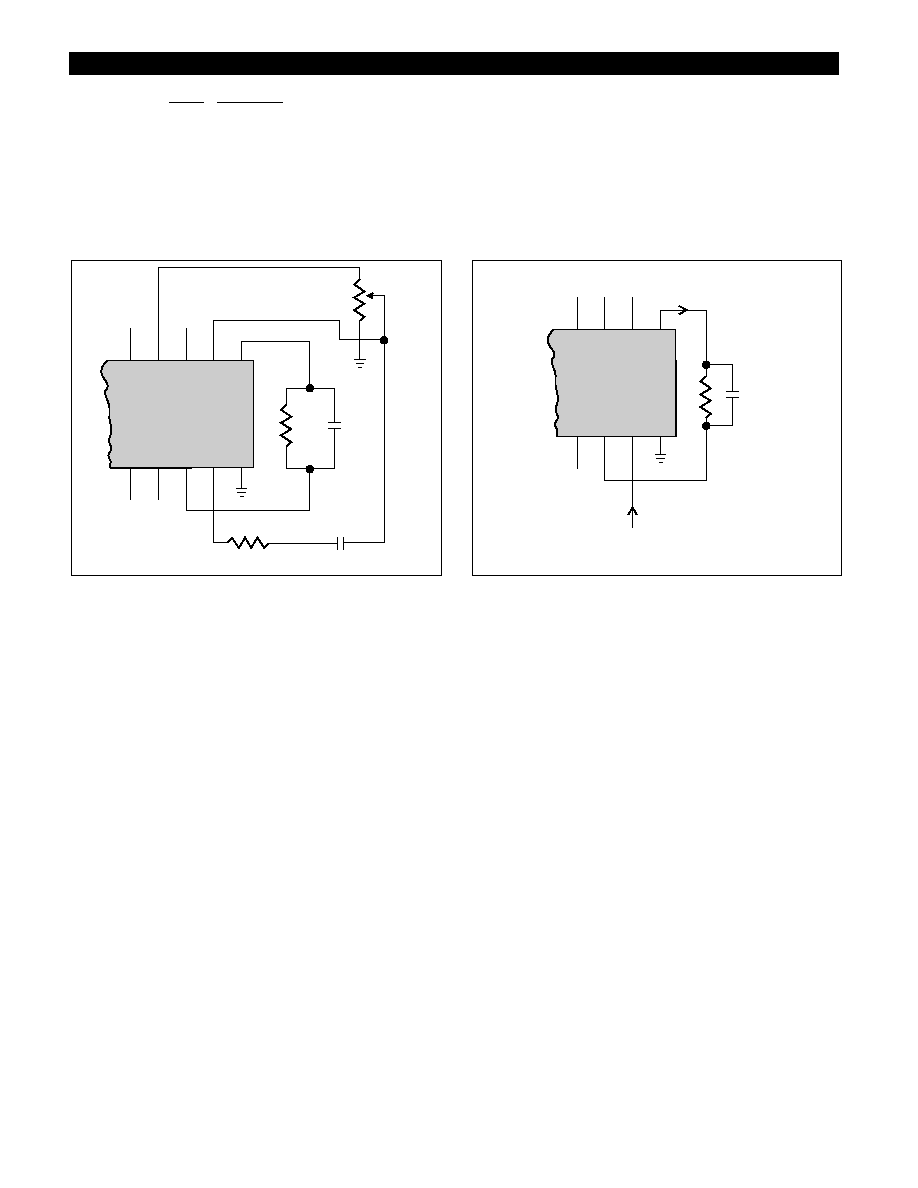
tor voltage from one unit to another.
An alternative to this adjustment is to replace R
2
with a
potentiometer, as shown in Figure 2.
Partial schematic shown in Figure 3 represents one met-
hod for use with DC applications instead of frequency.
Figure 2: Alternate Trimming Method
Figure 3: DC Application