1
Features
Device
Driver
Gnd
Sense
VCC
OSC
IGN
ENABLE
Series
Regulator
VSUP
LAMP
VREG
Lamp
Indicator
OSC
VHV
+
≠
RS Flop
Set
Dominate
S
R
Q
R
ENABLE
STATOR
Power Up
STATOR
Timer
VSUP
Load Dump
Detection and
Protection
Note:
CS-3341/CS-387 Disconnected
CS-3351/CS-386 Connected
+
≠
DELAY
SC
STATOR
+
≠
VSUP
s
Drives NPN Darlington
s
Short Circuit Protection
s
80V Load Dump
s
Temperature Compensated
Regulation Voltage
s
Shorted Field Protection
Duty Cycle, Self Clearing
Package Options
CS3341/3351/386/387
Alternator Voltage Regulator
Darlington Driver
CS3341/51
CS386/387
Description
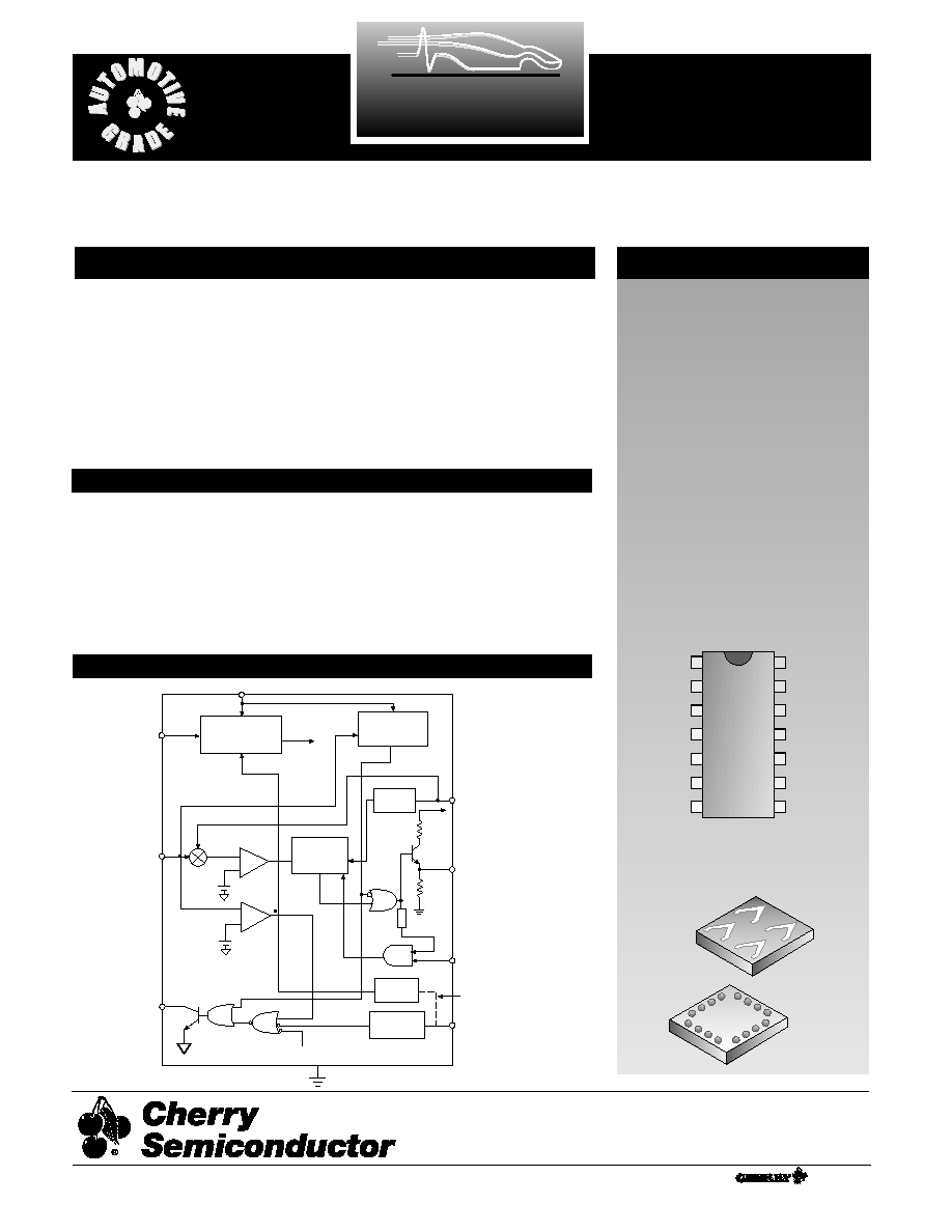
The CS3341/3351/386/387 integral
alternator regulator integrated cir-
cuit provides the voltage regulation
for automotive, 3-phase alternators.
It drives an external power
Darlington for control of the alter-
nator field current. In the event of a
charge fault, a lamp output pin is
provided to drive an external dar-
lington transistor capable of switch-
ing on a fault indicator lamp. An
overvoltage or no STATOR signal
condition activates the lamp output.
The CS3341 and CS3351 are avail-
able in SO14 packages. The CS386
and CS387 are available as Flip Chips.
Block Diagram
Absolute Maximum Ratings
Storage Temperature Range .....................................................-55∞C to +165∞C
Junction Temperature Range ....................................................-40∞C to +150∞C
Continuous Supply..........................................................................................27V
I
CC
Load Dump .........................................................................................400 mA
Lead Temperature Soldering
Reflow (SMD styles only)............60 sec. max above 183∞C, 230∞C peak
1
DD
Gnd
NC
OSC
Lamp
NC
NC
SC
NC
V
CC
Sense
IGN
STATOR
NC
14 Lead SO
Flip Chip
CS3341/51
CS386/387
A Company
Æ
Rev. 4/15/99
Cherry Semiconductor Corporation
2000 South County Trail, East Greenwich, RI 02818
Tel: (401)885-3600 Fax: (401)885-5786
Email: info@cherry-semi.com
Web Site: www.cherry-semi.com
2
Electrical Characteristics: CS3341/51: -40∞C < T
A
< 125∞C; -40∞C < T
J
< 150∞C, 9V V
CC
17V;
unless otherwise specified
PARAMETER
TEST CONDITIONS
MIN
TYP
MAX
UNIT
CS3341/3351/386/387
s
Supply
Supply Current Enabled
≠
12
25
mA
Supply Current Disabled
≠
50
µA
s
Driver Stage
Device Driver
≠
≠
≠
Output High Current
V
DD
= 1.2V
-10
-6
-4
mA
Output Low Voltage
I
OL
= 25µA
≠
0.35
V
Minimum ON Time
200
µs
Minimum Duty Cycle
≠
6
10
%
Short Circuit Duty Cycle
1
5
%
Field Switch Turn On
Rise Time
30
90
µs
Fall Time
30
90
µs
s
Stator
Input High Voltage
10
V
Input Low Voltage
≠
6
V
Stator Time Out
High to Low
6
100
600
ms
Stator Power-Up Input High
CS3351/386 only
10
≠
V
Stator Power-Up Input Low
CS3351/386 only
≠
6
V
s
Lamp
Output High Current
V
LAMP
@ 3V
≠
50
µA
Output Low Voltage
I
LAMP
@ 30mA
≠
0.35
V
s
Ignition
Input High Voltage
I
CC
> 1mA
1.8
≠
V
Input Low Voltage
I
CC
< 100µA
≠
0.5
V
s
Oscillator
Oscillator Frequency
C
OSC
= 0.22µF
65
325
Hz
Rise Time/Fall Time
C
OSC
= 0.22µF
17
≠
≠
Oscillator High Threshold
C
OSC
= 0.22µF
≠
6
V
s
Battery Sense
Input Current
-10
+10
µA
Regulation Voltage
@25∞C, R
1
= 100k, R
2
= 50k
13.5
16.0
V
Proportional Control
0.050
0.400
V
High Voltage
V
High Voltage
@ Lamp On
1.083
1.190
Threshold Ratio
V
Regulation
@ 50% Duty Cycle
High Voltage Hysteresis
0.020
0.600
V
3
CS3341/3351/386/387
Package Pin Description
PACKAGE PIN #
PIN SYMBOL
FUNCTION
14L SO
Flip Chip
1
1
Driver
Output driver for external power switch-Darlington.
2
2
Gnd
Ground.
3, 6, 7, 9, 13
3
NC
No connection.
4
4
OSC
Timing capacitor for oscillator.
5
5
Lamp
Base driver for lamp driver indicates no stator signal or over-
voltage condition.
8
6
IGN
Switched ignition power up.
10
7
Stator
Stator signal input for stator timer (CS3351 also power up).
11
8
Sense
Battery sense voltage regulator comparator input and
protection.
12
9
V
CC
Supply for IC.
14
10
SC
Short circuit sensing.
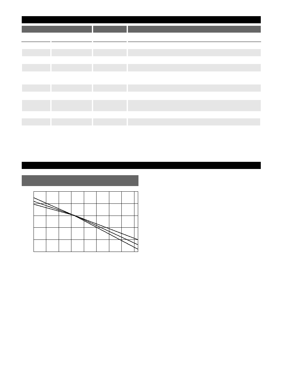
Typical Performance Characteristics
15.5
15
14.5
14
13.5
13
Battery V
oltage
Temperature (
∞
C)
-
40
-
20
0
20
40
60
80
100
120
CS3341/3351 Battery Voltage vs Temperature (∞C)
Over Process Variation
4
CS3341/3351/386/387
Application Information
R2
10k
SC
Driver
Gnd
STATOR
Sense
V
CC
OSC
IGN
20k
C4
0.022
µ
F
50k
C3
.047
µ
F
100k
250
C1
0.1
µ
F
18k
BATTERY
LAMP
2.4k
10
Power
Darlington
Lamp
Indicator
IGNITION
SWITCH
POWER GROUND
Power Darlington
FIELD
R5
R4
R3
R1
R6
R9
R7
R10
510
STATOR
RECTIFIER
A
F
I
S
D1
Q1
*
C2
10
µ
F
*
Note: C2 optional for reduced jitter.
Figure 2. Typical Application Diagram
The CS3341 and CS3351 IC's are designed for use in an
alternator charging system. The circuit is also available in
flip-chip form as the CS387 and CS386.
In a standard alternator design (Figure 1), the rotor carries
the field winding. An alternator rotor usually has several N
and S poles. The magnetic field for the rotor is produced by
forcing current through a field or rotor winding. The Stator
windings are formed into a number of coils spaced around
a cylindrical core. The number of coils equals the number
of pairs of N and S poles on the rotor. The alternating cur-
rent in the Stator windings is rectified by the diodes and
applied to the regulator. By controlling the amount of field
current, the magnetic field strength is controlled and hence
the output voltage of the alternator.
Referring to Figure 2, a typical application diagram, the
oscillator frequency is set by an external capacitor connect-
ed between OSC and ground. The sawtooth waveform
ramps between 1V and 3V and provides the timing for the
system. For the circuit shown the oscillator frequency is
approximately 140Hz. The alternator voltage is sensed at
Terminal A via the resistor divider network R1/R2 on the
Sense pin of the IC. The voltage at the sense pin determines
the duty cycle for the regulator. The voltage is adjusted by
potentiometer R2. A relatively low voltage on the sense
pin causes a long duty cycle that increases the Field cur-
rent. A high voltage results in a short duty cycle.
The ignition Terminal (I) switches power to the IC through
the V
CC
pin. In the CS3351/CS386, the Stator pin senses the
voltage from the stator. This will keep the device powered
while the voltage is high, and it also senses a stopped
engine condition and drives the Lamp pin high after the
stator timeout expires. The Lamp pin also goes high when
an overvoltage condition is detected on the sense pin. This
causes the darlington lamp drive transistor to switch on
and pull current through the lamp. If the system voltage
continues to increase, the field and lamp output turn off as
in an overvoltage or load dump condition.
The SC or Short Circuit pin monitors the field voltage. If
the drive output and the SC voltage are simultaneously
high for a predetermined period, a short circuit condition
is assumed and the output is disabled. The regulator is
forced to a minimum short circuit duty cycle.
BATTERY
Lamp
Indicator
IGNITION
SWITCH
Regulator
I
Gnd
FIELD
A
S
FIELD Winding
STATOR
Winding
Figure 1. IAR System Block Diagram

5
CS3341/3351/386/387
Package Specification
Thermal Data
14L SO
R
JC
typ
30
∞C/W
R
JA
typ
125
∞C/W
D
Lead Count
Metric
English
Max
Min
Max
Min
14L SO
8.75
8.55
.344
.337
PACKAGE DIMENSIONS IN mm (INCHES)
PACKAGE THERMAL DATA
Surface Mount Narrow Body (D); 150 mil wide
1.27 (.050) BSC
0.51 (.020)
0.33 (.013)
6.20 (.244)
5.80 (.228)
4.00 (.157)
3.80 (.150)
1.57 (.062)
1.37 (.054)
D
0.25 (0.10)
0.10 (.004)
1.75 (.069) MAX
1.27 (.050)
0.40 (.016)
REF: JEDEC MS-012
0.25 (.010)
0.19 (.008)