1
Features
V
CC
Gnd
OSC
V
FB
COMP
Sense
V
REF
V
OUT
Output
Enable
5V
Reference
Internal
Bias
NOR
S
R
PWM
Latch
Current
Sensing
Comparator
Oscillator
1 V
R
2 R
V
C
Error
Amplifier
+
≠
2.50V
Set/
Reset
Undervoltage
Lock-out Circuit
34V
( ) Indicates CS-2843A/3843A
16V/10V
(8.4V/7.6V)
V
CC
Pwr
Pwr Gnd
s
Optimized for Off-line
Control
s
Internally Trimmed
Temperature
Compensated Oscillator
s
Maximum Duty-cycle
Clamp
s
V
REF
stabilized before
Output Stage is Enabled
s
Low Start-up Current
s
Pulse-by-pulse Current
Limiting
s
Improved Undervoltage
Lockout
s
Double Pulse Suppression
s
1% Trimmed Bandgap
Reference
s
High Current Totem Pole
Output
Package Options
CS2842A/3843A SERIES
Off-Line Current Mode PWM Control
Circuit with Undervoltage Lockout
CS2842A/CS3842A
CS2843A/CS3843A
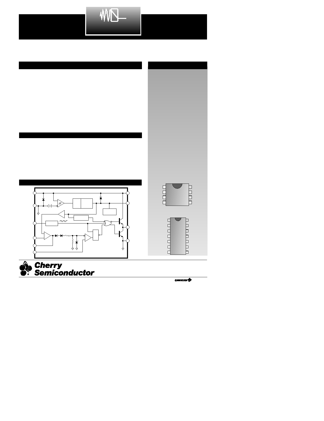
Description
Block Diagram
Absolute Maximum Ratings
Supply Voltage (I
CC
<30mA).........................................................................Self Limiting
Supply Voltage (Low Impedance Source) .................................................................30V
Output Current..............................................................................................................±1A
Output Energy (Capacitive Load) ................................................................................5µJ
Analog Inputs (V
FB
, Sense) ...........................................................................-0.3V to 5.5V
Error Amp Output Sink Current .............................................................................10mA
Lead Temperature Soldering
Wave Solder (through hole styles only) ..........10 sec. max, 260∞C peak
Reflow (SMD styles only) ...........60 sec. max above 183∞C, 230∞C peak
1
COMP
2
3
4
V
FB
Sense
OSC
V
REF
V
CC
V
OUT
Gnd
8
7
6
5
8 Lead PDIP & SO Narrow
10
7
14
13
12
8
1
2
3
4
5
6
11
9
COMP
NC
V
FB
NC
Sense
NC
OSC
V
REF
NC
V
CC
V
CC
Pwr
V
OUT
Pwr Gnd
Gnd
14 Lead SO Narrow
The CS284XA, CS384XA provides all
the necessary features to implement
off-line fixed frequency current-mode
control with a minimum number of
external components.
The CS384XA family incorporates a
new precision temperature-controlled
oscillator with an internally trimmed
discharge current to minimize varia-
tions in frequency. A precision duty-
cycle clamp eliminates the need for an
external oscillator when a 50% duty-
cycle is used. Duty-cycles greater than
50% are also possible. On board logic
ensures that V
REF
is stabilized before
the output stage is enabled. Ion
implant resistors provide tighter con-
trol of undervoltage lockout.
Other features include low start-up
current, pulse-by-pulse current limit-
ing, and a high-current totem pole out-
put for driving capacitive loads, such
as the gate of power MOSFET. The out-
put is LOW in the off state, consistent
with N-channel devices.
The CS384XA series of current-mode
control ICs are available in 8 and14
lead packages for surface mount (SO)
applications as well as 8 lead PDIP
packages.
A Company
Æ
Rev. 10/23/98
Cherry Semiconductor Corporation
2000 South County Trail, East Greenwich, RI 02818
Tel: (401)885-3600 Fax: (401)885-5786
Email: info@cherry-semi.com
Web Site: www.cherry-semi.com

2
Electrical Characteristics:
-25∞ T
A
85∞C for CS2842A/2843A, 0∞ T
A
70∞C for CS3842A/3843A. V
CC
= 15V (Note 1);
R
T
= 680, C
T
= .022µF for triangular mode, R
T
= 10k, C
T
= 3.3nF for sawtooth mode (see Figure 3), unless otherwise stated.
CS2842A/CS2843A CS3842A/CS3843A
PARAMETER
TEST CONDITIONS
MIN
TYP
MAX
MIN
TYP
MAX UNITS
CS2842A/3843A SERIES
s
Reference Section
Output Voltage
T
J
= 25∞C, I
OUT
= 1mA
4.95
5.00
5.05
4.90
5.00
5.10 V
Line Regulation
12 V
IN
25V
6
20
6
20
mV
Load Regulation
1 I
OUT
20mA
6
25
6
25
mV
Temperature Stability
(Note 2)
0.2
0.4
0.2
0.4
mV/∞C
Total Output Variation
Line, Load, Temp. (Note 2)
4.90
5.10
4.82
5.18 V
Output Noise Voltage
10Hz f 10kHz, T
J
= 25∞C (Note 2)
50
50
µV
Long Term Stability
T
A
= 125∞C, 1kHrs. (Note 2)
5
25
5
25
mV
Output Short Circuit
T
A
= 25∞C
-30
-100
-180
-30
-100
-180 mA
s
Oscillator Section
Initial Accuracy
Sawtooth Mode (see Fig. 3), T
J
= 25∞C 47
52
57
47
52
57
kHz
Triangular Mode (see Fig. 3), T
J
= 25∞C 47
52
57
44
52
60
kHz
Voltage Stability
12 V
CC
25V
0.2
1.0
0.2
1.0
%
Temp. Stability
Sawtooth Mode T
MIN
T
A
T
MAX
(Note 2)
5
5
%
Triangular Mode T
MIN
T
A
T
MAX
(Note 2)
8
8
%
Amplitude
OSC peak to peak
1.7
1.7
V
Discharge Current
T
J
= 25∞C
7.5
8.3
9.3
7.5
8.3
9.3
mA
T
MIN
T
A
T
MAX
7.2
9.5
7.2
9.5
mA
s
Error Amp Section
Input Voltage
V
COMP
= 2.5V
2.45
2.50
2.55
2.42
2.50
2.58 V
Input Bias Current
V
FB
= 0
-0.3
-1.0
-0.3
-2.0 µA
A
VOL
2 V
OUT
4V
65
90
65
90
dB
Unity Gain Bandwidth
(Note 2)
0.7
1.0
0.7
1.0
MHz
PSRR
12 V
CC
25V
60
70
60
70
dB
Output Sink Current
V
FB
= 2.7V, V
COMP
= 1.1V
2
6
2
6
mA
Output Source Current
V
FB
= 2.3V, V
COMP
= 5V
-0.5
-0.8
-0.5
-0.8
mA
V
OUT
High
V
FB
= 2.3V, R
L
= 15k to ground
5
6
5
6
V
V
OUT
Low
V
FB
= 2.7V, R
L
= 15k to V
REF
0.7
1.1
0.7
1.1
V
s
Current Sense Section
Gain
(Notes 3 & 4)
2.85
3.00
3.15
2.85
3.00
3.15 V/V
Maximum Input Signal
V
COMP
= 5V (Note 3)
0.9
1.0
1.1
0.9
1.0
1.1
V
PSRR
12 V
CC
25V (Note 3)
70
70
dB
Input Bias Current
V
Sense
= 0
-2
-10
-2
-10
µA
Delay to Output
T
J
= 25∞C (Note 2)
150
300
150
300
ns
s
Output Section
Output Low Level
I
SINK
= 20mA
0.1
0.4
0.1
0.4
V
I
SINK
= 200mA
1.5
2.2
1.5
2.2
V
Output High Level
I
SOURCE
= 20mA
13.0
13.5
13.0
13.5
V
I
SOURCE
= 200mA
12.0
13.5
12.0
13.5
V
3
CS2842A/3843A SERIES
Electrical Characteristics: continued
CS2842A/CS2843A CS3842A/CS3843A
PARAMETER
TEST CONDITIONS
MIN
TYP
MAX
MIN
TYP
MAX UNITS
CS2842A
CS3842A
CS2843A/CS3843A
PARAMETER
TEST CONDITIONS
MIN
TYP
MAX
MIN
TYP
MAX MIN
TYP
MAX UNITS
Notes:
1. Adjust V
CC
above the start threshold before setting at 15V.
3. Parameter measured at trip point of latch with VFB=0.
2.These parameters, although guaranteed, are not 100% tested in production.
4. Gain defined as:
A =
; 0 VSense 0.8V.
V
COMP
V
Sense
s
Under-Voltage Lockout Section
Start Threshold
15
16
17
14.5
16.0 17.5
7.8
8.4
9.0
V
Min. Operating After Turn On
9
10
11
8.5
10.0 11.5
7.0
7.6
8.2
V
Voltage
s
Output Section: continued
Rise Time
T
J
= 25∞C, C
L
= 1nF (Note 2)
50
150
50
150
ns
Fall Time
T
J
= 25∞C, C
L
= 1nF (Note 2)
50
150
50
150
ns
Output Leakage
UVLO Active, V
OUT
= 0
-0.01
-10.00
-0.01 -10.00 µA
s
Total Standby Current
Start-Up Current
0.5
1.0
0.5
1.0
mA
Operating Supply Current
V
FB
= V
Sense
= 0V, R
T
= 10k, C
T
= 3.3nF 11
17
11
17
mA
V
CC
Zener Voltage
I
CC
= 25mA
34
34
V
Package Pin Description
PACKAGE PIN #
PIN SYMBOL
FUNCTION
8L PDIP/SO
14L SO Narrow
1
1
COMP
Error amp output, used to compensate error amplifier
2
3
V
FB
Error amp inverting input
3
5
Sense
Noninverting input to Current Sense Comparator
4
7
OSC
Oscillator timing network with Capacitor to Ground, resistor
to V
REF
5
8
Gnd
Ground
9
Pwr Gnd
Output driver Ground
6
10
V
OUT
Output drive pin
11
V
CC
Pwr
Output driver positive supply
7
12
V
CC
Positive power supply
8
14
V
REF
Output of 5V internal reference
2,4,6,13
NC
No Connection
4
CS2842A/3843A SERIES
V
REF
V
CC
V
OUT
1k
1W
0.1
µ
F
0.1
µ
F
V
REF
V
CC
V
OUT
Gnd
V
FB
Sense
OSC
COMP
5k
100k
4.7k
1k
ERROR AMP
ADJUST
4.7k
Sense
ADJUST
R
T
2N2222
C
T
Gnd
A
Test Circuit
Undervoltage Lockout
During Undervoltage Lockout (Figure 1), the output driv-
er is biased to a high impedance state. The output should
be shunted to ground with a resistor to prevent output
leakage current from activating the power switch.
PWM Waveform
To generate the PWM waveform, the control voltage from
the error amplifier is compared to a current sense signal
which represents the peak output inductor current (Figure
2). An increase in V
CC
causes the inductor current slope to
increase, thus reducing the duty cycle. This is an inherent
feed-forward characteristic of current mode control, since
the control voltage does not have to change during
changes of input supply voltage.
When the power supply sees a sudden large output cur-
rent increase, the control voltage will increase allowing the
duty cycle to momentarily increase. Since the duty cycle
tends to exceed the maximum allowed to prevent trans-
V
CC
ON/OFF Command
to reset of IC
V
ON
16V 8.4V
V
OFF
10V 7.6V
CSX842A CSX843A
<15mA
<1mA
V
ON
V
OFF
I
CC
V
CC
Circuit Description
Typical Performance Characteristics
.0005
.001
.002
.003
.005
.01
.02
.03 .04
800
900
FREQ. (kHz)
C
T
(
µ
F)
700
600
500
400
300
200
100
.05
R
T
=1.5k
R
T
=680
R
T
=10k
100
200
700
1k
2k
5k
7k
10k
80
90
DUTY
CYCLE (%)
R
T
(
)
70
60
50
40
30
20
10
4k
3k
500
400
300
100
Oscillator Duty Cycle vs R
T
Oscillator Frequency vs C
T
Figure 1: Typical Undervoltage Characteristics
5
CS2842A/3843A SERIES
former saturation in some power supplies, the internal
oscillator waveform provides the maximum duty cycle
clamp as programmed by the selection of oscillator com-
ponents.
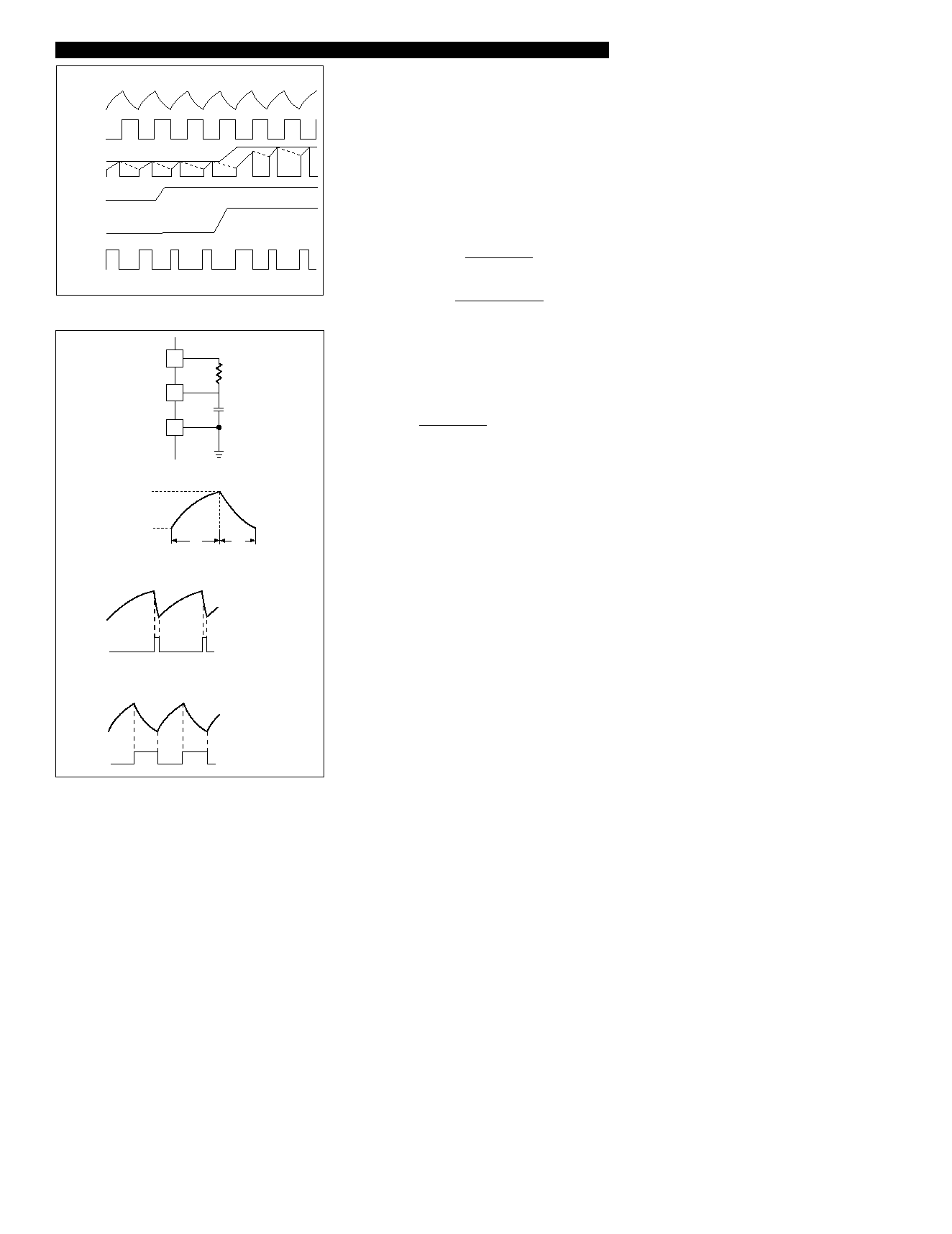
Setting the Oscillator
Oscillator timing capacitor, C
T
, is charged by V
REF
through
R
T
and discharged by an internal current source. During
the discharge time, the internal clock signal blanks out the
output to the Low state, thus providing a user selected
maximum duty cycle clamp. Charge and discharge times
are determined by the formula:
t
c
= R
T
C
T
ln
t
d
= R
T
C
T
ln
Substituting in typical values for the parameters in the
above formulas:
V
REF
= 5.0V, V
upper
= 2.7V, V
lower
= 1.0V, I
d
= 8.3mA
t
c
0.5534R
T
C
T
t
d
= R
T
C
T
ln
The frequency and maximum duty cycle can be deter-
mined using the Typical Performance Characteristic
graphs.
Grounding
High peak currents associated with capacitive loads neces-
sitate careful grounding techniques. Timing and bypass
capacitors should be connected close to Gnd pin in a sin-
gle point ground.
The transistor and 5k potentiometer, shown in the test
circuit, are used to sample the oscillator waveform and
apply an adjustable ramp to
Sense
.
)
2.3 - 0.0083 R
T
4.0 - 0.0083 R
T
(
)
V
REF
- I
d
R
T
- V
lower
V
REF
- I
d
R
T
- V
upper
(
)
V
REF
- V
lower
V
REF
- V
upper
(
V
REF
OSC
Gnd
R
T
C
T
Circuit Description: continued
V
OSC
Internal Clock
LARGE R
T
(
10k
)
V
REF
Internal Clock
SMALL R
T
(
700k
)
Sawtooth Mode
Triangular Mode
V
upper
V
lower
t
c
t
d
V
CC
I
OUT
V
OUT
Switch
Current
EA Output
V
OSC
OSC
RESET
Figure 2: Timing Diagram for key CS2841B parameters
Figure 3: Oscillator Timing Network and parameters
Timing parameters
Thermal Data
8 L
8 L
14 L
PDIP
SO Narrow SO Narrow
R
JC
typ
52
45
30
∞C/W
R
JA
typ
100
165
125
∞C/W
6
Ordering Information
Part Number
0∞C to
-25∞C to
Description
70∞C
85∞C
CS2842ALN8
∑
8L PDIP
CS2843ALN8
∑
8L PDIP
CS3842AGN8
∑
8L PDIP
CS3842AGD8
∑
8L SO Narrow
CS3842AGDR8
∑
8L SO Narrow
(tape & reel)
CS3842AGD14
∑
14L SO Narrow
CS3842AGDR14
∑
14L SO Narrow
(tape & reel)
CS2843ALD14
∑
14L SO Narrow
CS2843ALDR14
∑
14L SO Narrow
(tape & reel)
CS3843AGN8
∑
8L PDIP
CS3843AGD8
∑
8L SO Narrow
CS3843AGDR8
∑
8L SO Narrow
(tape & reel)
CS3843AGD14
∑
14L SO Narrow
CS3843AGDR14
∑
14L SO Narrow
(tape & reel)
Rev. 10/23/98
CS2842A/3843A SERIES
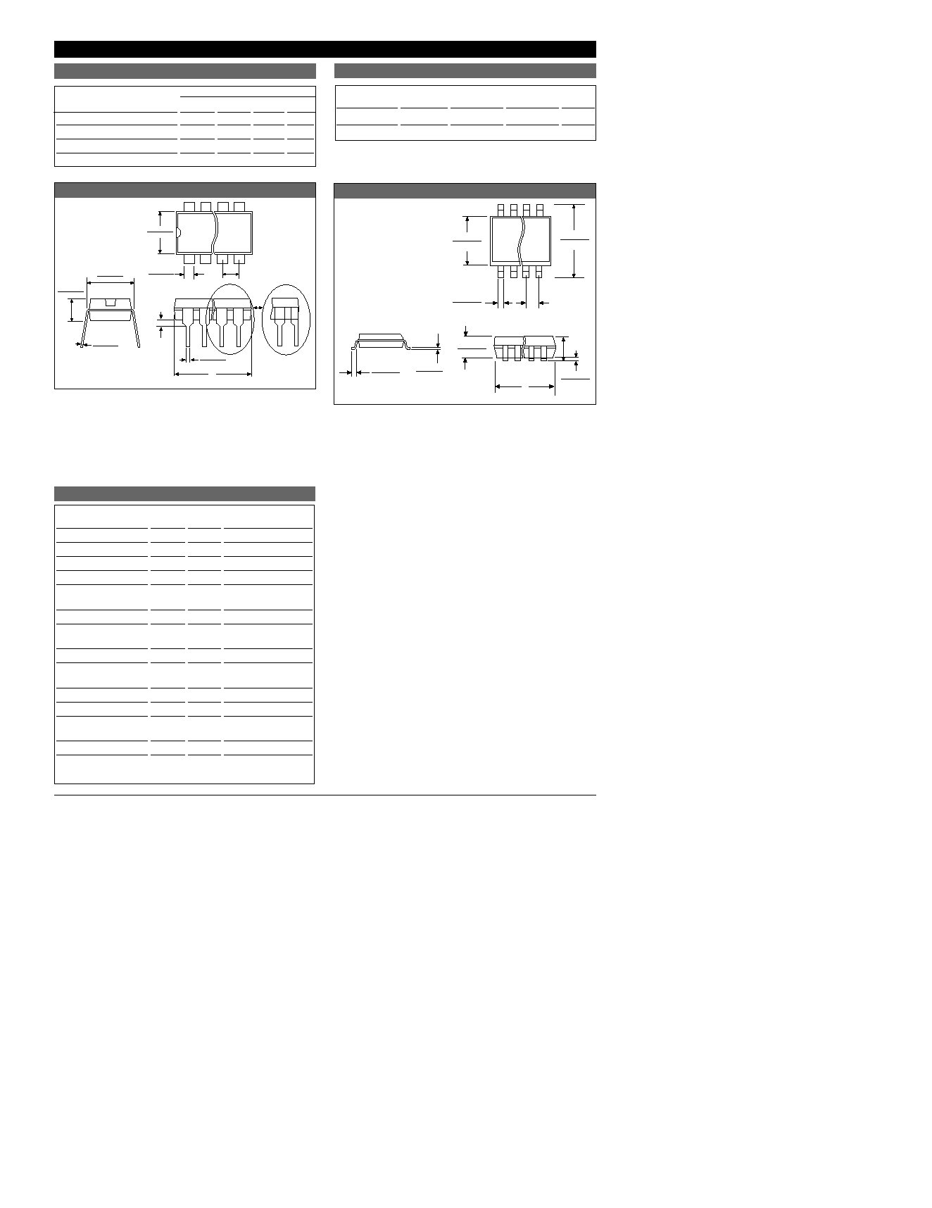
D
Lead Count
Metric
English
Max
Min
Max
Min
8 Lead PDIP
10.16
9.02
.400
.355
8 Lead SO Narrow
5.00
4.80
.197
.189
14 Lead SO Narrow
8.75
8.55
.344
.337
Package Specification
PACKAGE DIMENSIONS IN mm (INCHES)
PACKAGE THERMAL DATA
© 1999 Cherry Semiconductor Corporation
Cherry Semiconductor Corporation reserves the
right to make changes to the specifications without
notice. Please contact Cherry Semiconductor
Corporation for the latest available information.
Plastic DIP (N); 300 mil wide
0.39 (.015)
MIN.
2.54 (.100) BSC
1.77 (.070)
1.14 (.045)
D
Some 8 and 16 lead
packages may have
1/2 lead at the end
of the package.
All specs are the same.
.203 (.008)
.356 (.014)
REF: JEDEC MS-001
3.68 (.145)
2.92 (.115)
8.26 (.325)
7.62 (.300)
7.11 (.280)
6.10 (.240)
.356 (.014)
.558 (.022)
Surface Mount Narrow Body (D); 150 mil wide
1.27 (.050) BSC
0.51 (.020)
0.33 (.013)
6.20 (.244)
5.80 (.228)
4.00 (.157)
3.80 (.150)
1.57 (.062)
1.37 (.054)
D
0.25 (0.10)
0.10 (.004)
1.75 (.069) MAX
1.27 (.050)
0.40 (.016)
REF: JEDEC MS-012
0.25 (.010)
0.19 (.008)