1
Features
V
CC
Gnd
COMP
OSC
Sense
V
REF
V
REF
Undervoltage
Lockout
Internal
Bias
NOR
S
R
PWM
Latch
Current
Sensing
Comparator
R
2 R
1V
Error
Amplifier
-
+
2.50V
Set/
Reset
V
CC
Undervoltage Lock-out
34V
16V/10V
(8.4V/7.6V)
R
R
V
FB
V
CC
Pwr
V
OUT
Pwr Gnd
Oscillator
Toggle
Flip-Flop
5.0 Volt
Reference
( ) indicates CS-2845/3845
s
Optimized for Offline
Control
s
Temp. Compensated
Oscillator
s
50% Max Duty-cycle Clamp
s
V
REF
Stabilized before
Output Stage is Enabled
s
Low Start-up Current
s
Pulse-by-pulse Current
Limiting
s
Improved Undervoltage
Lockout
s
Double Pulse Suppression
s
1% Trimmed Bandgap Ref.
s
High Current Totem Pole
Output
Package Options
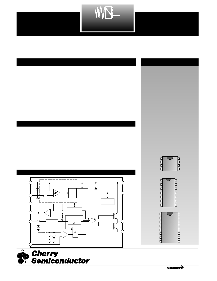
CS2844/3845 SERIES
Current Mode PWM Control Circuit
with 50% Max Duty Cycle
CS2844/CS3844
CS2845/CS3845
Description
Block Diagram
Absolute Maximum Ratings
Supply Voltage (I
CC
<30mA).........................................................................Self Limiting
Supply Voltage (Low Impedance Source) .................................................................30V
Output Current..............................................................................................................�1A
Output Energy (Capacitive Load) ................................................................................5�J
Analog Inputs (V
FB
, V
SENSE
) .........................................................................-0.3V to 5.5V
Error Amp Output Sink Current .............................................................................10mA
Lead Temperature Soldering
Wave Solder (through hole styles only) ...................10 sec. max, 260�C peak
Reflow (SMD styles only) ....................60 sec. max above 183�C, 230�C peak
1
COMP
2
3
4
V
FB
Sense
OSC
V
REF
V
CC
V
OUT
Gnd
8
7
6
5
8 Lead PDIP & SO Narrow
10
7
14
13
12
8
1
2
3
4
5
6
11
9
COMP
NC
V
FB
NC
Sense
NC
OSC
V
REF
NC
V
CC
V
CC
Pwr
V
OUT
Pwr Gnd
Gnd
14 Lead SO Narrow
The CS3844/45 provides all the neces-
sary features to implement off-line
fixed frequency current-mode control
with a minimum number of external
components.
The CS3844 family incorporates a new
precision temperature-controlled oscil-
lator to minimize variations in fre-
quency. An internal toggle flip-flop,
which blanks the output every other
clock cycle, limits the duty-cycle range
to less than 50%. An undervoltage
lockout ensures that V
REF
is stabilized
before the output stage is enabled. In
the CS2844/CS3844 turn on occurs at
16V and turn off at 10V. In the
CS2845/CS3845 turn on is at 8.4V and
turn off at 7.6V.
Other features include low start-up
current, pulse-by-pulse current limit-
ing, and a high-current totem pole out-
put for driving capacitive loads, such
as gate of a power MOSFET. The out-
put is low in the off state, consistent
with N-channel devices.
16
15
14
13
12
11
11
10
9
1
2
3
4
5
6
7
8
NC
NC
COMP
V
FB
SENSE
OSC
NC
NC
NC
V
REF
V
CC
V
CCPwr
V
O
Gnd
Pwr Gnd
NC
16 Lead SO Wide
Cherry Semiconductor Corporation
2000 South County Trail, East Greenwich, RI 02818
Tel: (401)885-3600 Fax: (401)885-5786
Email: info@cherry-semi.com
Web Site: www.cherry-semi.com
A
Company
�
Rev. 3/17/99

2
Electrical Characteristics: -25 T
A
85�C for CS2844/2845, 0 T
A
70�C for CS3844/3845. V
CC
= 15V (Note 1); R
T
= 10k,
C
T
= 3.3nF for sawtooth mode., unless otherwise stated.
CS2844/CS2845
CS3844/CS3845
PARAMETER
TEST CONDITIONS
MIN
TYP
MAX
MIN
TYP
MAX UNITS
CS2844/3845 SERIES
s
Reference Section
Output Voltage
T
J
=25�C, I
REF
=1mA
4.95
5.00
5.05
4.90
5.00
5.10 V
Line Regulation
12V
CC
25V
6
20
6
20
mV
Load Regulation
1I
REF
20mA
6
25
6
25
mV
Temperature Stability
(Note 2)
0.2
0.4
0.2
0.4
mV/�C
Total Output Variation
Line, Load, Temp. (Note 2)
4.90
5.10
4.82
5.18 V
Output Noise Voltage
10Hz f10kHz, T
J
=25�C (Note 2)
50
50
�V
Long Term Stability
T
A
=125�C, 1000 Hrs. (Note 2)
5
25
5
25
mV
Output Short Circuit
T
A
=25�C
-30
-100
-180
-30
-100
-180 mA
s
Oscillator Section
Initial Accuracy
Sawtooth Mode, T
J
=25�C
47
52
57
47
52
57
kHz
Voltage Stability
12V
CC
25V
0.2
1.0
0.2
1.0
%
Temperature Stability
Sawtooth Mode T
MIN
T
A
T
MAX
(Note 2)
5
5
%
Amplitude
V
OSC
(peak to peak)
1.7
1.7
V
s
Error Amp Section
Input Voltage
V
COMP
=2.5V
2.45
2.50
2.55
2.42
2.50
2.58 V
Input Bias Current
V
FB
=0V
-0.3
-1.0
-0.3
-2.0 �A
A
VOL
2V
OUT
4V
65
90
65
90
dB
Unity Gain Bandwidth
(Note 2)
0.7
1.0
0.7
1.0
MHz
PSRR
12V
CC
25V
60
70
60
70
dB
Output Sink Current
V
FB
=2.7V, V
COMP
=1.1V
2
6
2
6
mA
Output Source Current
V
FB
=2.3V, V
COMP
=5V
-0.5
-0.8
-0.5
-0.8
mA
V
OUT
HIGH
V
FB
=2.3V, R
L
=15k to Gnd
5
6
5
6
V
V
OUT
LOW
V
FB
=2.7V, R
L
=15k to V
REF
0.7
1.1
0.7
1.1
V
s
Current Sense Section
Gain
(Notes 3 & 4)
2.85
3.00
3.15
2.85
3.00
3.15 V/V
Maximum Input Signal
V
COMP
=5V (Note 3)
0.9
1.0
1.1
0.9
1.0
1.1
V
PSRR
12V
CC
25V (Note 3)
70
70
dB
Input Bias Current
V
Sense
=0V
-2
-10
-2
-10
�A
Delay to Output
T
J
=25�C (Note 2)
150
300
150
300
ns
s
Output Section
Output Low Level
I
SINK
=20mA
0.1
0.4
0.1
0.4
V
I
SINK
=200mA
1.5
2.2
1.5
2.2
V
Output High Level
I
SOURCE
=20mA
13.0
13.5
13.0
13.5
V
I
SOURCE
=200mA
12.0
13.5
12.0
13.5
V
Rise Time
T
J
=25�C, C
L
=1nF (Note 2)
50
150
50
150
ns
Fall Time
T
J
=25�C, C
L
=1nF (Note 2)
50
150
50
150
ns
3
CS2844/3845 SERIES
CS2844/CS2845
CS3844/CS3845
PARAMETER
TEST CONDITIONS
MIN
TYP
MAX
MIN
TYP
MAX UNITS
CS2844 CS3844
CS2845/CS3845
PARAMETER
TEST CONDITIONS
MIN
TYP
MAX
MIN
TYP
MAX MIN
TYP
MAX UNITS
Notes:
1. Adjust V
cc
above the start threshold before setting at 15V.
3. Parameter measured at trip point of latch with V
FB
=0.
2.These parameters, although guaranteed, are not 100% tested in production.
4. Gain defined as:
A =
; 0 V
Sense
0.8V.
V
COMP
V
Sense
s
Under-Voltage Lockout Section
Start Threshold
15
16
17
14.5
16
17.5
7.8
8.4
9.0
V
Min. Operating After Turn On
9
10
11
8.5
10
11.5
7.0
7.6
8.2
V
Voltage
Package Pin Description
PACKAGE PIN #
PIN SYMBOL
FUNCTION
s
Total Standby Current
Start-Up Current
0.5
1.0
0.5
1.0
mA
Operating Supply Current
V
FB
=V
Sense
=0V R
T
=10k, C
T
=3.3nF
11
17
11
17
mA
V
CC
Zener Voltage
I
CC
=25mA
34
34
V
s
PWM Section
Maximum Duty Cycle
46
48
50
46
48
50
%
Minimum Duty Cycle
0
0
%
8L 14L 16L
PDIP/SO
SO Narrow
SO Wide
1
1
3
COMP
Error amp output, used to compensate error amplifier.
2
3
4
V
FB
Error amp inverting input.
3
5
5
Sense
Noninverting input to Current Sense Comparator.
4
7
6
OSC
Oscillator timing network with Capacitor to Ground, resis-
tor to V
REF
.
5
9
11
Gnd
Ground.
8
10
Pwr Gnd
Output driver Ground.
6
10
12
V
OUT
Output drive pin.
11
13
V
CC
Pwr
Output driver positive supply.
7
12
14
V
CC
Positive power supply.
8
14
15
V
REF
Output of 5V internal reference.
2,4,6,13
1,2,7,8,9,16
NC
No Connection.
Electrical Characteristics: -25T
A
85�C for CS2844/2845, 0T
A
70�C for CS3844/3845. V
CC
=15V (Note 1); R
T
=10k,
C
T
=3.3nF for sawtooth mode., unless otherwise stated.
4
CS2844/3845 SERIES
Undervoltage Lockout
During Undervoltage Lockout (Figure 1), the output driv-
er is biased to sink minor amounts of current. The output
should be shunted to ground with a resistor to prevent
activating the power switch with extraneous leakage cur-
rents.
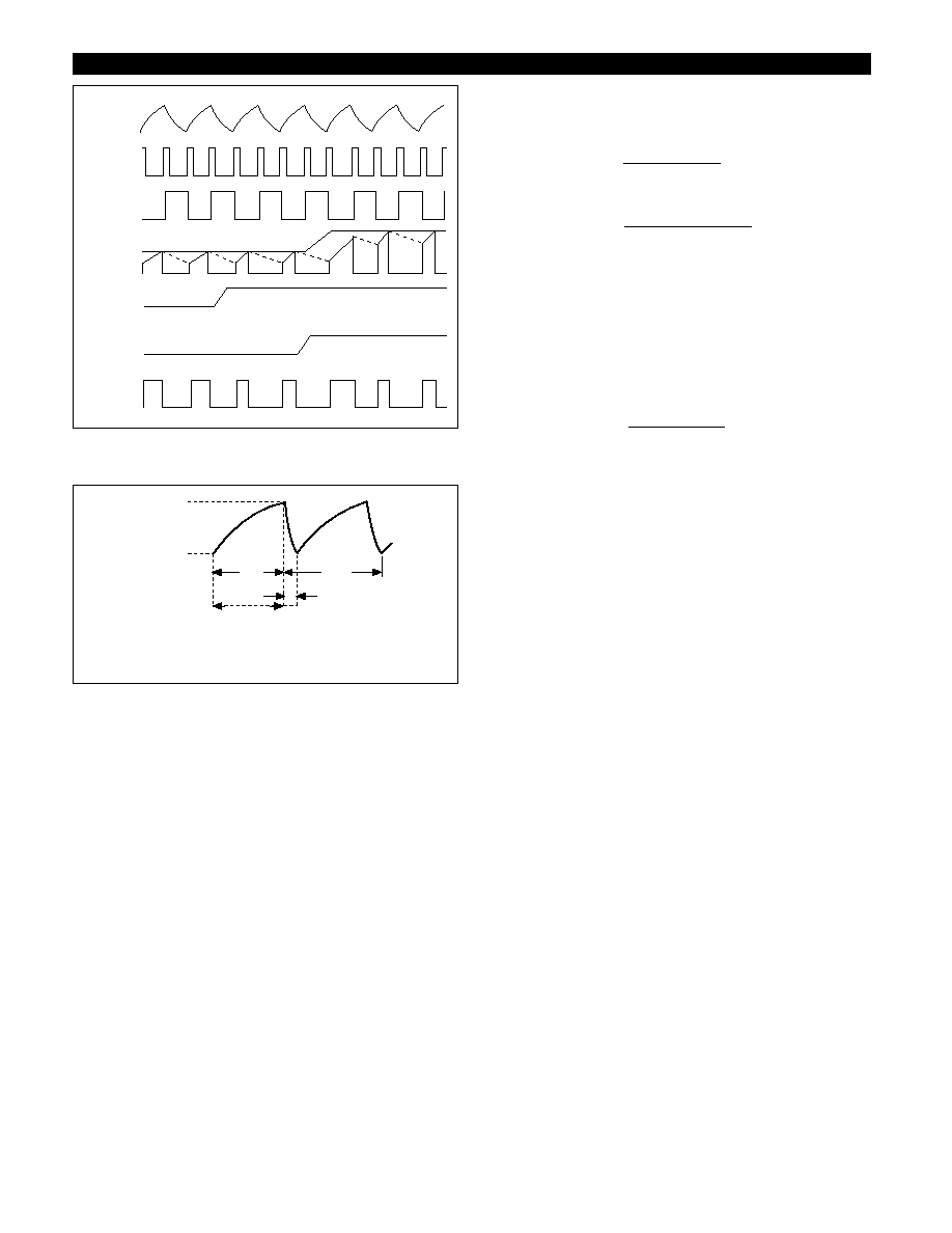
PWM Waveform
To generate the PWM waveform, the control voltage from
the error amplifier is compared to a current sense signal
which represents the peak output inductor current (Figure
2). An increase in V
CC
causes the inductor current slope to
increase, thus reducing the duty cycle. This is an inherent
feed-forward characteristic of current mode control, since
the control voltage does not have to change during
changes of input supply voltage.
When the power supply sees a sudden large output cur-
rent increase, the control voltage will increase allowing
the duty cycle to momentarily increase. Since the duty
cycle tends to exceed the maximum allowed to prevent
transformer saturation in some power supplies, the inter-
nal oscillator waveform provides the maximum duty cycle
clamp as programmed by the selection of OSC compo-
nents.
Circuit Description
Test Circuit Open Loop Laboratory Test Fixture
V
REF
V
CC
V
OUT
1k
1W
0.1
�
F
0.1
�
F
V
REF
V
CC
V
OUT
Gnd
V
FB
Sense
OSC
COMP
5k
100k
4.7k
1k
Error Amp
Adjust
4.7k
Sense
Adjust
R
T
2N2222
C
T
Gnd
A
V
CC
V
ON
16V 8.4V
V
OFF
10V 7.6V
CSX844
CSX845
ON/OFF Command
to reset of IC
<15mA
<1mA
V
ON
V
OFF
I
CC
V
CC
Figure 1: Startup voltage for CSX844 and CSX845.
5
Setting the Oscillator
The times T
c
and T
d
can be determined as follows:
Grounding
High peak currents associated with capacitive loads neces-
sitate careful grounding techniques. Timing and bypass
capacitors should be connected close to Gnd in a single
point ground.
The transistor and 5k potentiometer are used to sample
the oscillator waveform and apply an adjustable ramp to
Sense.
CS2844/3845 SERIES
t
on
t
off
V
upper
V
lower
t
C
t
d
t
on =
t
C
t
off =
t
C+
2t
d
Circuit Description: continued
Substituting in typical values for the parameters in the
above formulas:
V
REF
= 5.0V, V
upper
= 2.7V, V
lower
= 1.0V, I
d
= 8.3mA,
then
t
c
0.5534R
T
C
T
t
d
= R
T
C
T
ln
For better accuracy R
T
should be 10k.
)
2.3 - 0.0083 R
T
4.0 - 0.0083 R
T
(
V
CC
I
O
V
O
Switch
Current
EA Output
Toggle
F/F Output
OSC
RESET
V
OSC
Figure 2: Timing Diagram
Figure 3: Duty Cycle parameters.
t
c
= R
T
C
T
ln
t
d
= R
T
C
T
ln
)
V
REF
- I
d
R
T
- V
lower
V
REF
- I
d
R
T
- V
upper
(
)
V
REF
- V
lower
V
REF
- V
upper
(