1
Features
+
-
+
-
V
REF
SYNC
Oscillator
Error
Amp 1
Error
Amp 2
Latching
PWM 2
Latching
PWM 1
V
REF
Undervoltage
Lockout
5.0V Ref
V
CC
Undervoltage
Lockout
V
CC
V
FB1
COMP
1
ENABLE
2
V
FB2
COMP
2
C
T
R
T
Gnd
Pwr Gnd
Sense
2
V
OUT2
Sense
1
V
OUT
1
s
Oscillator has Precise
Duty Cycle
Limit and Frequency
Control
s
500kHz Current Mode
Operation
s
Automatic Feed Forward
Compensation
s
Separate Latching PWMs
for Cycle-By-Cycle
Current Limiting
s
Internally Trimmed
Reference with
Undervoltage Lockout
s
Switchable Second
Output
s
Two High Current Totem
Pole Outputs
s
Input Undervoltage
Lockout with Hysteresis
s
Low Start-Up and
Operating Current
Package Options
16L PDIP & SO Wide
CS3865C
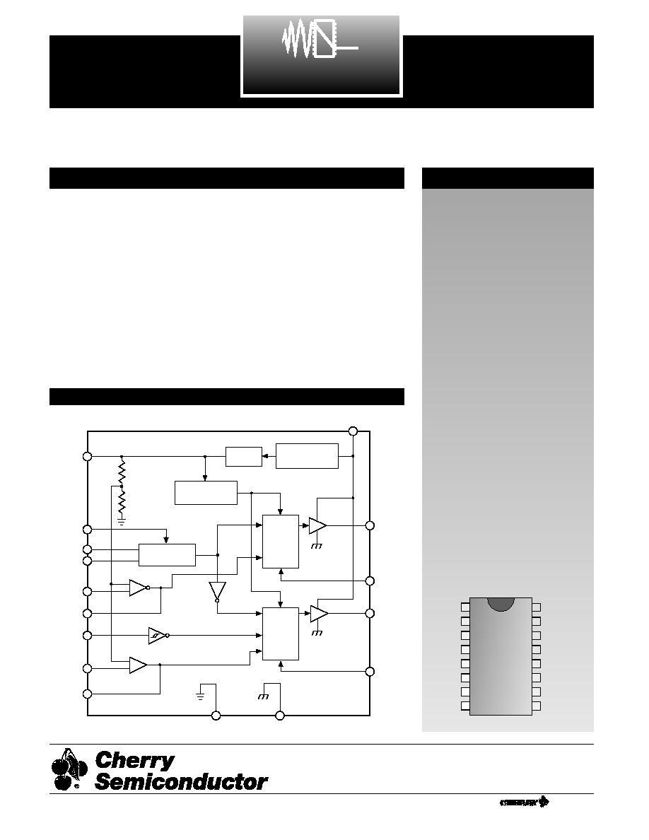
High Performance Dual Channel
Current Mode Controller with ENABLE
1
SYNC
2
3
4
5
6
7
8
C
T
R
T
V
FB1
COMP
1
Sense
1
V
OUT1
Gnd
16
15
14
13
12
11
10
9
V
CC
V
REF
ENABLE
2
V
FB2
COMP
2
Sense
2
V
OUT2
Pwr Gnd
CS3865C
Description
The CS3865C is a high perfor-
mance, fixed frequency, dual cur-
rent mode controller. It is used in
Off-Line and DC to DC converter
applications and require a mini-
mum number of external compo-
nents. This integrated circuit fea-
tures a unique oscillator for precise
duty cycle limit and frequency con-
trol, a temperature compensated
reference, two high gain error
amplifiers, two current sensing
comparators, and two high current
totem pole outputs ideally suited
for driving power MOSFETs. One
of the outputs V
OUT2
is switchable
via the ENABLE
2
pin.
Also included are protective fea-
tures consisting of input and refer-
ence undervoltage lockouts each
with hysteresis, cycle-by-cycle cur-
rent limiting, and a latch for single
pulse metering of each output.
The CS3865C has a 14V start volt-
age and is pin compatible with the
MC34065H.
Block Diagram
Rev. 12/16/96
Cherry Semiconductor Corporation
2000 South County Trail, East Greenwich, RI 02818
Tel: (401)885-3600 Fax: (401)885-5786
Email: info@cherry-semi.com
Web Site: www.cherry-semi.com
A Company
Æ

2
Electrical Characteristics:
V
CC
= 15V, R
T
= 8.2k, C
T
= 3.3nF, for typical values T
A
=25∞C, for min/max values T
A
is the operating
ambient temperature range that applies [Note 3].
PARAMETER
TEST CONDITIONS
MIN
TYP
MAX
UNIT
Absolute Maximum Ratings
Total Power Supply and Zener Current .........................................................................................................................50mA
Output Current, Source or Sink (Note 1)...........................................................................................................................1.0A
Output Energy (capacitive load per cycle) .......................................................................................................................5.0µJ
Current Sense, Enable and Voltage ......................................................................................................................-0.3 to +5.5V
Feedback Inputs
High State (Voltage)..........................................................................................................................................5.5V
Low State (Reverse Current) ......................................................................................................................-5.0mA
Error Amp Output Sink Current......................................................................................................................................10mA
Storage Temperature Range ................................................................................................................................-65 to +150∞C
Operating Junction Temperature...................................................................................................................................+150∞C
Operating Ambient Temperature.............................................................................................................................0 to +70∞C
Lead Temperature Soldering
Wave Solder (through hole styles only) .................................................................................10 sec. max, 260∞C peak
Reflow (SMD styles only) ..................................................................................60 sec. max above 183∞C, 230∞C peak
CS3865C
s
Reference Section
Reference Output Voltage,
I
OUT
=1.0mA, T
J
=25∞C
4.9
5.0
5.1
V
V
REF
Line Regulation
11VV
CC
15V
2.0
20.0
mV
Load Regulation
1.0mAI
OUT
10mA
3.0
25.0
mV
Total Output Variation over
4.85
5.15
V
Line, Load and Temperature
Output Short Circuit Current
30
100
mA
s
Oscillator and PWM Sections
Total Frequency Variation
11VV
CC
15V, T
low
T
A
T
high
46.5
49.0
51.5
kHz
over Line and Temperature
Frequency Change with
11VV
CC
15V
0.2
1.0
%
Voltage
Duty Cycle at each Output
Maximum
46.0
49.5
52.0
%
Sync Input Current
High State V
IN
=2.4V
170
250
µA
Low State V
IN
=0.8V
80
160
s
Error Amplifiers
Voltage Feedback Input
V
OUT
=2.5V
2.42
2.50
2.58
V
Input Bias Current
V
FB
=5.0V
-0.1
-1.0
µA
Open-Loop Voltage Gain
V
OUT
=2.0 to 4.0V
65
100
dB
Unity Gain Bandwidth
T
J
=25∞C (note 6)
0.7
1.0
MHz
Power Supply Rejection Ratio V
CC
=11V to 15V
60
90
dB
Output Current
Source V
OUT
=3.0V, V
FB
=2.3V
-0.45
-1.00
mA
Sink V
OUT
=1.2V, V
FB
=2.7V
2.00
12.00
mA
Output Voltage Swing
High State, R
L
=15k to ground,
V
FB
=2.3V
5.0
6.2
V
Low State, R
L
=15k to V
REF
,
V
FB
= 2.7V
0.8
1.1

3
CS3865C
PARAMETER
TEST CONDITIONS
MIN
TYP
MAX
UNIT
Note 1: Maximum package power dissipation limits must be observed.
Note 3: Adjust V
CC
above the Start-Up threshold before setting to 15V.
Note 4: This parameter is measured at latch trip point with V
FB
=0V.
Note 5: Comparator gain is defined as:
AV =
Note 6: These parameters are guaranteed by design but not 100% tested
in production.
Note 7: Low duty cycle pulse techniques are used during test to main-
tain junction temperature as close to ambient as possible: T
low
=0∞C ;
T
high
=+70∞C
V Compensation
V Current Sense
s
Current Sense Section
Current Sense Input
(Notes 4 and 5)
2.75
3.00
3.25
V/V
Voltage Gain
Maximum Current Sense
(Note 4)
430
480
530
mV
Input Threshold
Input Bias Current
-2.0
-10.0
µA
Propagation Delay
Current Sense Input to Output (Note 6)
150
300
ns
s
Output 2 Enable Pin
Enable Pin Voltage
High State
Output 2 enabled
3.5
V
REF
V
Low State
Output 2 disabled
0.0
1.5
V
Low State Input Current
V
IL
= 0V
100
250
400
µA
s
Drive Outputs
Output Voltage
Low State
I
SINK
=20mA
0.1
0.4
V
I
SINK
=200mA
1.6
2.5
V
High State
I
SOURCE
=20mA
13.0
13.5
V
I
SOURCE
=200mA
12.0
13.4
V
Output Voltage with
V
CC
=6.0V, I
SINK
=1.0mA
0.1
1.1
V
UVLO Activated
Output Voltage Rise Time
C
L
=1.0nF (Note 6)
28
150
ns
Output Voltage Fall Time
C
L
=1.0nF (Note 6)
25
150
ns
s
Undervoltage Lockout Section
Start-Up Threshold
CS3865C
13
14
15
V
Minimum Operating Voltage
9.0
10.0
11.0
V
After Turn-On
Hysteresis
4
V
s
Total Device
Start-Up Current
V
CC
=12V
0.6
1.0
mA
Operating Current
(Note 7)
20
25
mA
Power Supply Zener Voltage I
CC
=30mA
15.5
17.0
19.0
V
Electrical Characteristics:
V
CC
= 15V, R
T
= 8.2k, C
T
= 3.3nF, for typical values T
A
=25∞C, for min/max values T
A
is the operating
ambient temperature range that applies [Note 3].
4
CS3865C
Package Pin Description
PACKAGE PIN #
PIN SYMBOL
FUNCTION
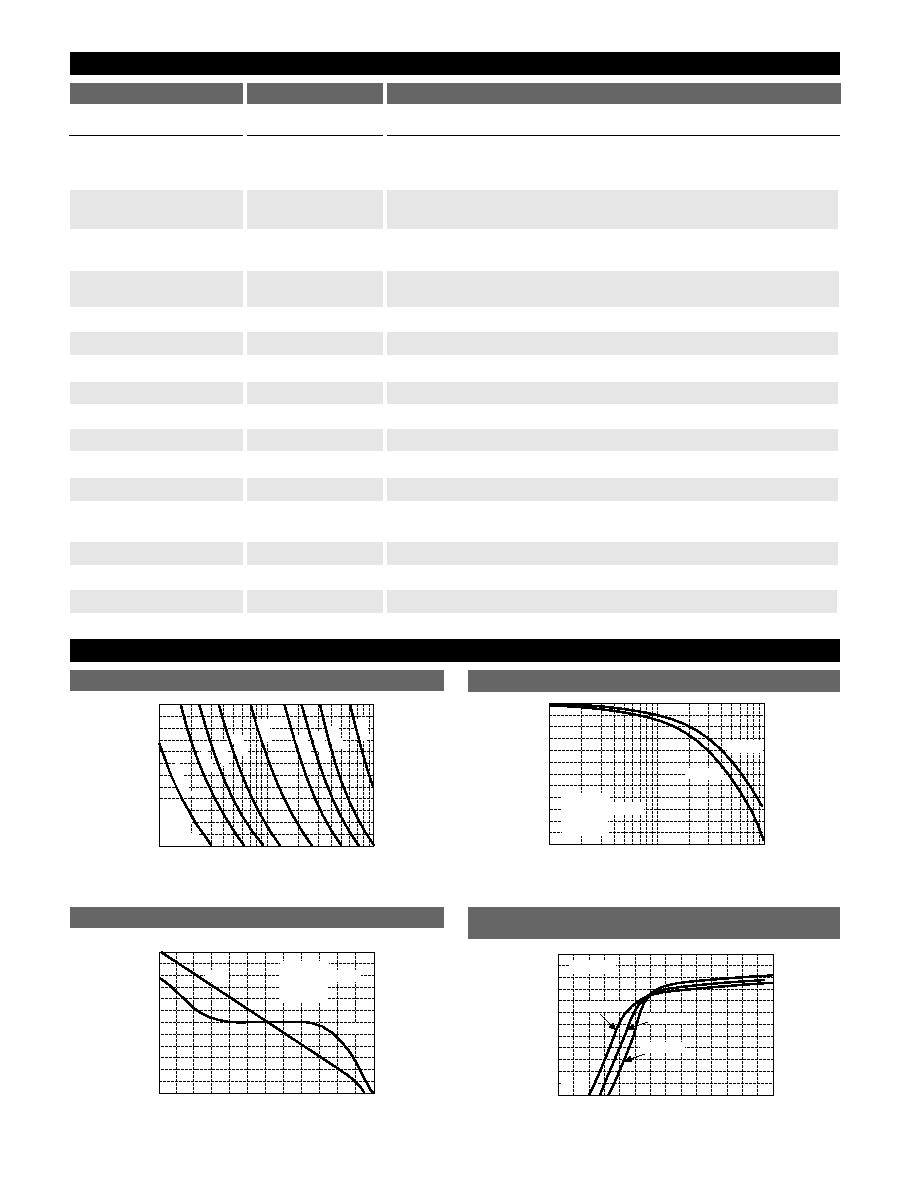
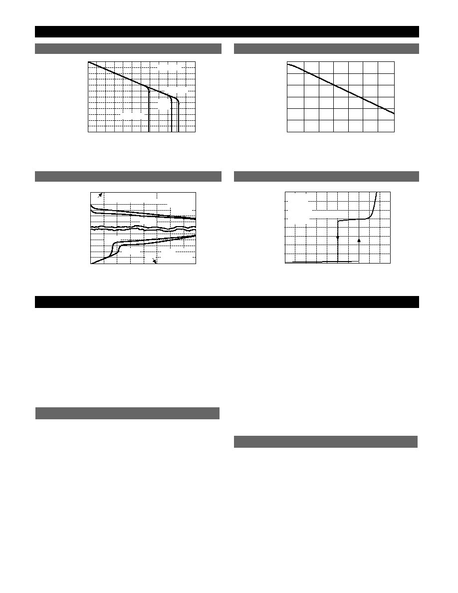
Typical Performance Characteristics
100pF
1.0nF
10k
30k
50k
100k
300k
500k
1.0M
f
OSC
OSCILLATOR FREQUENCY (Hz)
4.0
6.0
8.0
10
12
14
16
R
T
TIMING RESIST
OR (K
)
T
A
=25
∞
C
2.2nF
3.3nF
5.0nF
C
T
=10nF
V
CC
=
15V
220pF
330pF
500pF
10k
30k
50k
100k
300k
500k
1.0M
f
OSC
OSCILLATOR FREQUENCY (Hz)
38
40
42
44
46
48
50
MAXIMUM DUTY
CYCLE (%)
V
CC
= 15V
R
T
= 4.0k
to 16k
C
L
= 15pF
T
A
= 25
∞
C
OUT 2
OUT 1
Max. Output Duty Cycle vs. Oscillator Frequency
Timing Resistor vs. Oscillator Frequency
10k
100k
1.0k
10k
100k
1.0M
10M
f, FREQUENCY (Hz)
-20
0
20
40
60
80
100
A
VOL
, OPEN-LOOP
VOL
T
AGE GAIN (dB)
V
CC
= 15V
V
O
= 1.5V TO 2.5V
R
L
= 100k
T
A
= 25
∞
C
GAIN
PHASE
180
150
120
90
60
30
0
Phase Margin (DEGREES)
0
1.0
2.0
3.0
4.0
5.0
7.0
ERROR AMP OUTPUT VOLTAGE (V)
0
0.1
0.2
0.3
0.4
0.5
0.6
Vth, CURRENT
SENSE
INPUT
THRESHHOLD
(V)
6.0
V
CC
= 15V
T
A
= 125
∞
C
T
A
= 25
∞
C
T
A
= -55
∞
C
Current Sense Input Threshold
vs. Error Amp Output Voltage
Error Amp Open-Loop Gain & Phase vs. Frequency
16 L PDIP & SO Wide
1
SYNC
A positive going pulse applied to this input will synchronize the
oscillator. A DC voltage within the range of 2.4V to 5.5V will inhibit
the oscillator.
2
C
T
Timing capacitor C
T
connects pin to ground setting oscillator fre-
quency.
3
R
T
Resistor R
T
connects to ground setting the charge current for C
T
. Its
value must be between 4.0k and 16k.
4
V
FB1
The inverting input of error amplifier 1. Normally it is connected to
the switching power supply output.
5
COMP
1
The output of error amplifier 1, for loop compensation.
6
Sense
1
Output 1 pulse by pulse current limit.
7
V
OUT1
Drives the power switch at output 1.
8
Gnd
Logic ground
9
Pwr Gnd
Power ground. Power device return is connected to this pin.
10
V
OUT2
Drives the power switch at output 2.
11
Sense
2
Output 2 pulse by pulse current limit.
12
COMP
2
Output of error amplifier 2, for loop compensation.
13
V
FB2
Inverting input of error amplifier 2. Normally it is connected to the
switching power supply output.
14
ENABLE
2
Output 2 disable. A logic low at this pin disables V
OUT2
.
15
V
REF
5.0V reference output. It can source current in excess of 30mA.
16
V
CC
The positive supply of the IC.
5
The CS3865C is a high performance, fixed frequency, dual
channel current mode PWM controller specifically
designed for off-line and DC to DC converter applications.
It offers the designer a cost effective solution with minimal
external components where independent regulation of two
power converters is required. Each channel contains a high
gain error amplifier, current sensing comparator, pulse
width modulator latch, and totem pole output driver. The
oscillator, reference, and undervoltage lockout circuits are
common to both channels.
The oscillator uses precise frequency and duty cycle con-
trol. The frequency is programmed by the values R
T
and
C
T
. Capacitor, C
T
, is charged and discharged by an equal
magnitude internal current source and sink, generating a
symmetrical 50 percent duty cycle waveform at C
T
. The
oscillator peak and valley thresholds are 3.5V and 1.6V
respectively. The source/sink current magnitude is con-
trolled by resistor R
T
. For proper operation over tempera-
ture range, its value should be between 4.0k and 16k.
As C
T
charges and discharges, an internal blanking pulse
is generated that alternately drives the inputs of the upper
and lower NOR gates high. This, in conjunction with a
precise amount of delay time introduced into each chan-
nel, produces well defined non-overlapping output duty
cycles. The second output, V
OUT2
is enabled while C
T
is
charging, and the primary is enabled during the discharge.
Even at 500kHz, each output is capable of approximately
44% duty cycle, making this controller suitable for high
frequency power conversion applications.
In many noise sensitive applications, it may be necessary
to synchronize the converter with an external system
clock. This can be accomplished by applying an external
clock signal. For reliable synchronization, the oscillator fre-
quency should be set about 10% slower than the clock fre-
quency. The rising edge of the clock signal applied to
SYNC, terminates C
T
`s charging and V
OUT2
`s conduction.
By tailoring the clock waveform symmetry, accurate duty
cycle clamping of either output can be achieved.
Each channel contains a fully-compensated error amplifi-
er. The output and inverting input nodes are accessible.
The amplifier features a typical dc voltage gain of 100 dB,
and a unity gain bandwidth of 1.0 MHz with 71 degrees of
phase margin. The non-inverting input is internally biased
at 2.5V. The converter output voltage is typically divided
down and monitored by the inverting input through a
resistor divider. The maximum input bias current is -1.0µA
which will cause an output voltage error that is equal to
the product of the input bias current and the equivalent
input divider resistance.
Error Amplifier
Oscillator
Operating Description
CS3865C
Typical Performance Characteristics: continued
0
20
40
60
80
100
120
I
ref
, REFERENCE SOURCE CURRENT (mA)
-24
-20
-16
-12
-8.0
-4.0
0
V
REF
, REFERENCE
V
oltage (mV)
V
CC
= 15V
T
A
= ≠55
∞
C
T
A
= 125
∞
C
T
A
=
25
∞
C
-55
-25
0
25
50
75
100
125
T
A
, AMBIENT TEMPERATURE (
∞
C)
I
SC
, REFERENCE
SHOR
T
CIRCUIT
CURRENT
(mA)
120
100
80
60
Reference Short Circuit Current vs. Temperature
Reference Voltage Change vs. Source Current
SOURCE SATURATION
(LOAD TO GROUND)
V
CC
=15V
80
µ
S PULSED LOAD
120Hz RATE
T
A
=25
∞
C
T
A
= ≠55
∞
C
T
A
= ≠55
∞
C
T
A
=25
∞
C
SINK
SATURATION
(LOAD TO V
CC
)
GND
0
200
400
600
800
OUTPUT LOAD CURRENT (mA)
V
sat
, OUTPUT
SA
TURA
TION VOL
T
AGE (V)
V
CC
0
-1.0
-2.0
2.0
1.0
0
0
4.0
8.0
12
16
20
V
CC,
SUPPLY VOLTAGE (V)
0
8.0
16
24
32
R
T
=8.2k
C
T
=3.3nF
V
FB
1.2=0V
CURRENT SENSE 1.2=0V
T
A
=25
∞
C
I
CC,
SUPPL
Y
CURRENT
(mA)
Supply Current vs. Supply Voltage CS3865C
Output Saturation Voltage vs. Load Current