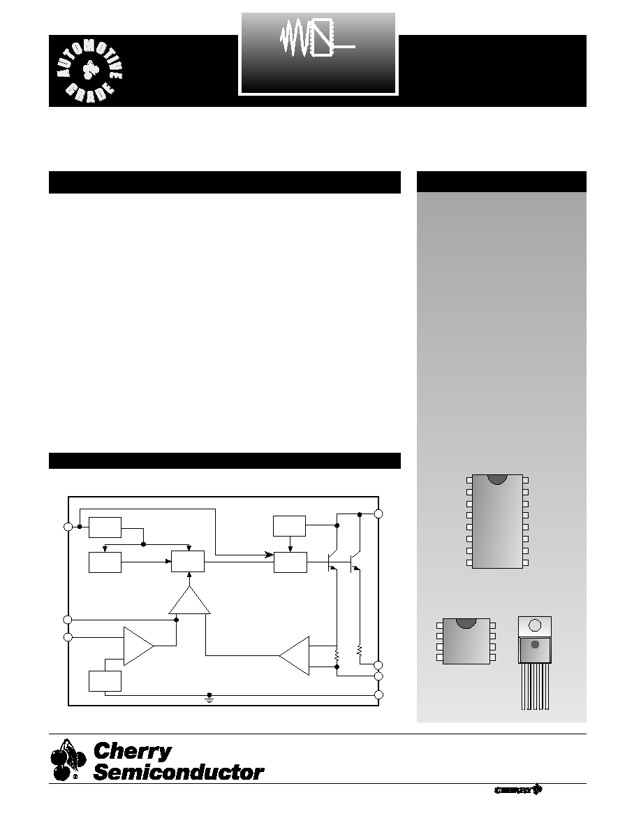
1
Output
Protection
Driver
2.3V
Reg
Logic
40kHz
OSC
Error
Amp
-
+
1.24V
Ref
Current
Amp
-
+
VSW
VC
VIN
VFB
0.22
0.22
COMP
E1*
E2*
Gnd
*Always connect E1 to Ground Pin on DIP package. Both emitters are tied to ground on TO-220 Package.
1.25A,
75V
Switch
-
+
CS3972
1.25A High Efficiency Switching Regulator
CS3972
Description
Block Diagram
Features
s
75V
MAX
, 2A
PEAK
Internal
Switch
s
3V to 60V Input Voltage
Range
s
6mA Input Supply
Current
s
1.24V Precision Reference
s
40kHz Switching
Frequency
s
Variable Current Limit
with External Voltage
Clamp
s
Under-Voltage Protection
s
Over-Temperature
Protection
s
External Synchronization
Package Options
5L TO-220
Tab (Gnd)
8L PDIP
1
Gnd
V
C
V
FB
NC
E
2
V
SW
E
1
V
IN
1
1 V
C
2 V
FB
3 Gnd
4 V
SW
5 V
IN
16L SO Wide
1
Gnd
NC
NC
NC
NC
V
IN
E
1
V
SW
E
2
V
C
V
FB
NC
NC
NC
NC
NC
The CS3972 is a 1.25A, 60V, current
mode, high efficiency, switching
regulator circuit. It can be config-
ured in buck, boost, forward, iso-
lated and non-isolated topologies,
using a single-ended switch.
The IC contains a 1.25A high effi-
ciency output switch, precision
bandgap reference, voltage regula-
tor, error amplifier, oscillator, con-
trol, and protection circuitry.
Output transistor efficiency is
achieved by keeping the switch in
quasi-saturation when it is on. This
minimizes the switch turn-off
delay time and power dissipation,
an important consideration for
applications with wide ranging
loads.
The precision reference is internally
trimmed to 1.24V, while the oscilla-
tor frequency is internally trimmed
to 40kHz. The on board 2.3V regu-
lator powers the internal circuitry.
By keeping the voltage regulator at
2.3V, the IC is able to operate down
to 3V and maintain a constant input
supply current of 6mA(typ).
Synchronization mode is achieved
by applying a pulsating V
C
voltage
of less than 0.2V with a duration of
about 0.5�s to V
C
pin. The switch-
ing frequency can be adjusted from
50kHz to 70kHz. The IC's synchro-
nization mode is set externally.
Protection circuitry includes a vari-
able current limit with external
voltage clamp, under-voltage and
over-temperature protection.
Rev. 6/23/99
Cherry Semiconductor Corporation
2000 South County Trail, East Greenwich, RI 02818
Tel: (401)885-3600 Fax: (401)885-5786
Email: info@cherry-semi.com
Web Site: www.cherry-semi.com
A Company
�
2
Absolute Maximum Ratings
CS3972
PARAMETER
TEST CONDITIONS
MIN
TYP
MAX
UNIT
Input Voltage Range ........................................................................................................................................................3V to 60V
Output Switching Voltage.........................................................................................................................................................75V
Voltage Transient (t
r
=10�s, t
f
=400ms) ......................................................................................................................................60V
ESD (Human Body Model; R=1.5k, C=100pF) ...................................................................................................................2kV
Junction Temperature Range...............................................................................................................................-40�C to +150�C
Storage Temperature Range ................................................................................................................................-65�C to +150�C
Lead Temperature Soldering
Wave Solder (through hole styles only)......................................................................................10 sec. max, 260�C peak
Reflow (SMD styles only) ......................................................................................60 sec. max above 183�C, 230�C peak
Feedback Pin Voltage (1ms transient)...................................................................................................................................�15V
Electrical Characteristics:
For 3VV
CC
60V, -40�CT
A
125�C unless otherwise specified.
s
Reference Voltage
V
C
=0.8V; V
FB
=V
REF
1.214
1.244
1.274
V
Line Regulation
V
C
=0.8V; V
FB
=V
REF
, 3VV
IN
60V
0.03
%/V
Feedback Input Current
V
C
=0.8V; V
FB
=V
REF
350
1100
nA
Minimum Input Voltage
V
C
=V
FB
=V
REF
2.6
3.0
V
Supply Current
V
C
=0.6V; 3VV
IN
60V
6.0
9.0
mA
Supply Current Increase
during switch on time
V
C
=open, 1.0VV
FB
1.5V
25
mA/A
Switching Frequency
V
C
=V
FB
=V
REF;
V
SW
=15V 33
40
47
kHz
Maximum Duty Cycle
V
C
=2V; V
FB
=open, V
SW
=15V
92
%
V
C
Threshold
V
FB
=open; V
SW
=15V, 0.60
0.90
1.25
V
duty cycle=0%
s
Error Amplifier
Transconductance
V
C
=0.8V; V
FB
=V
REF
, I
C
=�25�A
2400
4400
7000
�mho
Source/Sink Current
V
C
=1.5V 120
200
400
�A
High Voltage Clamp
V
FB
=1.0V
2.0
V
Low Voltage Clamp
V
FB
=1.5V
0.38
V
Gain
0.9VV
C
1.4V, V
FB
=V
REF
800
V/V
s
Output Switch
Breakdown Voltage
V
C
=0.5V; 3VV
IN
60V, I
OUT
=5mA 75
90
V
On Resistance
V
C
=open, V
FB
=0.8V, I
OUT
=1.25A 0.6
1.0
Control Voltage to Switch
1.2VV
C
1.8V
2
A/V
Current Transconductance
Current Limit
Duty Cycle50%, T
J
25�C 1.25
3.00
A
Duty Cycle50%, T
J
<25�C 1.25
3.50
A
Duty Cycle=80%
1.00
2.50
A
Duty Cycle=80% (Note 1)
0.50
2.50
A
Note 1: 16 lead SO wide package only.
3
Package Pin Description
PACKAGE PIN #
PIN SYMBOL
FUNCTION
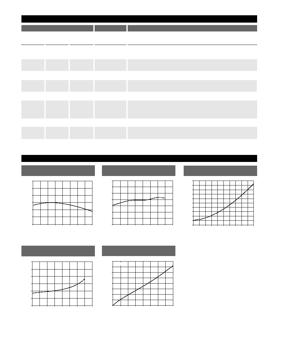
Typical Performance Characteristics
1.274
1.264
1.254
1.244
1.234
1.224
1.214
-50
-25
-0
25
50
75
100
125
150
Temperature (
�
C)
Reference V
oltage (V)
Reference Voltage vs. Temperature
47
45
43
41
39
37
33
-50
-25
-0
25
50
75
100
125
150
Temperature (
�
C)
Frequency (kHz)
35
Switching Frequency vs. Temperature
100
90
80
70
60
50
0
0
0.2
0.4
0.6
0.8
1.0
1.2
1.4
1.6
Switch Current (A)
Driver Current (mA)
10
40
30
20
1.8
2.0
Driver Current vs. Switch Current
97
96
95
93
92
91
90
-50
-25
-0
25
50
75
100
125
150
Junction Temperature (
�
C)
Duty Cycle (%)
Maximum Duty Cycle
1.6
1.4
1.2
1.0
0.8
0.6
0
0
0.50
1.00
1.25
1.75
Switch Current (A)
Switch Saturation V
oltage (V)
0.4
0.2
2.0
0.25
0.75
1.50
T
j
=25
�
C
Switch Saturation Voltage
16L
5L
8L
SO Wide
TO-220
PDIP
16
3
1
Gnd
Logic and power ground on TO-220. Logic ground only on 8L
PDIP.
2
1
2
V
C
Control voltage can be used for frequency compensation, cur-
rent limit threshold, frequency synchronization, and soft start.
3
2
3
V
FB
Feedback voltage is the negative input to the error amplifier.
1,4,5,6,7,8,
4
NC
No connection.
10,12,15
9
5
5
V
IN
Supply input voltage with a range of 3V to 60V.
11
6
E
1
Emitter One is a power ground which should always be con-
nected to logic ground since it is used as the negative input to
the current sense amp.
13
4
7
V
SW
Collector of internal 75V NPN power switch.
14
8
E
2
Emitter Two is a power ground which can be left disconnected
to reduce the switch rating to 625mA.
CS3972
The CS3972 has an on board, high current NPN transistor
in its output stage. The output transistor is switched on
every 25�s by the on board 40 kHz oscillator. The output
is switched off as soon as the output current reaches a
dynamically controlled level. That level is determined by
three factors: the current drawn by the load, the input
voltage, and the output voltage. This control scheme has
several benefits. The IC reacts quickly to overvoltage and
short circuit conditions and it is less sensitive to input
voltage fluctuation.
Current drawn by the load influences when the output
stage turns off. The voltage across the internal high preci-
sion resistor (0.11) in the emitter of the output transistor
generating the input to the current sensing amplifier. The
output of the current sensing amplifier provides one of the
inputs to the comparator.
The other input to the comparator connected to the out-
put of the error amplifier whose inverting input is con-
nected to the output voltage through the feedback circuit-
ry while its noninverting input is set to an internal refer-
ence voltage of 1.24V. When the current sensing amplifier
output exceeds the error amplifier output, the comparator
switches off, triggering the logic which turns off the out-
put stage.
All on board amplifier, logic and protection circuitry uses
the internal 2.3V reference to minimize quiescent current
drain (6mA) and permits IC operation down to 3V.
The anti-saturation circuitry minimizes output switch
turn off time and power dissipation, by keeping the
power NPN at the edge of saturation.
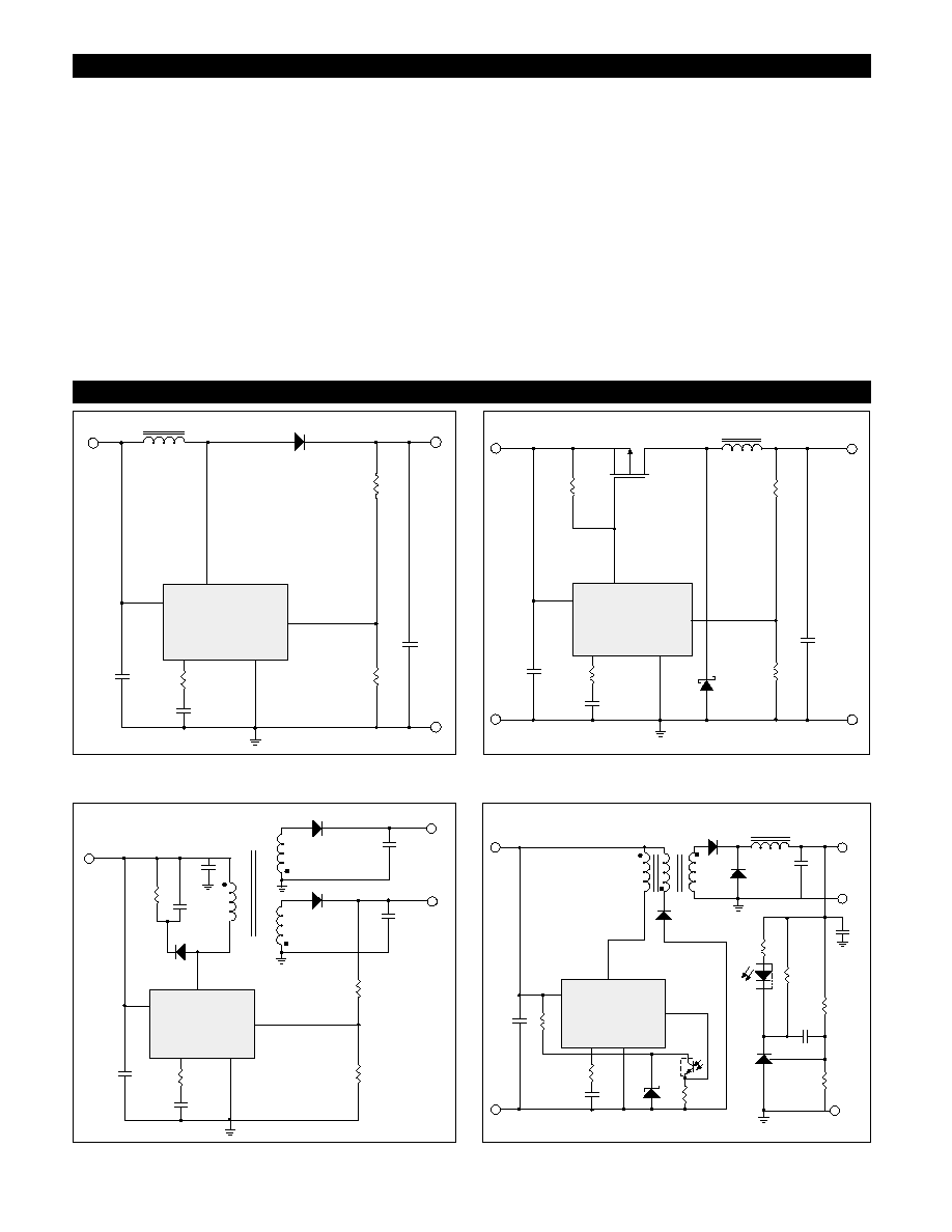
4
Circuit Description
Application Diagrams
V
IN
D1
C
1
+
R
1
C
2
R
3
C
3
(1.24V)
R
2
V
OUT
V
IN
V
C
Gnd
V
FB
V
SW
CS3972
L1
+
V
IN
Q1
R
1
C
1
+
R
2
C
2
D
1
R
4
C
3
(1.24V)
R
3
V
OUT
V
IN
V
C
Gnd
V
FB
V
SW
CS3972
L1
+
V
IN
TR1
R
1
C
2
+
R
2
C
3
R
5
(1.24V)
R
4
V
OUT1
V
IN
V
C
Gnd
V
FB
V
SW
CS3972
C
4
C
1
C
5
+
C
6
+
V
OUT2
+V
IN
TR1
C
2
+
R
2
C
3
R
7
R
5
V
OUT
V
IN
V
C
Gnd
V
FB
V
SW
CS3972
C
3
+
C
5
L
1
D
2
D
1
R
4
1/2
OC1
R
6
C
4
U
1
R
3
D
1
R
1
�V
IN
D
3
1/2
OC1
Figure 1: Boost Regulator
Figure 2: Buck Regulator with the External Switch
Figure 3: Flyback Multiple Output Regulator
Figure 4: Isolated Forward Regulator
CS3972

Thermal Data
5L
8L
16L
TO-220
PDIP
SO Wide
R
JC
typ
1.7
52
23
�C/W
R
JA
typ
50
100
105
�C/W
D
Lead Count
Metric
English
Max
Min
Max
Min
8 Lead PDIP
10.16
9.02
.400
.355
16 Lead SO Wide
10.50
10.10
.413
.398
5
CS3972
Package Specification
PACKAGE DIMENSIONS IN mm (INCHES)
PACKAGE THERMAL DATA
Plastic DIP (N); 300 mil wide
0.39 (.015)
MIN.
2.54 (.100) BSC
1.77 (.070)
1.14 (.045)
D
Some 8 and 16 lead
packages may have
1/2 lead at the end
of the package.
All specs are the same.
.203 (.008)
.356 (.014)
REF: JEDEC MS-001
3.68 (.145)
2.92 (.115)
8.26 (.325)
7.62 (.300)
7.11 (.280)
6.10 (.240)
.356 (.014)
.558 (.022)
Surface Mount Wide Body (DW); 300 mil wide
1.27 (.050) BSC
7.60 (.299)
7.40 (.291)
10.65 (.419)
10.00 (.394)
D
0.32 (.013)
0.23 (.009)
1.27 (.050)
0.40 (.016)
REF: JEDEC MS-013
2.49 (.098)
2.24 (.088)
0.51 (.020)
0.33 (.013)
2.65 (.104)
2.35 (.093)
0.30 (.012)
0.10 (.004)

6
Package Specification
Ordering Information
Rev. 6/23/99
CS3972
Part Number
Description
CS3972YN8
8L PDIP
CS3972YDW16
16L SO Wide
CS3972YDWR16
16L SO Wide (tape & reel)
CS3972YT5
TO-220 Straight
CS3972YTVA5
TO-220 Vertical
CS3972YTHA5
TO-220 Horizontal
� 1999 Cherry Semiconductor Corporation
Cherry Semiconductor Corporation reserves the
right to make changes to the specifications without
notice. Please contact Cherry Semiconductor
Corporation for the latest available information.
5 Lead TO-220 (T) Straight
2.87 (.113)
2.62 (.103)
6.93(.273)
6.68(.263)
9.78 (.385)
10.54 (.415)
1.02(.040)
0.63(.025)
1.83(.072)
1.57(.062)
0.56 (.022)
0.36 (.014)
2.92 (.115)
2.29 (.090)
1.40 (.055)
1.14 (.045)
4.83 (.190)
4.06 (.160)
6.55 (.258)
5.94 (.234)
14.22 (.560)
13.72 (.540)
1.02 (.040)
0.76 (.030)
3.71 (.146)
3.96 (.156)
14.99 (.590)
14.22 (.560)
5 Lead TO-220 (TVA) Vertical
1.68
(.066) typ
1.70 (.067)
7.51 (.296)
1.78 (.070)
4.34 (.171)
0.56 (.022)
0.36 (.014)
1.40 (.055)
1.14 (.045)
4.83 (.190)
4.06 (.160)
14.99 (.590)
14.22 (.560)
2.92 (.115)
2.29 (.090)
.94 (.037)
.69 (.027)
8.64 (.340)
7.87 (.310)
6.80 (.268)
10.54 (.415)
9.78 (.385)
2.87 (.113)
2.62 (.103)
6.55 (.258)
5.94 (.234)
3.96 (.156)
3.71 (.146)
5 Lead TO-220 (THA) Horizontal
0.81(.032)
1.70 (.067)
6.81(.268)
1.40 (.055)
1.14 (.045)
5.84 (.230)
6.60 (.260)
6.83 (.269)
0.56 (.022)
0.36 (.014)
10.54 (.415)
9.78 (.385)
6.55 (.258)
5.94 (.234)
3.96 (.156)
3.71 (.146)
1.68
(.066)
TYP
14.99 (.590)
14.22 (.560)
2.77 (.109)
2.29 (.090)
2.92 (.115)
4.83 (.190)
4.06 (.160)
2.87 (.113)
2.62 (.103)