 | –≠–ª–µ–∫—Ç—Ä–æ–Ω–Ω—ã–π –∫–æ–º–ø–æ–Ω–µ–Ω—Ç: CS4161XN8 | –°–∫–∞—á–∞—Ç—å:  PDF PDF  ZIP ZIP |
1
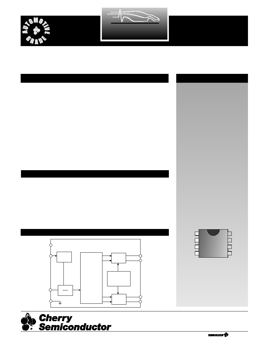
Features
COILB-
SENSOR
SELECT
Coil
Driver
B
Coil
Driver
A
Overvoltage
and Short
Circuit
Protection
Sequencer
COILB
+
COILA-
COILA+
Input
Comp.
∏ 1
Gnd
V
CC
∏ 2
s
Undervoltage Lockout
s
Cross-conduction
Prevention Logic
s
Divide by 1 and Divide
by 2 Modes
s
Guaranteed Monotonic
s
On Chip Flyback Diodes
s
Fault Protection
Overvoltage
Load Dump Protection
to 60V
Package Option
8 Lead PDIP
CS4161
85mA Dual H-Bridge Odometer Driver
with Divide by Select and UVLO
1
Gnd
COILA+
COILA–
SENSOR
V
CC
COILB+
COILB–
SELECT
CS4161
Description
The CS4161 is a Stepper Motor
Driver that implements an H-Bridge
design in order to drive two coils in
an eight step sequence per revolu-
tion in the divide by 1 mode; 16 step
sequence in the divide by 2 mode.
The H-Bridge is capable of deliver-
ing 85mA to the load.
The sequencer insures that the
odometer is monotonic. This
sequencer is configured such that
simultaneous conduction does not
occur. Before each successive out-
put sequence the part is taken
through a state where both outputs
are turned off individually. This
tends to minimize the inductive
kick back energy that the part must
absorb. On chip clamp diodes are
across each output to protect the
part from the kick back energy that
it must absorb.
The CS4161 includes overvoltage
and short circuit protection circuit-
ry. It is lead for lead compatible
with the CS-8441. The CS4161
includes an additional undervoltage
lockout (UVLO) function which dis-
ables the output stage until the sup-
ply voltage rises above 5.6V, typi-
cally. The UVLO has hysteresis to
prevent any power up glitching.
Block Diagram
Absolute Maximum Ratings
Supply Voltage (V
CC
) (continuous) -40˚C to +105˚C .......................-0.5 to 24V
(100ms pulse transient) -40˚C to +105˚C...........................-0.5 to 60V
Input Voltage (V
IN
) ...................................................................-0.3 to V
CC
+0.3V
Operating Temperature Range ....................................................-40°C to 105°C
Storage Temperature Range (TSTG) ...........................................-65°C to 150°C
Junction Temperature Range .......................................................-40°C to 150°C
ESD (Human Body Model) .............................................................................2kV
Lead Temperature Soldering
Wave Solder (through hole styles only)............10 sec. max, 260°C peak
Cherry Semiconductor Corporation
2000 South County Trail, East Greenwich, RI 02818
Tel: (401)885-3600 Fax: (401)885-5786
Email: info@cherry-semi.com
Web Site: www.cherry-semi.com
A Company
®
Rev. 1/28/97
2
Electrical Characteristics: Unless otherwise stated, these specifications apply for -40°C ≤ T
A
≤ 105°C, 6.5V ≤ V
CC
≤ 15.5V.
All voltage shall be referenced to Gnd unless otherwise noted. Overvoltage shutdown of coils occurs when V
CC
> 16V.
PARAMETER
TEST CONDITIONS
MIN
TYP
MAX
UNIT
CS4161
Package Lead Description
PACKAGE LEAD #
LEAD SYMBOL
FUNCTION
8L PDIP
1
Gnd
Ground connection.
2
COILA+
Output stage, when active, this lead supplies current to COIL A.
3
COILA-
Output stage, when active, this lead supplies current to COIL A.
4
SENSOR
Input signal from wheel speed or engine rpm.
5
SELECT
Selects divide by 1 or divide by 2 mode.
6
COILB-
Output stage, when active, this lead supplies current to COIL B.
7
COILB+
Output stage, when active, this lead supplies current to COIL B.
8
V
CC
Supply Voltage.
s Supply, V
CC
Supply Voltage Range
-40°C ≤ TA ≤ 105°C
6.5
15.5
V
DC
-40°C ≤ TA ≤ 25°C
6.5
24.0
V
DC
Transient Pulse, 100ms
35.0
V
DC
Supply Current
V
CC
= 15.5 V
DC
, Outputs not loaded
24
35
mA
Overvoltage Shutdown
16
23
V
Undervoltage Lockout Voltage
V
CC
Initial Power up
5.1
5.6
6.1
V
UVLO Hysteresis
200
600
1000
mV
s Speed Sensor Input, SENSOR
Input Frequency Range
0.2
1.0
kHz
Switching Threshold
1.2
2.6
V
DC
Hysteresis
300
500
mV
DC
Input Bias Current
0.8V
DC
≤ V
IN
≤ V
CC
0.1
±1.0
µA
Input Voltage Range
0
V
CC
V
DC
Operating Input Voltage
10kΩ Resistor in Series
-15 to V
CC
V
DC
Input Clamp Current
I Clamp at V
IN
= 0V
DC
-0.4
-5.0
mA
s Divider Select Input, SELECT
Logic 0 Input Voltage
100
mV
DC
Logic 1 Input Voltage
3.0
V
DC
Logic 0 Input Current
0V ≤ V
IN
≤ 100mV
-1
-100
µA
Logic 1 Input Current
3V ≤ V
IN
≤ 15.5 V
DC
0.75
2.00
mA
s Coil Output Drivers
Coil Load
+25°C
198
210
222
Ω
Coil Inductance
80
mH
Coil Resistance Temperature
Coefficient
0.35
%/°C
* Energized Coil Voltage
V
CC
= 6.5 V
DC
V
CC
- 1.5V V
CC
- 0.9V
V
DC
(Both Polarities) A and B
V
CC
= 10.0 V
DC
V
CC
- 1.6V V
CC
- 1.0V
V
DC
V
CC
= 15.5 V
DC
, -20°C ≤ T
A
≤ 105°C V
CC
- 1.75V V
CC
- 1.1V
V
DC
V
CC
= 15.5 V
DC
, -40°C ≤ T
A
≤ -20°C
V
CC
- 2.0V V
CC
- 1.2V
V
DC
De-energized Coil Leakage Current
±100
µA
s Short Circuit Protection
Short Circuit Threshold
275
400
mA
I Coil A + I Coil B
Short Circuit Turn-Off Delay
5
µs
* Voltage across the coils shall be measured at the specific voltages, but shall also be within linearly interpolated limits.

SENSOR is a PNP comparator input which accepts either a sine
wave or a square wave input. This input is protected from excur-
sions above V
CC
as well as any below ground as long as the cur-
rent is limited to 1.5mA. It has an active clamp set to zero volts to
prevent negative input voltages from disrupting normal opera-
tion. The sensor input can withstand 150V
DC
as long as the input
current is limited to 1.5mA max. using a series resistor of 100kΩ.
Simultaneously energizing the source and sink on either leg is
not permitted, i.e. Q1 & Q2 or Q3 & Q4 cannot be energized
simultaneously.
Circuit function is not affected by inductive transients due to coil
loads as specified in the Transition States section.
The transition states occur as indicated in Table 1 without any
intermediate states permitted.
Table 1: Transition States
The polarity definition for the coil driver outputs is as follows:
Connect
Connect
Polarity
Coil +
Coil -
Positive (+)
V
CC
Gnd
Negative (-)
Gnd
V
CC
The speed sensor input frequency is either divided by one or divid-
ed by two depending on the state of the SELECT input as follows:
Logic 0 = divide by 2
Logic 1 = divide by 1
Divider Select Input
Output State Table
State
Coil A
Coil B
0
+
+
1
OFF
+
2
-
+
3
-
OFF
4
-
-
5
OFF
-
6
+
-
7
+
OFF
Coil Driver Outputs
Speed Sensor Input
3
CS4161
Circuit Operation
Short
Circuit
V
CC
Sense
Resistor
Coil
Short
Circuit
Sense
Resistor
Gnd
Q3
Q4
Q1
Q2
Overvoltage
and
Short
Circuit
Protection
Figure 1: Coil Driver Output
Figure 3: Divide by 2 SELECT Mode
DIVIDE BY TWO MODE SELECT = Gnd
COILA+
COILA–
COILB+
COILB–
V
CC
SELECT
Gnd
SENSOR
CS4161
IGN
D1
R1
R3
Z1
C1
C2
R2
C3
Buffered Speed Signal
(Open Collector Drive)
COIL A
COIL B
Odometer Application Diagram
C1 - 10µF
C2 - 0.1µF
C3 - 0.01µF
R1 - 3.9Ω, 500mW
R2 - 100kΩ
R3 - 15kΩ
D1 - 1A, 600PIV
Z1 - 50V, 500mW
COIL A - 210 ±12Ω, 80mH
COIL B - 210 ±12Ω, 80mH
Figure 2: Divide by 1 SELECT Mode
Part Number
Description
CS4161XN8
8L PDIP
Thermal Data
8L PDIP
R
QJC
typ
52
˚C/W
R
QJA
typ
100
˚C/W
4
CS4161
D
Lead Count
Metric
English
Max
Min
Max
Min
8L PDIP
10.16
9.02
.400
.355
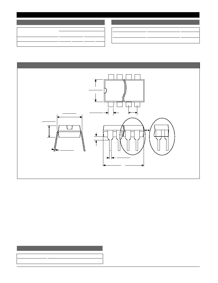
Package Specification
PACKAGE DIMENSIONS IN mm (INCHES)
Ordering Information
PACKAGE THERMAL DATA
Rev. 1/28/97
© 1999 Cherry Semiconductor Corporation
Cherry Semiconductor Corporation reserves the
right to make changes to the specifications without
notice. Please contact Cherry Semiconductor
Corporation for the latest available information.
Plastic DIP (N); 300 mil wide
0.39 (.015)
MIN.
2.54 (.100) BSC
1.77 (.070)
1.14 (.045)
D
Some 8 and 16 lead
packages may have
1/2 lead at the end
of the package.
All specs are the same.
.203 (.008)
.356 (.014)
REF: JEDEC MS-001
3.68 (.145)
2.92 (.115)
8.26 (.325)
7.62 (.300)
7.11 (.280)
6.10 (.240)
.356 (.014)
.558 (.022)