
1
Features
CS452/453
V
BAT
4.5V to 24V
(60V Transient)
I
OUT
Injector
40V
Z
(max)
OUT
V
CC
300
W
Gnd
V
IN
CONTROL
1k
W
19k
W
V
IN
s
Microprocessor
Compatible Inputs
s
On-Chip Power Device
2.4A Peak, Typical CS-452
4.4A Peak, Typical CS453
s
Low Thermal Resistance
To Grounded Tab
s
60V Peak Transient
Voltage
s
Low Saturation Voltage
s
Operates Over a 4.5V to
24V Battery Range
Package Options
5 Lead TO-220
Tab (Gnd)
1
CS452/453
2.4A/4.4A Injector Solenoid Driver
CS452/453
Description
The CS452/453 is a monolithic inte-
grated circuit designed for medium
current solenoid driver applica-
tions. Its typical function is to sup-
ply full battery voltage to fuel injec-
tor(s) for rapid current rise, in order
to produce positive injector open-
ing.
When load current reaches a preset
level (2.4A for CS452, or 4.4A for
CS453), the injector driver reduces
the load current by a 4:1 ratio and
operates as a constant current
source. This condition holds the
injector open and reduces system
power dissipation.
Other solenoid or relay applications
can be equally well served by the
CS452/453. Two high impedance
inputs are provided which permit a
variety of control options and can
be driven by TTL or CMOS logic.
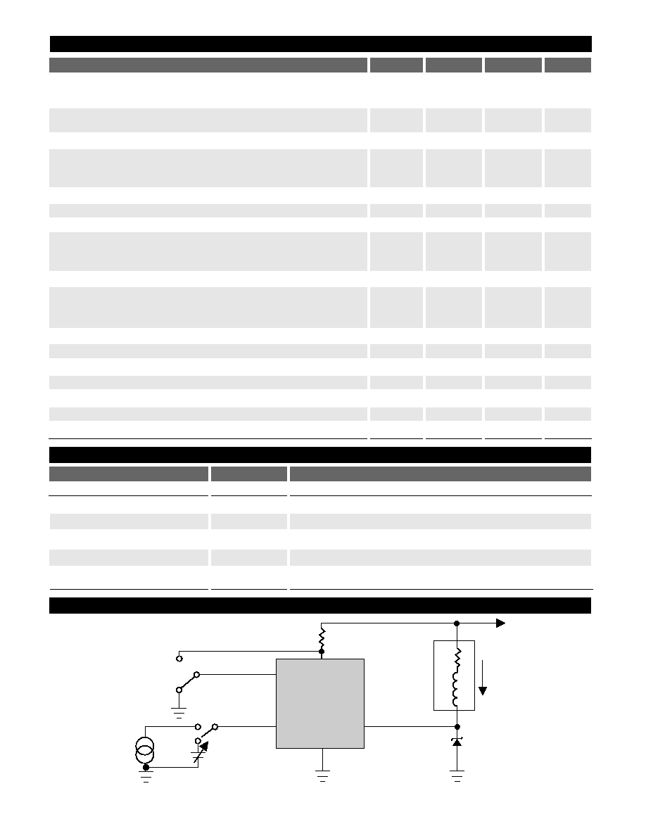
Typical Application Diagram
Absolute Maximum Ratings
Power Supply Voltage (V
CC
) .........................................................................24V
V
IN
..........................................................................................................-6.0 to 24V
Control ..................................................................................................-6.0 to 24V
Peak Transient Voltage (46V Load Dump)..................................................60V
Internal Regulator Current.........................................................................50mA
Junction Temperature Range....................................................-40�C to +150�C
Operating Temperature Range (Tab Temperature) ..............-40�C to +125�C
Storage Temperature Range .....................................................-65�C to +150�C
Lead Temperature Soldering
Wave Solder (through hole styles only)...10 sec. max, 260�C peak
1 V
IN
2 CONTROL
3 Gnd
4 OUT
5 V
CC
Cherry Semiconductor Corporation
2000 South County Trail, East Greenwich, RI 02818
Tel: (401)885-3600 Fax: (401)885-5786
Email: info@cherry-semi.com
Web Site: www.cherry-semi.com
A Company
�
Rev. 12/18/97
2
PACKAGE LEAD #
LEAD SYMBOL
FUNCTION
Electrical Characteristics:
V
BAT
= 12 V
DC
, T
A
= 25�C, test circuit of Test Circuit diagram, unless noted
CHARACTERISTIC
MIN
TYP
MAX
UNIT
CS452/453
CONTROL
Gnd
OUT
CS452/453
V
CC
V
IN
40 V/10 W
Zener
Injector
Load
I
1.2
2.0
mH
R
L
300
W/2W
V
BAT
High
S2
Low
S1
0-5.0 V
DC
5 V
p-p
250Hz
Square
Wave
Test Circuit
Package Lead Description
Output Peak Current (I
pk
)
CS452
1.7
2.4
2.9
A
CS453
3.6
4.4
5.2
A
Output Sustaining Current (I
sus
)
CS452
0.50
0.60
0.70
A
CS453
0.95
1.12
1.25
A
V
(BR)CEO(sus)
@ 1mA
42
50
V
Output Voltage in Saturated Mode
CS452 @ 1.5A
1.2
V
CS453 @ 3.0A
1.6
V
Internal Regulated Voltage
(@V
CC
, Test Circuit diagram)
6.9
V
Input �on� Threshold Voltage
1.4
2.0
V
Input �off� Threshold Voltage
0.7
1.3
V
Input �on� Current
@ V
IN
= 1.4V
DC
35
�A
@ V
IN
= 5.0V
DC
220
�A
CONTROL �on� Threshold Voltage
1.2
1.5
1.8
V
CONTROL Current
CONTROL = 0.8V
DC
-5
-50
�A
CONTROL = 5.0V
DC
1.0
�A
Input Turn On Delay (t
l
)
0.5
1.0
�s
I
pk
sense to I
sus
delay (t
p
)
60
�s
CONTROL Signal Delay (t
t
)
15
�s
Input Turn Off from Saturated Mode Delay (t
s
)
1.0
�s
Input Turn Off from Sustain Mode Delay (t
d
)
0.2
�s
Output Voltage Rise Time (t
v
)
0.4
�s
Output Current Fall Time (t
f
) 4.0A
0.6
1.0
�s
TO-220
1
V
IN
Switches the injector driver on and off.
2
CONTROL
Acts to disable OUT when high.
3
Gnd
Ground connection.
4
OUT
Output Drive current.
5
V
CC
Supply voltage to IC. V
CC
is connected to V
BAT
through a series
resistor (300� typ.)
3
CS452/453
Inductive actuators such as automotive electronic fuel
injectors, relays, solenoids and hammer drivers can be
powered more efficiently by providing a high current
drive until actuation (pull-in) occurs and then decreasing
the drive current to a level which will sustain actuation.
Pull-in and especially dropout times of the actuators are
also improved.
The fundamental output characteristic of the CS452/453
provides a low impedance saturated power switch until
the load current reaches a predetermined high-current
level and then changes to a current source of lower magni-
tude until the device is turned off. This output characteris-
tic allows the inductive load to control its actuation time
during turn-on while minimizing power and stored energy
during the sustain period, thereby promoting a fast turn-
off time.
Automotive injectors at present time come in two types.
The large throttle body injectors have an inductance of
about 2.0mH and an impedance of 1.2� and require the
CS453 driver. The smaller type, popular worldwide, have
an inductance of 4.0mH and an impedance of 2.4� and
needs about a 2.0A pulse for good results, which can be
met with the CS452. Some designs are planned which
employ two of the smaller types in parallel. The induc-
tance of the injectors are much larger at low current,
decreasing due to armature movement and core saturation
to the values above at rated current.
Operating frequencies range from 5.0Hz to 250Hz depend-
ing on the injector location and engine type. Duty cycle in
some designs reaches 80%.
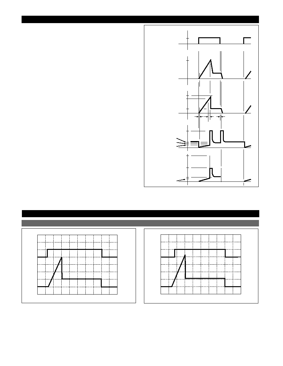
Figure 1. Operating Waveforms (Max. Frequency 250Hz, CONTROL
Grounded)
Circuit Description
>1.4V
0
2.0
4.0ms
Input Signal
V
IN
I
pk
Load
Current
I
pk
Output
Current
I
pk (SENSE)
I
sus
V
Z
V
BAT
V
BAT
- (I
sus
R
L
)
V
SAT
Output
Voltage
V
Z
I
pk
V
Z
I
sus
Power
Dissipation
(V
BAT
- I
sus
R
L
) I
sus
V
SAT
I
pk
t
i
t
p
t
d
Timing Diagrams
Input Voltage and Output Current vs. Time
4
V
IN
(V
olts)
5
0
I
OUT
3
1
0
I
OUT
(Amps)
10
10
9
8
7
6
5
4
3
2
1
0
CS453
2
2.4
V
IN
(V
olts)
5
0
I
OUT
1.8
0.6
0
I
OUT
(Amps)
10
10
9
8
7
6
5
4
3
2
1
0
CS452
1.2
4
CS452/453
The CS452/453 is provided with an input lead (V
IN
) which
turns the injector driver �on� and �off�. This lead has a
nominal trip level of 1.4V and an input impedance of
20k�. It is internally protected against negative voltages
and is compatible with TTL and most other logic.
There is also a control lead (CONTROL) which if held low
or grounded, permits the device to operate in saturation to
I
pk(sense)
, where it will switch to I
sus
automatically. If CON-
TROL is brought high (>1.5V), the output drive stage is
turned off, regardless of what state the input (V
IN
) is at,
and the output current goes to zero.
Figure 1 shows the operating waveforms for the simplest
mode; i.e., with CONTROL grounded. When the driver is
turned on, the current ramps up to the peak current sense
level, where some overshoot occurs because of internal
delay. The CS452/453 then reduces its output to I
sus
. The
fall time of the device is very rapid (�1.0�s), but the decay
of the load current takes 150 to 220 �s, while dumping the
load energy into the protection Zener clamp.
It is essential that the Zener voltage be lower than the
V
(BR)CEO(sus)
, but not so low as to greatly stretch the load
current decay time. Without the zener, the discharge of the
load energy would be totally into the CS452/453, which, for
the high current applications, could cause the device to fail.
Also in figure 1 is the graphically derived instantaneous
power dissipation of the CS452/453. It shows that, for
practical purposes, the worst case dissipation is less than
(I
sus
) (V
BAT
) (duty cycle).
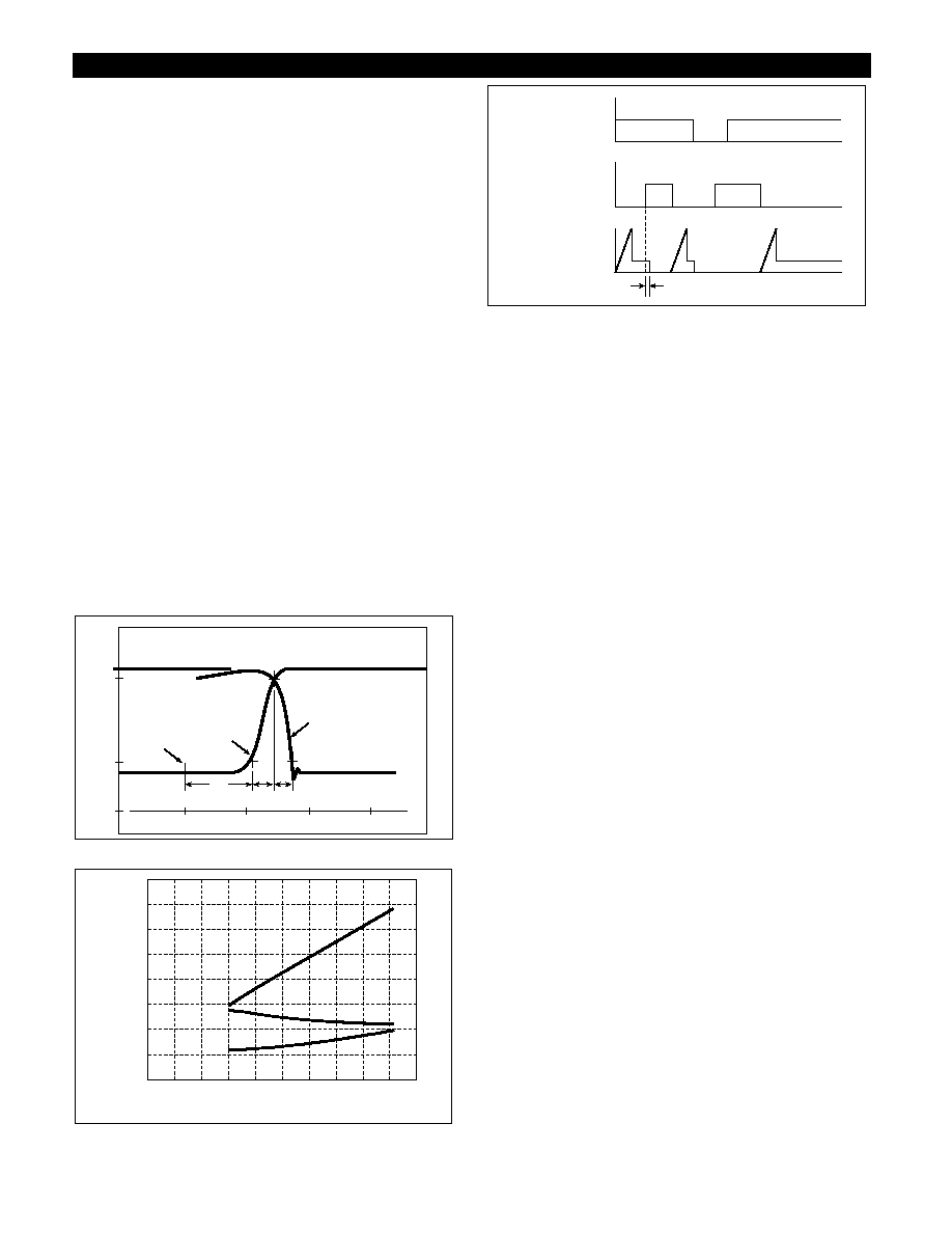
Figure 2. Switching Waveforms (Expanded Time Scale)
Figure3. Switching Speed vs. Temperature
Switching Speed (
m
s)
1.5
140
120
100
80
60
40
20
0
-20
-40
2.0
1.0
0.5
0
Case Temperature (�C)
t
s
t
f
t
v
0
90%
1.0
2.0
3.0
ms
I
pk
10%
0
V
l
Turn
Off
Output
Voltage
Output
Current
t
s
t
v
t
f
Figure 4. Application of CONTROL
Provided in Figures 2,3, and 4 are definitions of the
switching intervals specified in the Electrical
Characteristics. Figure 3 shows that the critical switching
parameters stay under control at elevated temperatures.
In those applications where high voltage transients may
occur while the output lead (OUT) is in the I
sus
mode,
excessive instantaneous power dissipation may occur,
causing device failure. When this condition occurs, the
control lead (CONTROL) can be used to shut off the out-
put stage in order to protect the CS452/453. As long as
CONTROL is in the high state (>1.5 volts, typ.), the output
will remain off. One method of sensing the supply voltage
and controlling CONTROL is to use a resistor divider
between the supply voltage and ground with CONTROL
connected to the resistor divider (see Typical Application
diagram).
Another application option of the control lead is to use it
to accomplish an enable/disable function. Since CON-
TROL is compatible with TTL and CMOS logic levels, a
logic low will enable the output, and allow it to follow the
input signal at V
IN
. If CONTROL is held at a logic high,
the output will be disabled regardless of the state of the
input signal.
If the control function is not being used in the application,
it must be grounded or otherwise placed in a logic low
state. If CONTROL is left open, the output stage will
remain off.
The output current in the I
sus
mode should be oscillation
free. There is a possibility that in a given application, the
output current could oscillate for a small fraction of parts.
If this was to occur, the remedy is place a capacitor from
OUT to Ground. The value of the capacitor should not
exceed 0.01�F.
>1.4V
>1.5V
I
pk
I
sus
Input
Signal
V
IN
Control
Signal
CONTROL
Output
Current
t
l
Application Information
Thermal Data
5 Lead TO-220
R
QJC
typ
2.6
�C/W
R
QJA
typ
50
�C/W
CS452/453
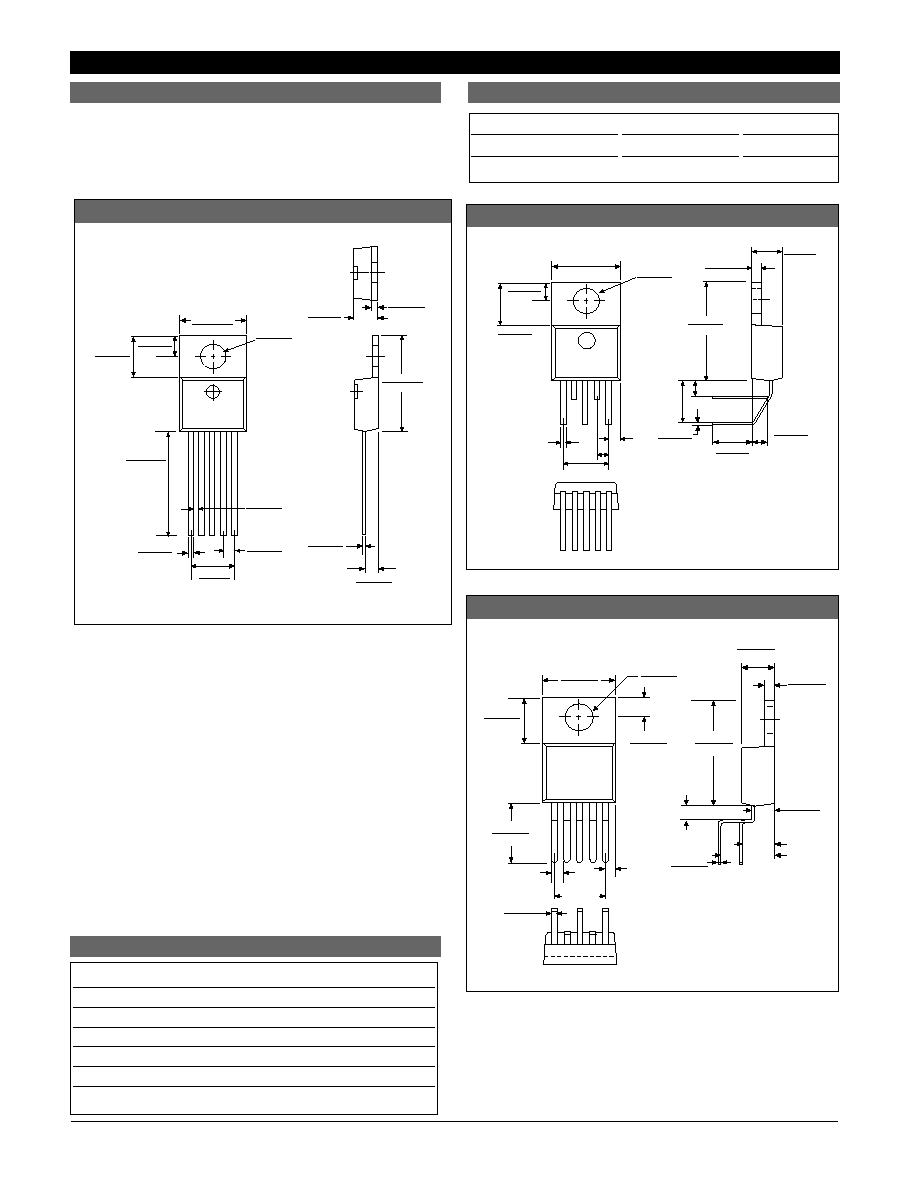
Package Specification
PACKAGE DIMENSIONS IN mm (INCHES)
PACKAGE THERMAL DATA
5
Part Number
Description
CS452GT5
5 Lead TO-220 Straight
CS452GTVA5
5 Lead TO-220 Vertical
CS452GTHA5
5 Lead TO-220 Horizontal
CS453GT5
5 Lead TO-220 Straight
CS453GTVA5
5 Lead TO-220 Vertical
CS453GTHA5
5 Lead TO-220 Horizontal
5 Lead TO-220 (Straight)
2.87 (.113)
2.62 (.103)
6.93(.273)
6.68(.263)
9.78 (.385)
10.54 (.415)
1.02(.040)
0.63(.025)
1.83(.072)
1.57(.062)
0.56 (.022)
0.36 (.014)
2.92 (.115)
2.29 (.090)
1.40 (.055)
1.14 (.045)
4.83 (.190)
4.06 (.160)
6.55 (.258)
5.94 (.234)
14.22 (.560)
13.72 (.540)
1.02 (.040)
0.76 (.030)
3.71 (.146)
3.96 (.156)
14.99 (.590)
14.22 (.560)
Ordering Information
Rev. 12/18/97
� 1999 Cherry Semiconductor Corporation
Cherry Semiconductor Corporation reserves the
right to make changes to the specifications without
notice. Please contact Cherry Semiconductor
Corporation for the latest available information.
5 Lead TO-220 (Horizontal)
0.81(.032)
1.70 (.067)
6.81(.268)
1.40 (.055)
1.14 (.045)
5.84 (.230)
6.60 (.260)
6.83 (.269)
0.56 (.022)
0.36 (.014)
10.54 (.415)
9.78 (.385)
6.55 (.258)
5.94 (.234)
3.96 (.156)
3.71 (.146)
1.68
(.066)
TYP
14.99 (.590)
14.22 (.560)
2.77 (.109)
2.29 (.090)
2.92 (.115)
4.83 (.190)
4.06 (.160)
2.87 (.113)
2.62 (.103)
5 Lead TO-220 (Vertical)
1.68
(.066) typ
1.70 (.067)
7.51 (.296)
1.78 (.070)
4.34 (.171)
0.56 (.022)
0.36 (.014)
1.40 (.055)
1.14 (.045)
4.83 (.190)
4.06 (.160)
14.99 (.590)
14.22 (.560)
2.92 (.115)
2.29 (.090)
.94 (.037)
.69 (.027)
8.64 (.340)
7.87 (.310)
6.80 (.268)
10.54 (.415)
9.78 (.385)
2.87 (.113)
2.62 (.103)
6.55 (.258)
5.94 (.234)
3.96 (.156)
3.71 (.146)