1
Features
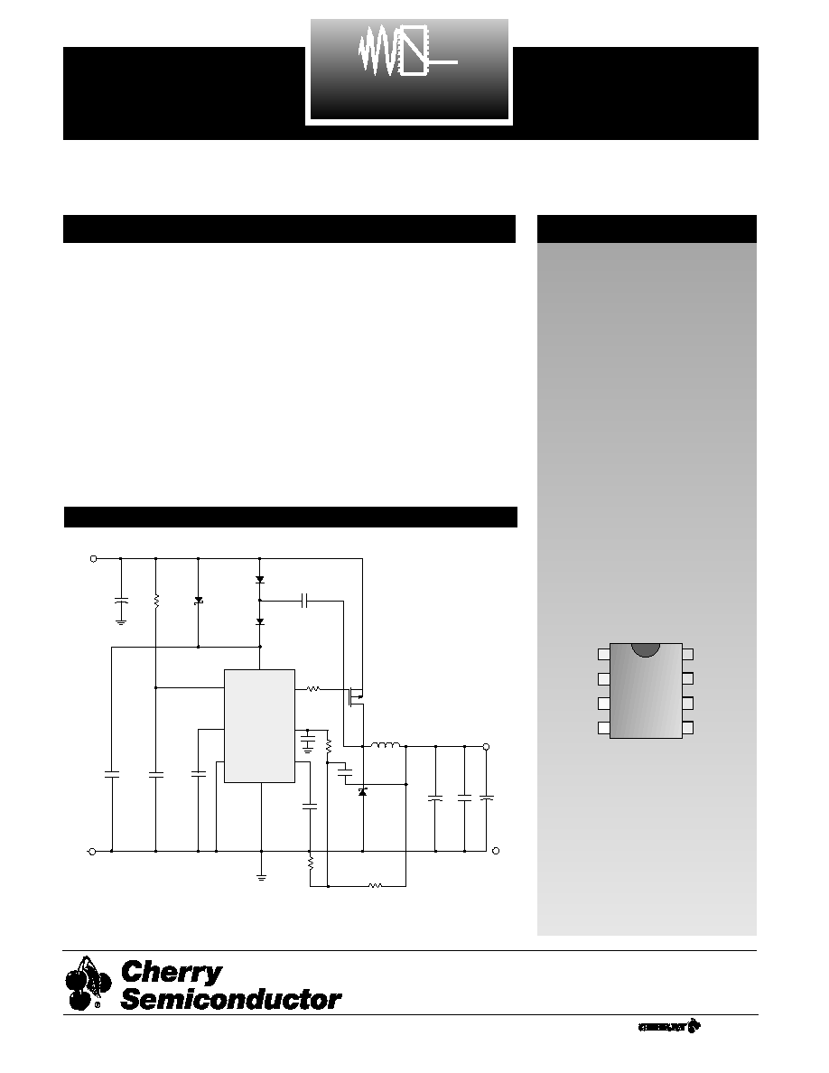
CS
V
FB
V
CC
V
GATE
Gnd
C
OSC
U1
CS51033
C
OSC
150pF
IRF 7404
3.3V
IN
1.5V
OUT
@3Amp
C
1
0.1
µ
F
V
C
PGnd
Gnd
C
3
100
µ
F
C
2
1
µ
F
D
3
1N4148
D
2
1N4148
CS
0.1
µ
F
C
4
C
0
D
1
1N5821
4.7
µ
H
C
IN
100
µ
F
D
4
1N5818
Gnd
R
A
1.5k
R
B
300
NOTE: Capacitors C
2
, C
3
and C
4
are low ESR tantalum
caps used for noise reduction.
R
G
10
R
C
10
.1
µ
F
100
µ
F
100
µ
F
0.1
µ
F
100
0.01
µ
F
s
1A Totem Pole Output
Driver
s
High Speed Oscillator
(700kHz max)
s
No Stability
Compensation Required
s
Lossless Short Circuit
Protection
s
2% Precision Reference
s
Programmable Soft Start
Package Options
CS51033
Fast PFET Buck Controller
Does Not Require Compensation
CS51033
Description
The CS51033 is a switching con-
troller for use in DC-DC converters.
It can be used in the buck topology
with a minimum number of exter-
nal components. The CS51033 con-
sists of a 1.0A power driver for con-
trolling the gate of a discrete P-
channel transistor, fixed frequency
oscillator, short circuit protection
timer, programmable soft start, pre-
cision reference, fast output voltage
monitoring comparator, and output
stage driver logic with latch.
The high frequency oscillator
allows the use of small inductors
and output capacitors, minimizing
PC board area and systems cost.
The programmable soft start
reduces current surges at start up.
The short circuit protection timer
significantly reduces the PFET duty
cycle to approximately 1/30 of its
normal cycle during short circuit
conditions.
The CS51033 is available in 8L SO
and 8L PDIP plastic packages.
Typical Application Diagram
1
V
GATE
PGnd
C
OSC
Gnd
V
C
CS
V
CC
V
FB
8 Lead SO Narrow & PDIP
A Company
Æ
Rev. 2/13/98
Cherry Semiconductor Corporation
2000 South County Trail, East Greenwich, RI 02818
Tel: (401)885-3600 Fax: (401)885-5786
Email: info@cherry-semi.com
Web Site: www.cherry-semi.com

Power Supply Voltage, V
CC
..........................................................................................................................................................5V
Driver Supply Voltage, V
C
..........................................................................................................................................................20V
Driver Output Voltage, V
GATE
...................................................................................................................................................20V
C
OSC
, CS, V
FB
(Logic Pins) ............................................................................................................................................................5V
Peak Output Current................................................................................................................................................................. 1.0A
Steady State Output Current ................................................................................................................................................200mA
Operating Junction Temperature, T
J
..................................................................................................................................... 150∞C
Storage Temperature Range, T
S
...................................................................................................................................-65 to 150∞C
ESD (Human Body Model).........................................................................................................................................................2kV
Lead Temperature Soldering
Wave Solder (through hole styles only) .....................................................................................10 sec. max, 260∞C peak
Reflow (SMD styles only) ......................................................................................60 sec. max above 183∞C, 230∞C peak
PARAMETER
TEST CONDITIONS
MIN
TYP
MAX
UNIT
2
CS51033
Absolute Maximum Ratings
Electrical Characteristics: Specifications apply for 3.135 V
CC
3.465V, 3V V
C
16V,
-40∞C T
A
125∞C, -40∞C T
J
125∞C, unless otherwise specified.
s
Oscillator
V
FB
= 1.2V
Frequency C
OSC
= 470pF
160
200
240
kHz
Charge Current
1.4V < V
COSC
< 2V
110
µA
Discharge Current
2.7V > V
COSC
> 2V
660
µA
Maximum Duty Cycle
1 ≠ (t
OFF
/t
ON
)
80.0
83.3
%
s
Short Circuit Timer
V
FB
= 1.0V; CS = 0.1µF; V
COSC
= 2V
Charge Current
1V < V
CS
< 2V
175
264
325
µA
Fast Discharge Current
2.55V > V
CS
> 2.4V
40
66
80
µA
Slow Discharge Current
2.4V > V
CS
> 1.5V
4
6
10
µA
Start Fault Inhibit Time
0.70
0.85
1.40
ms
Valid Fault Time
2.6V > V
CS
> 2.4V
0.2
0.3
0.45
ms
GATE Inhibit Time
2.4V > V
CS
> 1.5V
9
15
23
ms
Duty Cycle
2.5
3.1
4.6
%
s
CS Comparator
V
FB
= 1V
Fault Enable CS Voltage
2.5
V
Max. CS Voltage
V
FB
= 1.5V
2.6
V
Fault Detect Voltage
V
CS
when GATE goes high
2.4
V
Fault Inhibit Voltage
Minimum V
CS
1.5
V
Hold Off Release Voltage
V
FB
= 0V
0.4
0.7
1.0
V
Regulator Threshold
V
CS
= 1.5V
0.725
0.866
1.035
V
Voltage Clamp
s
V
FB
Comparator
V
COSC
= V
CS
= 2V
Regulator Threshold Voltage T
J
= 25∞C (Note 1)
1.225
1.250
1.275
V
T
J
= -40 to 125∞C
1.210
1.250
1.290
V
Fault Threshold Voltage
T
J
= 25∞C (Note 1)
1.12
1.15
1.17
V
T
J
= -40 to 125∞C
1.10
1.15
1.19
V
Threshold Line Regulation
3.135V V
CC
3.465
6
15
mV
Input Bias Current
V
FB
= 0V
1
4
µA
Voltage Tracking
(Regulator Threshold Voltage -
70
100
120
mV
Fault Threshold Voltage)
Input Hysteresis Voltage
4
20
mV

PARAMETER
TEST CONDITIONS
MIN
TYP
MAX
UNIT
CS51033
3
Package Pin Description
PACKAGE PIN #
PIN SYMBOL
FUNCTION
Electrical Characteristics: Specifications apply for 3.135 V
CC
3.465V, 3V V
C
16V,
-40∞C T
J
125∞C, unless otherwise specified.
8L SO Narrow & PDIP
1
V
GATE
Driver pin to gate of external PFET.
2
PGnd
Output power stage ground connection.
3
C
OSC
Oscillator frequency programming capacitor.
4
Gnd
Logic ground.
5
V
FB
Feedback voltage input.
6
V
CC
Logic supply voltage.
7
CS
Soft start and fault timing capacitor.
8
V
C
Driver supply voltage.
s
Power Stage
V
C
= 10V; V
FB
= 1.2V
GATE DC Low Saturation
V
COSC
= 1V; 200mA Sink
1.2
1.5
V
Voltage
GATE DC High Saturation
V
COSC
= 2.7V; 200mA Source; V
C
= V
GATE
1.5
2.1
V
Voltage
Rise Time
C
GATE
= 1nF; 1.5V < V
GATE
< 9V
25
60
ns
Fall Time
C
GATE
= 1nF; 9V > V
GATE
> 1.5V
25
60
ns
s
Current Drain
I
CC
3.135V < V
CC
< 3.465V, Gate switching
3.5
6.0
mA
I
C
3V < V
C
< 16V, Gate non-switching
2.7
4.0
mA
Note1: Guaranteed by design not 100% tested in production.
CS51033
4
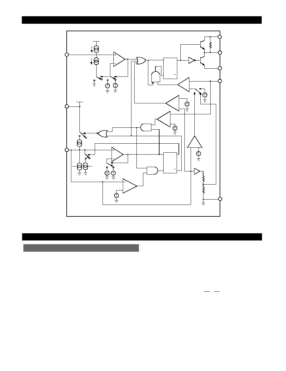
Block Diagram
G5
C
OSC
CS
V
CC
V
C
V
GATE
PGnd
V
FB
Gnd
R
S
2.5V
1.5V
1.25V
1.15V
Q
F2
G2
G1
A1
A6
RG
V
CC
A3
2.4V
G3
A2
2.5V
1.5V
I
C
7I
C
V
CC
+
-
I
T
+
Q
I
T
5
I
T
55
G4
Fault
Comp
+
-
+
-
+
-
A4
0.7V
2.3V
Q
R
Q
S
F1
Slow Discharge
Comparator
Slow Discharge
Flip-Flop
CS Charge
Sense
Comparator
CS
Comparator
Oscillator
Comparator
V
FB
Comparator
V
GATE
Flip-Flop
Hold
Off
Comp
Control Scheme
The CS51033 monitors the output voltage to determine
when to turn on the PFET. If V
FB
falls below the internal ref-
erence voltage of 1.25V during the oscillator's charge cycle,
the PFET is turned on and remains on for the duration of the
charge time. The PFET gets turned off and remains off dur-
ing the oscillator's discharge cycle time with the maximum
duty cycle to 80%. It requires 7mV typical, and 20mV maxi-
mum ripple on the V
FB
pin is required to operate. This
method of control does not require any loop stability com-
pensation.
Startup
The CS51033 has an externally programmable soft start fea-
ture that allows the output voltage to come up slowly, pre-
venting voltage overshoot on the output.
At startup, the voltage on all pins is zero. As V
CC
rises, the
V
C
voltage along with the internal resistor R
G
keeps the
PFET off. As V
CC
and V
C
continue to rise, the oscillator
capacitor (C
OSC
) and the Soft start/Fault Timing capacitor
(CS) charges via internal current sources. C
OSC
gets charged
by the current source I
C
and CS gets charged by the I
T
source combination described by:
I
CS
= I
T
-
(
+
)
The internal Holdoff Comparator ensures that the external
PFET is off until V
CS
> 0.7V preventing the GATE flip-flop
(F2) from being set. This allows the oscillator to reach its
operating frequency before enabling the drive output. Soft
start is obtained by clamping the V
FB
comparator's (A6) ref-
erence input to approximately 1/2 of the voltage at the CS
pin during startup, permitting the control loop and the out-
put voltage to slowly increase. Once the CS pin charges
above the Holdoff Comparator trip point of 0.7V, the low
I
T
5
I
T
55
Theory of Operation
Circuit Description
Figure 1: Block Diagram for CS51033

CS51033
5
Circuit Description: continued
Applications Information
Specifications
V
IN
= 3.3V +/- 10% (i.e. 3.63V max., 2.97V min.)
V
OUT
= 1.5V +/- 2%
I
OUT
= 0.3A to 3A
Output ripple voltage < 33mV.
F
SW
= 200kHz.
1) Duty Cycle Estimates
Since the maximum duty cycle, D, of the CS51033 is limited
to 80% min. it is best to estimate the duty cycle for the vari-
ous input conditions to see that the design will work over
the complete operating range.
The duty cycle for a buck regulator operating in a continu-
ous conduction mode is given by:
D =
Where V
SAT
is Rdson ◊ I
OUT
Max.
In this case we can assume that V
D
= 0.6V and V
SAT
= 0.6V
so the equation reduces to:
V
OUT
+ V
D
V
IN -
V
SAT
Designing a Power Supply with the CS51033
feedback to the V
FB
Comparator sets the GATE flip-flop dur-
ing C
OSC
's charge cycle. Once the GATE flip-flop is set,
V
GATE
goes low and turns on the PFET. When V
CS
exceeds
2.4V, the CS charge sense comparator (A4) sets the V
FB
com-
parator reference to 1.25V completing the startup cycle.
Lossless Short Circuit Protection
The CS51033 has "Lossless" short circuit protection since
there is no current sense resistor required. When the voltage
at the CS pin (the fault timing capacitor voltage ) reaches
2.5V, the fault timing circuitry is enabled. During normal
operation the CS voltage is 2.6V. During a short circuit con-
dition or a transient condition, the output voltage moves
lower and the voltage at V
FB
drops. If V
FB
drops below
1.15V, the output of the fault comparator goes high and the
CS51033 goes into a fast discharge mode. The fault timing
capacitor, CS, discharges to 2.4V. If the V
FB
voltage is still
below 1.15V when the CS pin reaches 2.4V, a valid fault con-
dition has been detected. The slow discharge comparator
output goes high and enables gate G5 which sets the slow
discharge flip flop. The Vgate flip flop resets and the output
switch is turned off. The fault timing capacitor is slowly dis-
charged to 1.5V. The CS51033 then enters a normal startup
routine. If the fault is still present when the fault timing
capacitor voltage reaches 2.5V, the fast and slow discharge
cycles repeat as shown in figure 2.
If the V
FB
voltage is above 1.15V when CS reaches 2.4V a
fault condition is not detected, normal operation resumes
and CS charges back to 2.6V. This reduces the chance of
erroneously detecting a load transient as a fault condition.
Figure 2. Voltage on start capacitor (V
GS
), the gate (V
GATE
), and in the
feedback loop (V
FB
), during startup, normal and fault conditions.
Buck Regulator Operation
Figure 3. Buck regulator block diagram.
A block diagram of a typical buck regulator is shown in
Figure 3. If we assume that the output transistor is initially
off, and the system is in discontinuous operation, the induc-
tor current I
L
is zero and the output voltage is at its nominal
value. The current drawn by the load is supplied by the out-
put capacitor C
O
. When the voltage across C
O
drops below
the threshold established by the feedback resistors R1 and
R2 and the reference voltage V
REF
, the power transistor Q1
switches on and current flows through the inductor to the
output. The inductor current rises at a rate determined by
(V
IN
-V
OUT
)/Load. The duty cycle (or "on" time) for the
CS51033 is limited to 80%. If the output voltage remains
higher than nominal during the entire C
OSC
charge time, the
Q1 does not turn on, skipping the pulse.
CHARGE PUMP CIRCUIT
(Refer to the CS51033 Application Diagram)
An external charge pump circuit is necessary when the input
voltage is below 5V to ensure that there is sufficient gate
drive voltage for the external FET. When V
IN
is applied,
capacitors C1 and C2 will be charged to a diodes drop below
V
IN
via diodes D2 and D4, respectively. When the PFET
turns on, its drain voltage will be approximately equal to
V
IN
. Since the voltage across C1 can not change instanta-
neously, D2 is reverse biased and the anode voltage rises to
approximately 2*3.3V-VD2. C1 transfers some of its stored
charge C2 via D3. After several cycles there is sufficient gate
drive voltage.
Control
Feedback
V
IN
L
D
1
R
1
R
2
R
LOAD
C
O
Q1
C
IN
2.5V
0V
FAULT
NORMAL OPERATION
START
T
START
td1
td2
t
FAULT
t
RESTART
t
FAULT
S2
S2
S2
S3
S3
S3
S3
S1
S1
S1
2.6V
2.4V
1.5V
0V
1.25V
1.15V
V
CS
V
GATE
V
FB