1
Features
s
Linear Regulator
5V ± 2% @ 100mA
s
Switching Regulator
1.4A Peak Internal
Switch
120kHz Maximum
Switching Frequency
5V to 26V Operating
Supply Range
s
Smart Functions
Watchdog
s
Protection
Overvoltage
Overtemperature
Current Limit
s
54V Peak Transient
Capability
ENABLE
RESET
Package Option
24 Lead SO Wide
(Internally Fused Leads)
CS5111
1.4A Switching Regulator with 5V, 100mA Linear
Regulator with Watchdog, RESET and ENABLE
1
V
REG
V
LIN
I
BIAS
Gnd
Gnd
Gnd
Gnd
RESET
C
Delay
WDI
C
OSC
V
IN
NC
NC
V
SW
Gnd
Gnd
Gnd
Gnd
V
FB1
V
FB2
SELECT
COMP
ENABLE
CS5111
Description
Over
Temperature
V
IN
Linear
Error Amplifier
1.25V
V
REG
1.4A
V
SW
COMP
V
FB1
V
FB2
SELECT
V
LIN
I
BIAS
C
DELAY
Over Voltage
RESET &
Watchdog Timer
Current
Limit
WDI
C
OSC
Base
Drive
RESET
Gnd
Bandgap
Reference
Oscillator
Multiplexer
+
-
COMP
Logic
+
-
+
-
+
-
Switcher Shutdown
Switcher
Error Amplifier
Current Sense Amplifier
ENABLE
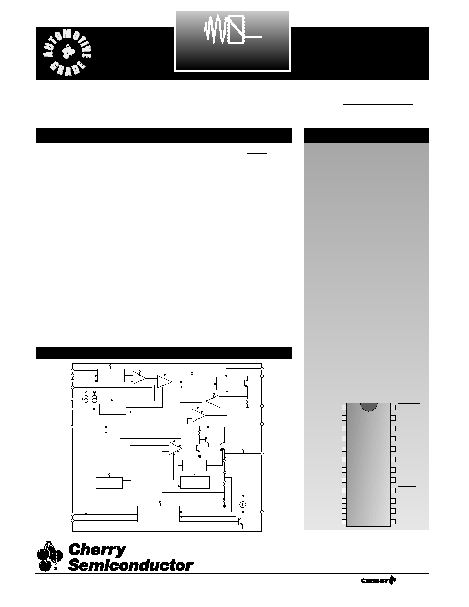
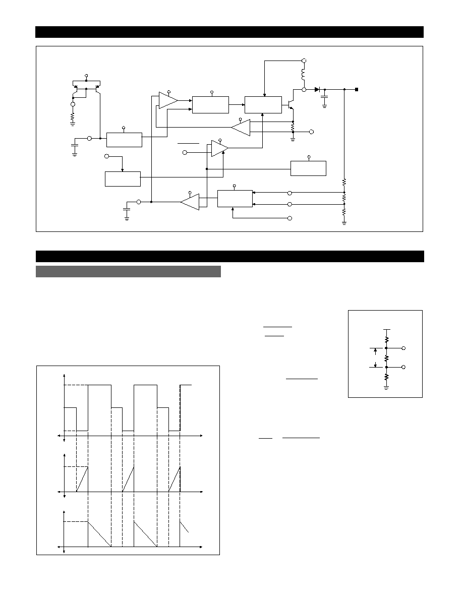
Block Diagram
The CS5111 is a dual output power sup-
ply integrated circuit. It contains a 5V
±2%, 100mA linear regulator, a watchdog
timer, a linear output voltage monitor to
provide a Power On Reset (POR) and a
1.4A current mode PWM switching reg-
ulator.
The 5V linear regulator is comprised of
an error amplifier, reference, and super-
visory functions. It has low internal sup-
ply current consumption and provides
1.2V (typical) dropout voltage at maxi-
mum load current.
The watchdog timer circuitry monitors
an input signal (WDI) from the micro-
processor. It responds to the falling
edge of this watchdog signal. If a correct
watchdog signal is not received within
the externally programmable time, a
reset signal is issued.
The externally programmable active
reset circuit operates correctly for an out-
put voltage (V
LIN
) as low as 1V. During
power up, or if the output voltage shifts
below the regulation limit,
tog-
gles low and remains low for the duration
of the delay after proper output voltage
regulation is restored. Additionally a reset
pulse is issued if the correct watchdog is
not received within the programmed
time. Reset pulses continue until the cor-
rect watchdog signal is received. The
reset pulse width and frequency, as well
as the Power On Reset delay, are set by
one external RC network.
The current mode PWM switching regu-
lator is comprised of an error amplifier
with selectable feedback inputs, a cur-
rent sense amplifier, an adjustable oscil-
lator, and a 1.4A output power switch
with anti-saturation control. The switch-
ing regulator can be configured in a
variety of topologies.
The CS5111 is load dump capable and
has protection circuitry which includes
overvoltage shutdown, current limit on
the linear and switcher outputs, and an
overtemperature limiter.
RESET
Rev. 12/28/98
Cherry Semiconductor Corporation
2000 South County Trail, East Greenwich, RI 02818
Tel: (401)885-3600 Fax: (401)885-5786
Email: info@cherry-semi.com
Web Site: www.cherry-semi.com
A Company
Æ

2
CS5111
PARAMETER
TEST CONDITIONS
MIN
TYP
MAX
UNIT
Absolute Maximum Ratings
Logic Inputs/Outputs (
, SELECT, WDI,
) ................................................................................-0.3V to V
LIN
V
LIN
................................................................................................................................................................................-0.3V to 10V
V
IN
, V
REG:
DC Input Voltage .................................................................................................................................................-0.3V to 26V
Peak Transient Voltage (40V Load Dump @ 14V V
IN
)....................................................................................-0.3V to 54V
V
SW
Peak Transient Voltage .....................................................................................................................................................54V
C
OSC
, C
Delay
, COMP,V
FB1
, V
FB2
..................................................................................................................................-0.3V to V
LIN
Power Dissipation.............................................................................................................................................Internally Limited
V
LIN
Output Current ........................................................................................................................................Internally Limited
V
SW
Output Current .........................................................................................................................................Internally Limited
Output Sink Current ..................................................................................................................................................5mA
ESD Susceptibility (Human Body Model)..............................................................................................................................2kV
ESD Susceptibility (Machine Model).....................................................................................................................................200V
Storage Temperature...................................................................................................................................................-65 to 150∞C
Lead Temperature Soldering: Reflow (SMD styles only) ..........................................60 sec. max above 183∞C, 230∞C peak
RESET
RESET
ENABLE
Electrical Characteristics: 5V V
IN
26V and -40∞C T
J
150∞C, C
OUT
= 100µF (ESR8), C
Delay
= 0.1µF, R
BIAS
= 64.9k,
C
OSC
= 390 pF, C
COMP
= 0.1µF unless otherwise specified.
s
General
I
IN
Off Current
6.6V V
IN
26V, I
SW
= 0A
2.0
mA
I
IN
On Current
6.6V V
IN
26V, I
SW
= 1.4A
30
70
mA
I
REG
Current
I
LIN
= 100mA, 6.6V V
REG
26V
6
mA
Thermal Limit
Guaranteed by design
160
210
∞C
s
5V Regulator Section
V
LIN
Output Voltage
6.6V V
REG
26V, 1mA I
LIN
100mA
4.9
5.0
5.1
V
Dropout Voltage
(V
REG
- V
LIN
) @ I
LIN
= 100mA
1.2
1.5
V
Overvoltage Shutdown
30
34
38
V
Line Regulation
6.6V V
REG
26V, I
LIN
= 5mA
5
25
mV
Load Regulation
V
REG
= 19V, 1mA I
LIN
100mA
5
25
mV
Current Limit
6.6V V
REG
26V
120
mA
DC Ripple Rejection
14V V
REG
24V
60
75
dB
s
Section
Low Threshold (V
RTL
)
V
LIN
Decreasing
4.05
4.25
4.45
V
High Threshold (V
RTH
)
V
LIN
Increasing
4.20
4.45
4.70
V
Hysteresis
V
RTH
- V
RTL
140
190
240
mV
Active High
V
LIN
> V
RTH
, I
RESET
= -25µA
V
LIN
- 0.5
V
Active Low
V
LIN
= 1V, 10k pullup from
to V
LIN
0.4
V
V
LIN
= 4V, I
RESET
= 1mA
0.7
V
Delay Invalid
WDI
6.25
8.78
11.0
ms
Power On Delay
V
LIN
crossing V
RTH
6.25
ms
RESET
RESET

3
PARAMETER
TEST CONDITIONS
MIN
TYP
MAX
UNIT
CS5111
Electrical Characteristics: 5V V
IN
26V and -40∞C T
J
150∞C, C
OUT
=100µF(ESR 8), C
Delay
= 0.1µF, R
BIAS
= 64.9k,
C
OSC
= 390 pF, C
COMP
= 0.1µF unless otherwise specified.
s
Watchdog Input (WDI)
VIH
Peak WDI needed to activate
2.0
V
VIL
0.8
V
Hysteresis
Note 1
25
50
mV
Pull-Up Resistor
WDI=0V
20
50
100
k
Low Threshold
6.25
8.78
11.0
ms
Floating Input Voltage
3.5
V
WDI Pulse Width
5
µs
s
Switcher Section
Minimum Operating
5.0
V
Input Voltage
Switching Frequency
Refer to Figure 1d.
80
95
110
kHz
Switch Saturation Voltage
I
SW
= 1.4A
0.7
1.1
1.6
V
Output Current Limit
1.4
2.5
A
Max Switching Frequency
V
SW
= 7.5V with 50 load, 120
kHz
Refer to Figure 1d.
V
FB1
Regulation Voltage
1.206
1.25
1.294
V
V
FB2
Regulation Voltage
1.206
1.25
1.294
V
V
FB1
, V
FB2
Input Current
V
FB1
= V
FB2
= 5V
1
µA
Oscillator Charge Current
C
OSC
= 0V
35
40
45
µA
Oscillator Discharge Current C
OSC
= 4V
270
320
370
µA
C
Delay
Charge Current
C
Delay
= 0V
35
40
45
µA
Switcher Max Duty Cycle
V
SW
= 5V with 50 load, 72
85
95
%
V
FB1
= V
FB2
= 1V
Current Sense Amp Gain
I
SW
= 2.3A
7
Error Amp DC Gain
67
dB
Error Amp Transconductance
2700
µA/V
s
Input
VIL
0.8
1.24
V
VIH
1.30
2.0
V
Hysteresis
60
mV
Input Impedance
10
20
40
k
s
Select Input
VIL (Selects V
FB1
)
4.9 V
LIN
5.1
0.8
1.25
V
VIH (Selects V
FB2
)
4.9 V
LIN
5.1
1.25
2.0
V
SELECT Pull-Up
SELECT = 0V
10
24
50
k
Floating Input Voltage
3.5
4.5
V
Note 1: Guaranteed by Design, not 100% tested in production.
ENABLE
RESET
4
Typical Performance Characteristics
0A
20mA
40mA
60mA
80mA
100mA
3.5mA
4.0mA
4.5mA
I
LIN
I
REG
- I
LIN
-30mA
-40mA
0A
0.5A
I
SW
-20mA
-10mA
0A
1.0A
1.5A
2.0A
I
IN
ISW
0A
0.5A
1.0A
1.5A
2.0A
0.4V
0.0V
0.6V
0.8V
1.2V
1.0V
V
SW
0.2V
1.4V
Package Lead Description
PACKAGE LEAD #
LEAD SYMBOL
FUNCTION
CS5111
40
0
0
C
OSC
(pF)
80
120
160
1000
Frequency (kHz)
20
60
100
140
2000
3000
500
1500
2500
180
Figure 1a. 5V Regulator Bias Current vs. Load Current.
Figure 1b. Supply Current vs. Switch Current.
Figure 1c. Switch Saturation Voltage.
Figure 1d. Oscillator Frequency (kHz) vs. C
OSC
(pF), assuming R
BIAS
=
64.9k.
24 Lead SO Wide
1
V
IN
Supply Voltage.
2, 3
NC
No connection.
4
V
SW
Collector of NPN power switch for switching regulator section.
5,6,7,8,17,18,19,20
Gnd
Connected to the heat removing leads.
9
V
FB1
Feedback input voltage 1 (referenced to 1.25V)
10
V
FB2
Feedback input voltage 2 (referenced to 1.25V)
11
SELECT
Logic level input that selects either V
FB1
or V
FB2
. An open selects
V
FB2
. Connect to Gnd to select V
FB1
.
12
COMP
Output of the transconductance error amplifier.
13
C
OSC
A capacitor connected to Gnd sets the switching frequency.
Refer to Figure 1d.
14
WDI
Watchdog input. Active on falling edge.
15
C
Delay
A capacitor connected to Gnd sets the Power On Reset and
Watchdog time.
16
output. Active low if V
LIN
is below the regulation limit.
If watchdog timeout is reached, a reset pulse train is issued.
21
I
BIAS
A resistor connected to Gnd sets internal bias currents as well as
the C
OSC
and C
Delay
charge currents.
22
V
LIN
Regulated 5V output from the linear regulator section.
23
V
REG
Input voltage to the linear regulator and the internal supply cir-
cuitry.
24
Logic level input to shut down the switching regulator.
ENABLE
RESET
RESET
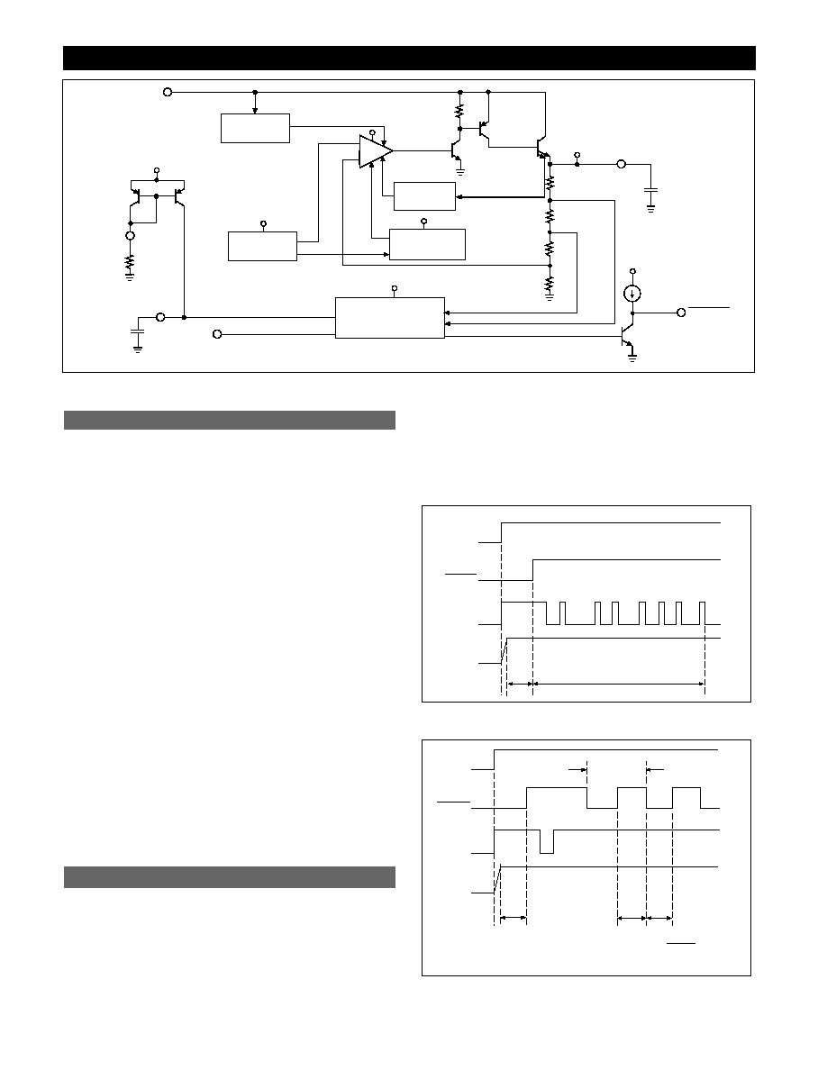
The 5V linear regulator consists of an error amplifier,
bandgap voltage reference, and a composite pass transistor.
The 5V linear regulator circuitry is shown in Figure 2.
When an unregulated voltage greater than 6.6V is applied
to the V
REG
input, a 5V regulated DC voltage will be pre-
sent at V
LIN
. For proper operation of the 5V linear regula-
tor, the I
BIAS
lead must have a 64.9k pull down resistor to
ground. A 100µF or larger capacitor with an ESR <8
must be connected between V
LIN
and ground. To operate
the 5V linear regulator as an independent regulator (i.e.
separate from the switching supply), the input voltage
must be tied to the V
REG
lead.
As the voltage at the V
REG
input is increased, Q
1
is turned
on. Q
1
provides base drive for Q
2
which in turn provides
base current for Q
3
. As Q
3
is turned on, the output voltage,
V
LIN
, begins to rise as Q
3
's output current charges the out-
put capacitor, C
OUT
. Once V
LIN
rises to a certain level, the
error amplifier becomes biased and provides the appropri-
ate amount of base current to Q
1
. The error amplifier mon-
itors the scaled output voltage via an internal voltage
divider, R
2
through R
5
, and compares it to the bandgap
voltage reference. The error amplifier output or error sig-
nal is an output current equal to the error amplifier's input
differential voltage times the transconductance of the
amplifier. Therefore, the error amplifier varies the base
current to Q
1
, which provides bias to Q
2
and Q
3
, based on
the difference between the reference voltage and the
scaled V
LIN
output voltage.
The watchdog timer circuitry monitors an input signal
(WDI) from the microprocessor. It responds to the falling
edge of this watchdog signal which it expects to see within
an externally programmable time (see Figure 3).
The watchdog time is given by:
t
WDI
= 1.353 ◊ C
Delay
R
BIAS
Using C
Delay
= 0.1µF and R
BIAS
= 64.9k gives a time rang-
ing from 6.25ms to 11ms assuming ideal components. Based
on this, the software must be written so that the watchdog
arrives at least every 6.25ms. In practice, the tolerance of
C
Delay
and R
BIAS
must be taken into account when calculat-
ing the minimum watchdog time (t
WDI
).
Figure 3. Timing diagram for normal regulator operation.
Figure 4. Timing diagram when WDI fails to appear within the preset
time interval, t
WDI
.
V
LIN
WDI
RESET
V
REG
t
POR
A
B
A: Watchdog waiting for
low-going transition on
WDI
50% Duty
Cycle
B: RESET stays low for
t
WDI
time.
V
LIN
WDI
RESET
V
REG
t
POR
Normal Operation
Control Functions
5V Linear Regulator
Circuit Description
CS5111
Over
Temperature
Linear
Error
Amplifier
1.25V
V
REG
V
LIN
C
delay
Over Voltage
RESET &
Watchdog Timer
Current
Limit
WDI
RESET
Bandgap
Reference
+
-
I
BIAS
R
BIAS
64.9k
R
1
R
2
R
3
R
4
R
5
C
OUT
= 100
µ
F
ESR < 8
Q
1
Q
2
Q
3
Figure 2. Block diagram of 5V linear regulator portion of the CS5111.
5
6
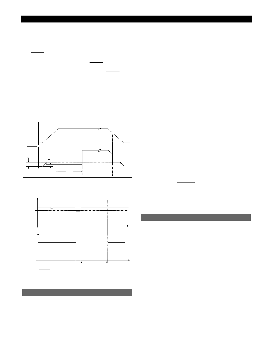
Circuit Description: continued
CS5111 If a correct watchdog signal is not received within the
specified time a reset pulse train is issued until the correct
watchdog signal is received. The nominal reset signal in
this case is a 5 volt square wave with a 50% duty cycle as
shown in Figure 4.
The
signal frequency is given by:
f
RESET
=
The Power On Reset (POR) and low voltage
use
the same circuitry and issue a reset when the linear output
voltage is below the regulation limit. After V
LIN
rises
above the minimum specified value,
remains low
for a fixed period t
POR
as shown in Figure 5.
The POR delay (t
POR
) is given by:
t
POR
= 1.353 ◊ C
Delay
R
BIAS
Figure 5a. The power on reset time interval (t
POR
) begins when V
LIN
rises above 4.45V (typical).
Figure 5b.
signal is issued whenever V
LIN
falls below 4.25V
(typical).
The current mode PWM switching voltage regulator con-
tains an error amplifier with selectable feedback inputs, a
current sense amplifier, an adjustable oscillator and a 1.4A
output power switch with antisaturation control. The
switching regulator and external components, connected
in a boost configuration, are shown in Figure 6.
The switching regulator begins operation when V
REG
and
V
IN
are raised above 5 volts. V
REG
is required since the
switching supply's control circuitry is powered through
V
LIN
. V
IN
supplies the base drive to the switcher output
transistor.
The output transistor turns on when the oscillator starts to
charge the capacitor on C
OSC
. The output current will
develop a voltage drop across the internal sense resistor
(R
S
). This voltage drop produces a proportional voltage at
the output of the current sense amplifier, which is com-
pared to the output of the error amplifier. The error ampli-
fier generates an output voltage which is proportional to
the difference between the scaled down output boost volt-
age (V
FB1
or V
FB2
)
and the internal bandgap voltage refer-
ence. Once the current sense amplifier output exceeds the
error amplifier's output voltage, the output transistor is
turned off.
The energy stored in the inductor during the output tran-
sistor on time is transferred to the load when the output
transistor is turned off. The output transistor is turned
back on at the next rising edge of the oscillator. On a cycle
by cycle basis, the current mode controller in a discontinu-
ous mode of operation charges the inductor to the appro-
priate amount of energy, based on the energy demand of
the load. Figure 7 shows the typical current and voltage
waveforms for a boost supply operating in the discontinu-
ous mode.
NOTES:
1. Refer to Figure 1d to determine oscillator frequency.
2. The switching regulator can be disabled by providing a
logic high at the
input.
3. The boost output voltage can be controlled dynamically
by the feedback select input. If select is open, V
FB2
is
selected. If select is low, then V
FB1
is selected.
If the input voltage at V
REG
is increased above the over-
voltage threshold, the drive to the linear and switcher out-
put transistors is shut off. Therefore, V
LIN
is disabled and
V
SW
can not be pulled low.
The current out of V
LIN
is sensed in order to limit exces-
sive power dissipation in the linear output transistor over
the output range of 0V to regulation. Also, the current into
V
SW
is sensed in order to provide the current limit func-
tion in the switcher output transistor.
If the die temperature is increased above 160∞C, either due
to excessive ambient temperature or excessive power dis-
sipation, the drive to the linear output transistor is
reduced proportionally with increasing die temperature.
Therefore, V
LIN
will decrease with increasing die tempera-
ture above 160∞C. Since the switcher control circuitry is
powered through V
LIN
, the switcher performance, includ-
ing current limit, will be affected by the decrease in V
LIN
.
Protection Circuitry
ENABLE
Current Mode PWM Switching Circuitry
RESET
5V
4.25V
RESET
5V
t
POR
V
LIN
V
LIN
4.45V
4.25V
V
RLO
t
POR
RESET
V
RPEAK
RESET
RESET
1
2(t
WDI
)
RESET
7
Application Notes
CS5111
Circuit Description: continued
This section outlines a procedure for designing a boost switch-
ing power supply operating in the discontinuous mode.
Step 1
Determine the output power required by the load.
P
OUT
= I
OUT
V
OUT
(1)
Step 2
Choose C
OSC
based on the target oscillator frequency with an
external resistor value, R
BIAS
= 64.9k. (See Figure 1d).
Figure 7: Voltage and current waveforms for boost topology in CS5111.
Step 3
Next select the output voltage feedback sense resistor
divider as follows (Figure 8).
For V
FB1
active, choose a value for R
1
and then solve for
R
EQ
where:
R
EQ
=
.
(3a)
For V
FB2
active, find:
V
FB1
= V
OUT
, (3b)
and then calculate R
2
where:
R
2
= =
. (3c)
Then find R
3
, where:
R
3
= R
EQ
- R
2
.
(3d)
V
FB1
- V
FB2
V
FB1
/R
EQ
V
R2
I
R2
)
R
EQ
R
1
+ R
EQ
(
R
1
0
V
SW
V
IN
V
SAT
t
0
I
SW
I
Peak
t
0
I
D
I
Peak
t
V
OUT
Design Procedure for Boost Topology
Figure 6: Block diagram of the 1.4A current mode control switching regulator portion of the CS5111 in a boost configuration.
V
IN
V
REG
1.4A
V
SW
COMP
V
FB1
V
FB2
SELECT
V
LIN
I
BIAS
Over Voltage
C
OSC
Gnd
Bandgap
Reference
Oscillator
+
-
Switcher Shutdown
Switcher
Error
Amplifier
Current Sense Amplifier
ENABLE
Multiplexer
+
-
+
-
COMP
Base Drive
Logic
R
BIAS
64.9k
R
S
R
3
R
2
R
1
1.25V
V
OUT
C
OUT
V
OUT
R
1
V
FB1
V
FB2
R
2
R
3
V
R2
R
EQ
{
Figure 8. Feedback sense
resistor divider connected
between V
OUT
and ground.
-1
V
OUT
V
FB1
8
Application Notes: continued
CS5111 Step 4
Determine the maximum on time at the minimum oscilla-
tor frequency and V
IN
. For discontinuous operation, all of
the stored energy in the inductor is transferred to the load
prior to the next cycle. Since the current through the
inductor cannot change instantaneously and the induc-
tance is constant, a volt-second balance exists between the
on time and off time. The voltage across the inductor dur-
ing the on cycle is V
IN
and the voltage across the inductor
during the off cycle is V
OUT
- V
IN
. Therefore:
V
IN
t
on
= (V
OUT
-V
IN
)t
off
(4a)
where the maximum on time is:
t
on(max)
.
(4b)
Step 5
Calculate the maximum inductance allowed for discontin-
uous operation:
L
(max)
=
(5)
where = efficiency.
Usually = 0.75 is a good starting point. The IC's power
dissipation should be calculated after the peak current has
been determined in Step 6. If the efficiency is less than
originally assumed, decrease the efficiency and recalculate
the maximum inductance and peak current.
Step 6
Determine the peak inductor current at the minimum
inductance, minimum V
IN
and maximum on time to make
sure the inductor current doesn't exceed 1.4A.
I
pk
=
(6)
Step 7
Determine the minimum output capacitance and maxi-
mum ESR based on the allowable output voltage ripple.
C
OUT(min)
=
(7a)
ESR
(min)
=
(7b)
In practice, it is normally necessary to use a larger capaci-
tance value to obtain a low ESR. By placing capacitors in
parallel, the equivalent ESR can be reduced.
Step 8
Compensate the feedback loop to guarantee stability
under all operating conditions. To do this, we calculate the
modulator gain and the feedback resistor network attenu-
ation and set the gain of the error amplifier so that the
overall loop gain is 0dB at the crossover frequency, f
CO
. In
addition, the gain slope should be -20dB/decade at the
crossover frequency.
The low frequency gain of the modulator (i.e. error ampli-
fier output to output voltage) is:
=
,
(8a)
where
I
pk(max)
=
=
=2.3A.
The V
OUT
/V
EA
transfer function has a pole at:
f
p
= 1/(R
Load
C
OUT
) ,
(8b)
and a zero due to the output capacitor's ESR at:
f
z
= 1/(2ESR C
OUT
).
(8c)
Since the error amplifier reference voltage is 1.25V, the
output voltage must be divided down or attenuated
before being applied to the input of the error amplifier.
The feedback resistor divider attenuation is:
.
The error amplifier in the CS5111 is an operational transcon-
ductance amplifier (OTA), with a gain given by:
G
OTA
= gmZ
OUT
(8d)
where:
gm =
.
(8e)
For the CS5111, gm = 2700µA/V typical.
One possible error amplifier compensation scheme is
shown in Figure 9. This gives the error amplifier a gain
plot as shown in Figure 10.
For the error amplifier gain shown in Figure 10, a low fre-
quency pole is generated by the error amplifier output
impedance and C
1
. This is shown by the line AB with a -
20dB/decade slope in Figure 12. The slope changes to zero
at point B due to the zero at:
f
z
= 1/(2R
4
C
1
).
(8f)
Figure 9. RC network used to compensate the error amplifier (OTA).
VOUT
VFB1
VFB2
M
U
X
SELECT
Error
Amplifier
1.25V
+
≠
C1
R4
C2
R1
R2
R3
I
OUT
V
IN
1.25V
V
OUT
(2.4V)/(7)
150m
V
EA(max)
/G
CSA
R
S
R
Load
L f
2
I
pk(max)
V
EA(max)
V
OUT
V
EA
V
ripple
I
pk
I
pk
8fV
ripple
V
IN(min)
t
on(max)
L
(min)
f
SW(min)
V
IN
2
(min)
t
on
2
(max)
2 P
OUT
/
]
1
f
SW(min)
[]
1 -
V
IN(min)
V
OUT(max)
[
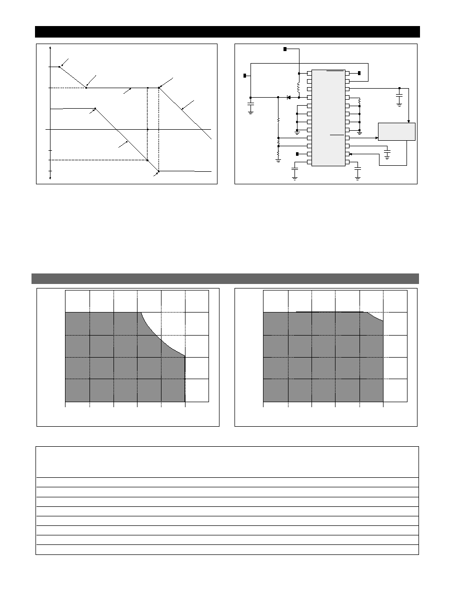
Figure 10. Bode plot of error amplifier (OTA) gain and modulator gain
added to the feedback resistor divider attenuation.
A pole at point C:
f
p
= 1/(R
4
C
2
),
(8g)
offsets the zero set by the ESR of the output capacitors.
An alternative scheme uses a single capacitor as shown in
Figure 11, to roll the gain off at a relatively low frequency.
Figure 11. A typical application diagram with external components con-
figured in a boost topology.
Step 9
Finally the watchdog timer period and Power on Reset
time is determined by:
t
Delay
= 1.353 ◊ C
Delay
R
BIAS
.
(9)
V
IN
NC
NC
V
SW
Gnd
Gnd
Gnd
Gnd
V
FB1
V
FB2
SELECT
COMP
V
REG
V
LIN
I
BIAS
Gnd
Gnd
Gnd
Gnd
C
Delay
WDI
C
OSC
R
BIAS
= 64.9k
100
µ
F
ESR<8
0.1
µ
F
C
COMP
0.33
µ
F
L=33
µ
H
V
IN
C
OUT
88
µ
F
(2)
100k
946
7.5k
R
1
R
2
R
3
C
delay
390pF
C
OSC
CS-51
1
1
RESET
ENABLE
(1)
V
OUT
= 18V, Select > 2V
V
OUT
= 16V, Select < 0.8V
MICROPROCESSOR
5V
Pole due to error amplifier
output impedance and C
1
G
0
f
z
= 1/2
R4C1
+G
B
A
C
f
P
= 1/
R
Load
C
OUT
error amplifier gain
f
CO
f
z
= 1/2
ESR C
OUT
f
P
= 1/
R
4
C
2
-20dB/dec
-G
Gain (dB)
modulator gain + feedback resistor divider attenuation
9
CS5111
Application Notes: continued
25
0
0
5
V
REG
(V)
50
75
100
10
20
25
I
LIN
(mA)
15
30
JA
= 35
∞
C/W
V
IN
= 14V
Max Total Power = 1.86W
25
0
0
5
V
REG
(V)
50
75
100
10
20
25
I
LIN
(mA)
15
30
JA
= 55
∞
C/W
V
IN
= 14V
Max Total Power = 1.18W
Worst Case Switcher
Worst Case Switcher
Linear Power
Power Available
Power Available
V
REG
V
IN
I
LIN
Dissipation
(
JA
= 55∞C/W)
(
JA
= 35∞C/W)
(V)
(V)
(mA)
(W)
(W)
(W)
20
14
25
0.44
0.74
1.42
20
14
50
0.83
0.35
1.03
20
14
75
1.22
*
0.64
20
14
100
1.60
*
0.26
25
14
25
0.60
0.58
1.26
25
14
50
1.11
0.07
0.75
25
14
75
1.62
*
0.24
25
14
100
2.14
*
*
Linear Regulator Output Current vs. Input Voltage
Figure 12: The shaded area shows the safe operating area of the CS5111 as a function of I
LIN
, V
REG
, and
JA
. Refer to the table below for typical
loads and voltages.
* Subjecting the CS5111 to these conditions will exceed the maximum total power that the part can handle, thereby forcing it into thermal limit.
Part Number
Description
CS5111YDWF24
24 Lead SO Wide
(internally fused leads)
CS5111YDWFR24
24 Lead SO Wide
(internally fused leads) (tape & reel)
10
Rev. 12/28/98
Thermal Data
24 Lead SO Wide
R
JC
typ
9
∞C/W
R
JA
typ
55
∞C/W
Package Specification
PACKAGE THERMAL DATA
Ordering Information
D
Lead Count
Metric
English
Max
Min
Max
Min
24 Lead SO Wide
15.60
15.20
.614 .598
(internally fused leads)
PACKAGE DIMENSIONS IN mm (INCHES)
CS5111
© 1999 Cherry Semiconductor Corporation
Cherry Semiconductor Corporation reserves the right to
make changes to the specifications without notice. Please
contact Cherry Semiconductor Corporation for the latest
available information.
1.27 (.050) BSC
7.60 (.299)
7.40 (.291)
10.65 (.419)
10.00 (.394)
D
0.32 (.013)
0.23 (.009)
1.27 (.050)
0.40 (.016)
REF: JEDEC MS-013
2.49 (.098)
2.24 (.088)
0.51 (.020)
0.33 (.013)
2.65 (.104)
2.35 (.093)
0.30 (.012)
0.10 (.004)
Surface Mount Wide Body (DW); 300 mil wide