1
Features
s
Linear Regulator
5V ± 2% @ 100mA
s
Switching Regulator
1.4A Peak Internal
Switch
120kHz Maximum
Switching Frequency
5V to 26V Operating
Supply Range
s
Smart Functions
Watchdog
s
Protection
Overtemperature
Current Limit
ENABLE
RESET
Package Options
24 Lead SO Wide
(Internally Fused Leads)
CS5112
1.4A Switching Regulator with 5V, 100mA Linear
Regulator with Watchdog, RESET and ENABLE
1
V
REG
V
LIN
I
BIAS
Gnd
Gnd
Gnd
Gnd
RESET
C
Delay
WDI
C
OSC
V
IN
NC
NC
V
SW
Gnd
Gnd
Gnd
Gnd
V
FB1
V
FB2
SELECT
COMP
ENABLE
CS5112
Description
Over
Temperature
V
IN
Linear
Error Amplifier
1.25V
V
REG
1.4A
V
SW
COMP
V
FB1
V
FB2
SELECT
V
LIN
I
BIAS
C
DELAY
RESET &
Watchdog Timer
Current
Limit
WDI
C
OSC
Base
Drive
RESET
Gnd
Bandgap
Reference
Oscillator
Multiplexer
+
-
COMP
Logic
+
-
+
-
+
-
Switcher Shutdown
Switcher
Error Amplifier
Current Sense Amplifier
ENABLE
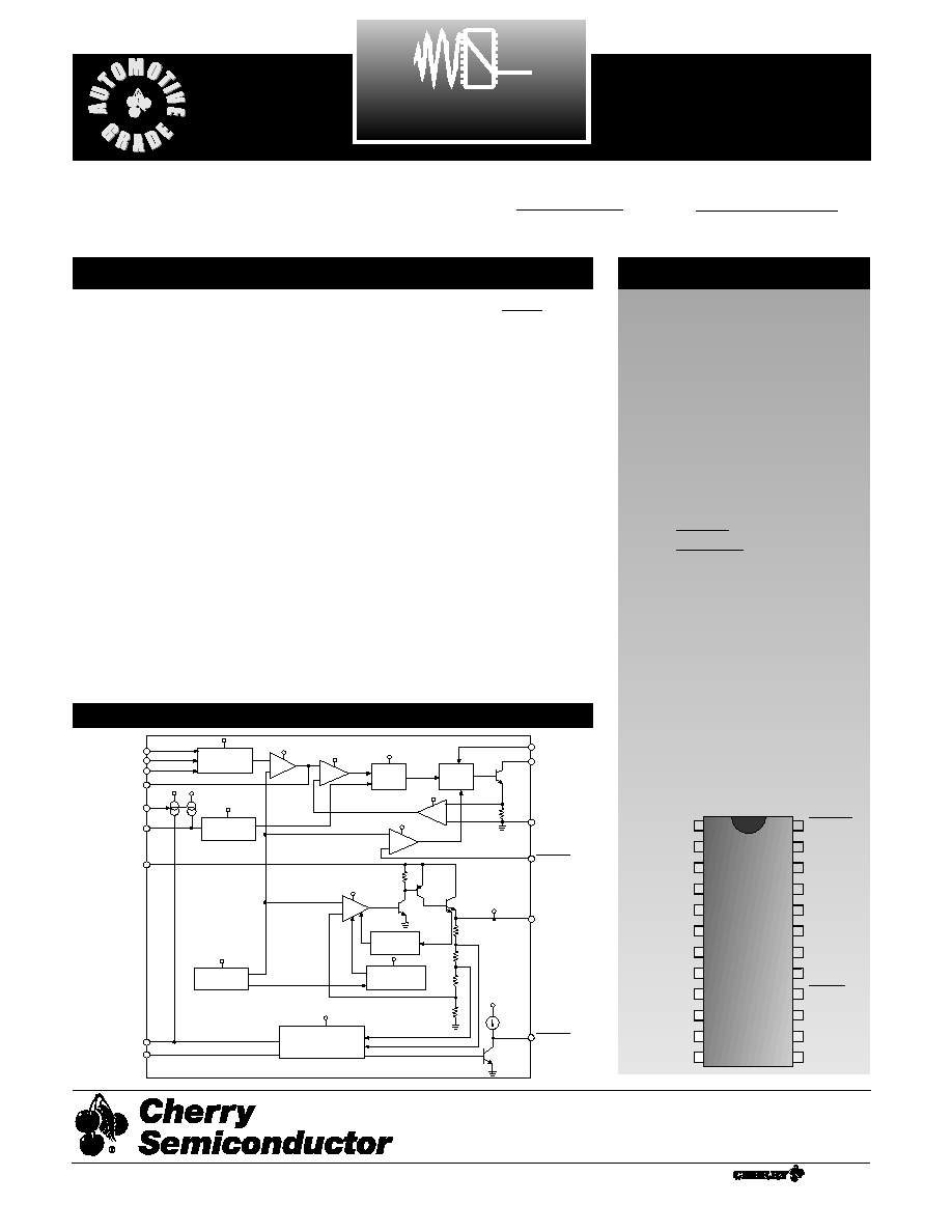
Block Diagram
A Company
®
Rev. 4/22/99
Cherry Semiconductor Corporation
2000 South County Trail, East Greenwich, RI 02818
Tel: (401)885-3600 Fax: (401)885-5786
Email: info@cherry-semi.com
Web Site: www.cherry-semi.com
The CS5112 is a dual output power sup-
ply integrated circuit. It contains a 5V
±2%, 100mA linear regulator, a watchdog
timer, a linear output voltage monitor to
provide a Power On Reset (POR) and a
1.4A current mode PWM switching reg-
ulator.
The 5V linear regulator is comprised of
an error amplifier, reference, and super-
visory functions. It has low internal sup-
ply current consumption and provides
1.2V (typical) dropout voltage at maxi-
mum load current.
The watchdog timer circuitry monitors
an input signal (WDI) from the micro-
processor. It responds to the falling
edge of this watchdog signal. If a correct
watchdog signal is not received within
the externally programmable time, a
reset signal is issued.
The externally programmable active
reset circuit operates correctly for an out-
put voltage (V
LIN
) as low as 1V. During
power up, or if the output voltage shifts
below the regulation limit,
tog-
gles low and remains low for the duration
of the delay after proper output voltage
regulation is restored. Additionally a reset
pulse is issued if the correct watchdog is
not received within the programmed
time. Reset pulses continue until the cor-
rect watchdog signal is received. The
reset pulse width and frequency, as well
as the Power On Reset delay, are set by
one external RC network.
The current mode PWM switching regu-
lator is comprised of an error amplifier
with selectable feedback inputs, a cur-
rent sense amplifier, an adjustable oscil-
lator, and a 1.4A output power switch
with anti-saturation control. The switch-
ing regulator can be configured in a
variety of topologies.
The CS5112 is load dump capable and
has protection circuitry which includes
current limit on the linear and switcher
outputs, and an overtemperature limiter.
RESET
2
CS5112
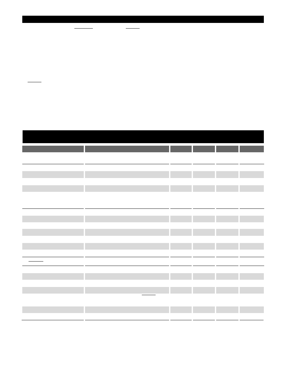
PARAMETER
TEST CONDITIONS
MIN
TYP
MAX
UNIT
Absolute Maximum Ratings
Logic Inputs/Outputs (
, SELECT, WDI,
) ................................................................................-0.3V to V
LIN
V
LIN
................................................................................................................................................................................-0.3V to 10V
V
IN
, V
REG:
DC Input Voltage .................................................................................................................................................-0.3V to 26V
Peak Transient Voltage (26V Load Dump @ 14V V
IN
)....................................................................................-0.3V to 40V
V
SW
Peak Transient Voltage .....................................................................................................................................................54V
C
OSC
, C
Delay
, COMP,V
FB1
, V
FB2
..................................................................................................................................-0.3V to V
LIN
Power Dissipation.............................................................................................................................................Internally Limited
V
LIN
Output Current ........................................................................................................................................Internally Limited
V
SW
Output Current .........................................................................................................................................Internally Limited
Output Sink Current ..................................................................................................................................................5mA
ESD Susceptibility (Human Body Model)..............................................................................................................................2kV
ESD Susceptibility (Machine Model).....................................................................................................................................200V
Storage Temperature ...................................................................................................................................................-65 to 150°C
Lead Temperature Soldering: Reflow (SMD styles only) ..........................................60 sec. max above 183°C, 230°C peak
RESET
RESET
ENABLE
Electrical Characteristics: 5V ≤ V
IN
≤ 26V and -40°C ≤ T
J
≤ 150°C, -40°C ≤ T
A
≤ 85°C, C
OUT
= 100µF (ESR≤8Ω),
C
Delay
= 0.1µF, R
BIAS
= 64.9kΩ, C
OSC
= 390 pF, C
COMP
= 0.1µF; unless otherwise specified.
s General
I
IN
Off Current
6.6V ≤ V
IN
≤ 26V, I
SW
= 0A
2.0
mA
I
IN
On Current
6.6V ≤ V
IN
≤ 26V, I
SW
= 1.4A
30
70
mA
I
REG
Current
I
LIN
= 100mA, 6.6V ≤ V
REG
≤ 26V
6
mA
Thermal Limit
Guaranteed by design
160
210
°C
s 5V Regulator Section
V
LIN
Output Voltage
6.6V ≤ V
REG
≤ 26V, 1mA ≤ I
LIN
≤ 100mA
4.9
5.0
5.1
V
Dropout Voltage
(V
REG
- V
LIN
) @ I
LIN
= 100mA
1.2
1.5
V
Line Regulation
6.6V ≤ V
REG
≤ 26V, I
LIN
= 5mA
5
25
mV
Load Regulation
V
REG
= 19V, 1mA ≤ I
LIN
≤ 100mA
5
25
mV
Current Limit
6.6V ≤ V
REG
≤ 26V
120
mA
DC Ripple Rejection
14V ≤ V
REG
≤ 24V
60
75
dB
s
Section
Low Threshold (V
RTL
)
V
LIN
Decreasing
4.05
4.25
4.45
V
High Threshold (V
RTH
)
V
LIN
Increasing
4.20
4.45
4.70
V
Hysteresis
V
RTH
- V
RTL
140
190
240
mV
Active High
V
LIN
> V
RTH
, I
RESET
= -25µA
V
LIN
- 0.5
V
Active Low
V
LIN
= 1V, 10kΩ pullup from
to V
LIN
0.4
V
V
LIN
= 4V, I
RESET
= 1mA
0.7
V
Delay Invalid
WDI
6.25
8.78
11.0
ms
Power On Delay
V
LIN
crossing V
RTH
6.25
ms
RESET
RESET

3
PARAMETER
TEST CONDITIONS
MIN
TYP
MAX
UNIT
CS5112
s Watchdog Input (WDI)
VIH
Peak WDI needed to activate
2.0
V
VIL
0.8
V
Hysteresis
Note 1
25
50
mV
Pull-Up Resistor
WDI=0V
20
50
100
kΩ
Low Threshold
6.25
8.78
11.0
ms
Floating Input Voltage
3.5
V
WDI Pulse Width
5
µs
s Switcher Section
Minimum Operating
5.0
V
Input Voltage
Switching Frequency
Refer to Figure 1d.
80
95
110
kHz
Switch Saturation Voltage
I
SW
= 1.4A
0.7
1.1
1.6
V
Output Current Limit
1.4
2.5
A
Max Switching Frequency
V
SW
= 7.5V with 50Ω load,
120
kHz
Refer to Figure 1d.
V
FB1
Regulation Voltage
1.206
1.25
1.294
V
V
FB2
Regulation Voltage
1.206
1.25
1.294
V
V
FB1
, V
FB2
Input Current
V
FB1
= V
FB2
= 5V
1
µA
Oscillator Charge Current
C
OSC
= 0V
35
40
45
µA
Oscillator Discharge Current
C
OSC
= 4V
270
320
370
µA
C
Delay
Charge Current
C
Delay
= 0V
35
40
45
µA
Switcher Max Duty Cycle
V
SW
= 5V with 50Ω load,
72
85
95
%
V
FB1
= V
FB2
= 1V
Current Sense Amp Gain
I
SW
= 2.3A
7
Error Amp DC Gain
67
dB
Error Amp Transconductance
2700
µA/V
s
Input
VIL
0.8
1.24
V
VIH
1.30
2.0
V
Hysteresis
60
mV
Input Impedance
10
20
40
kΩ
s Select Input
VIL (Selects V
FB1
)
4.9 ≤ V
LIN
≤ 5.1
0.8
1.25
V
VIH (Selects V
FB2
)
4.9 ≤ V
LIN
≤ 5.1
1.25
2.0
V
SELECT Pull-Up
SELECT = 0V
10
24
50
kΩ
Floating Input Voltage
3.5
4.5
V
Note 1: Guaranteed by Design, not 100% tested in production.
ENABLE
RESET
Electrical Characteristics: 5V ≤ V
IN
≤ 26V and -40°C ≤ T
J
≤ 150°C, -40°C ≤ T
A
≤ 85°C, C
OUT
= 100µF (ESR≤8Ω),
C
Delay
= 0.1µF, R
BIAS
= 64.9kΩ, C
OSC
= 390 pF, C
COMP
= 0.1µF; unless otherwise specified.

4
Typical Performance Characteristics
0A
20mA
40mA
60mA
80mA
100mA
3.5mA
4.0mA
4.5mA
I
LIN
I
REG
- I
LIN
-30mA
-40mA
0A
0.5A
I
SW
-20mA
-10mA
0A
1.0A
1.5A
2.0A
I
IN
ISW
0A
0.5A
1.0A
1.5A
2.0A
0.4V
0.0V
0.6V
0.8V
1.2V
1.0V
V
SW
0.2V
1.4V
Package Lead Description
PACKAGE LEAD #
LEAD SYMBOL
FUNCTION
CS5112
40
0
0
C
OSC
(pF)
80
120
160
1000
Frequency (kHz)
20
60
100
140
2000
3000
500
1500
2500
180
Figure 1a. 5V Regulator Bias Current vs. Load Current.
Figure 1b. Supply Current vs. Switch Current.
Figure 1c. Switch Saturation Voltage.
Figure 1d. Oscillator Frequency (kHz) vs. C
OSC
(pF), assuming R
BIAS
=
64.9kΩ.
24 Lead SO Wide
1
V
IN
Supply Voltage.
2, 3
NC
No connection.
4
V
SW
Collector of NPN power switch for switching regulator section.
5,6,7,8,17,18,19,20
Gnd
Connected to the heat removing leads.
9
V
FB1
Feedback input voltage 1 (referenced to 1.25V)
10
V
FB2
Feedback input voltage 2 (referenced to 1.25V)
11
SELECT
Logic level input that selects either V
FB1
or V
FB2
. An open selects
V
FB2
. Connect to Gnd to select V
FB1
.
12
COMP
Output of the transconductance error amplifier.
13
C
OSC
A capacitor connected to Gnd sets the switching frequency.
Refer to Figure 1d.
14
WDI
Watchdog input. Active on falling edge.
15
C
Delay
A capacitor connected to Gnd sets the Power On Reset and
Watchdog time.
16
output. Active low if V
LIN
is below the regulation limit.
If watchdog timeout is reached, a reset pulse train is issued.
21
I
BIAS
A resistor connected to Gnd sets internal bias currents as well as
the C
OSC
and C
Delay
charge currents.
22
V
LIN
Regulated 5V output from the linear regulator section.
23
V
REG
Input voltage to the linear regulator and the internal supply cir-
cuitry.
24
Logic level input to shut down the switching regulator.
ENABLE
RESET
RESET
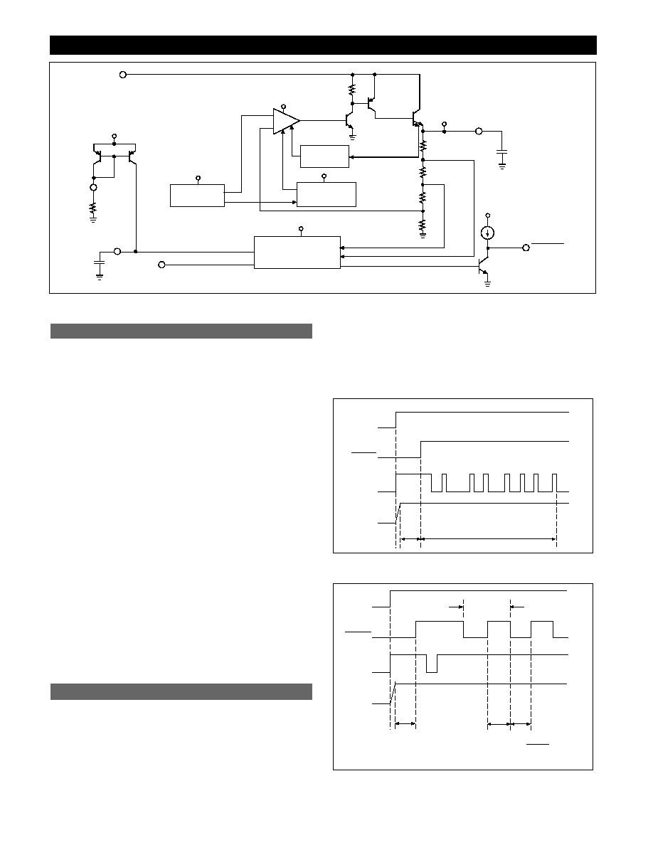
Circuit Description
CS5112
5
The 5V linear regulator consists of an error amplifier,
bandgap voltage reference, and a composite pass transistor.
The 5V linear regulator circuitry is shown in Figure 2.
When an unregulated voltage greater than 6.6V is applied
to the V
REG
input, a 5V regulated DC voltage will be pre-
sent at V
LIN
. For proper operation of the 5V linear regula-
tor, the I
BIAS
lead must have a 64.9kΩ pull down resistor to
ground. A 100µF or larger capacitor with an ESR <8Ω
must be connected between V
LIN
and ground. To operate
the 5V linear regulator as an independent regulator (i.e.
separate from the switching supply), the input voltage
must be tied to the V
REG
lead.
As the voltage at the V
REG
input is increased, Q
1
is turned
on. Q
1
provides base drive for Q
2
which in turn provides
base current for Q
3
. As Q
3
is turned on, the output voltage,
V
LIN
, begins to rise as Q
3
’s output current charges the out-
put capacitor, C
OUT
. Once V
LIN
rises to a certain level, the
error amplifier becomes biased and provides the appropri-
ate amount of base current to Q
1
. The error amplifier mon-
itors the scaled output voltage via an internal voltage
divider, R
2
through R
5
, and compares it to the bandgap
voltage reference. The error amplifier output or error sig-
nal is an output current equal to the error amplifier’s input
differential voltage times the transconductance of the
amplifier. Therefore, the error amplifier varies the base
current to Q
1
, which provides bias to Q
2
and Q
3
, based on
the difference between the reference voltage and the
scaled V
LIN
output voltage.
The watchdog timer circuitry monitors an input signal
(WDI) from the microprocessor. It responds to the falling
edge of this watchdog signal which it expects to see within
an externally programmable time (see Figure 3).
The watchdog time is given by:
t
WDI
= 1.353
¥ C
Delay
R
BIAS
Using C
Delay
= 0.1µF and R
BIAS
= 64.9kΩ gives a time rang-
ing from 6.25ms to 11ms assuming ideal components. Based
on this, the software must be written so that the watchdog
arrives at least every 6.25ms. In practice, the tolerance of
C
Delay
and R
BIAS
must be taken into account when calculat-
ing the minimum watchdog time (t
WDI
).
Figure 3. Timing diagram for normal regulator operation.
Figure 4. Timing diagram when WDI fails to appear within the preset
time interval, t
WDI
.
V
LIN
WDI
RESET
V
REG
t
POR
A
B
A: Watchdog waiting for
low-going transition on
WDI
50% Duty
Cycle
B: RESET stays low for
t
WDI
time.
V
LIN
WDI
RESET
V
REG
t
POR
Normal Operation
Control Functions
5V Linear Regulator
Over
Temperature
Linear
Error
Amplifier
1.25V
V
REG
V
LIN
C
delay
RESET &
Watchdog Timer
Current
Limit
WDI
RESET
Bandgap
Reference
+
-
I
BIAS
R
BIAS
64.9k
W
R
1
R
2
R
3
R
4
R
5
C
OUT
= 100
mF
ESR < 8
W
Q
1
Q
2
Q
3
Figure 2. Block diagram of 5V linear regulator portion of the CS5112.