V
CC
BIAS
UVLO
SS
Gnd
GATE
IS
V
FB
R8
0.39
Q2
IRFR220
R5
17.4k
C2
1.5
µ
F,
100V
C1
0.1
µ
F,
100V
R2
200k
10
µ
H
36-75VIN
L1
R1
510k
Q1
ZVN3310A
T1
D1
MBRD360CT
R3
47
R6
1k
C3
.022
µ
F
C6
.01
µ
F
R7
30.1k
C5
47
µ
F,
10V
ISOLATED
RTN
5VOUT
ENABLE
48VRTN
D4
R4
10
BAS16LT1
C4
0.47
µ
F,
25V
C8
1000pF
C7
0.1
µ
F
TPS5908
U2
R9
10.0k
C9
1000pF
CS5124
CTX15-14514
Features
s
Line UVLO Monitoring
s
Low Current Sense
Voltage for Resistive
Current Sensing
s
External Synchronization
to Higher or Lower
Frequency Oscillator
(CS5126 Only)
s
Bias for Start up Circuitry
(CS5124 Only)
s
Thermal Shutdown
s
Sleep On/Off Pin
s
Soft Start Timer
s
Leading Edge Blanking
s
Direct Optocoupler
Interface
s
90ns Propagation Delay
s
35ns Driver Rise and Fall
Times
s
Sleep Mode
Package Options
CS5124/6
High Performance, Integrated Current Mode
PWM Controllers
CS5124/6
Description
Applications Diagram
8 Lead SO Narrow
1
1
V
CC
BIAS
UVLO
SS
Gnd
GATE
I
SENSE
V
FB
Cherry Semiconductor Corporation
2000 South County Trail, East Greenwich, RI 02818
Tel: (401)885-3600 Fax: (401)885-5786
Email: info@cherry-semi.com
Web Site: www.cherry-semi.com
A Company
Æ
Rev. 3/12/99
Gnd
UVLO
1
V
CC
SYNC
SS
GATE
I
SENSE
V
FB
CS5124
CS5126
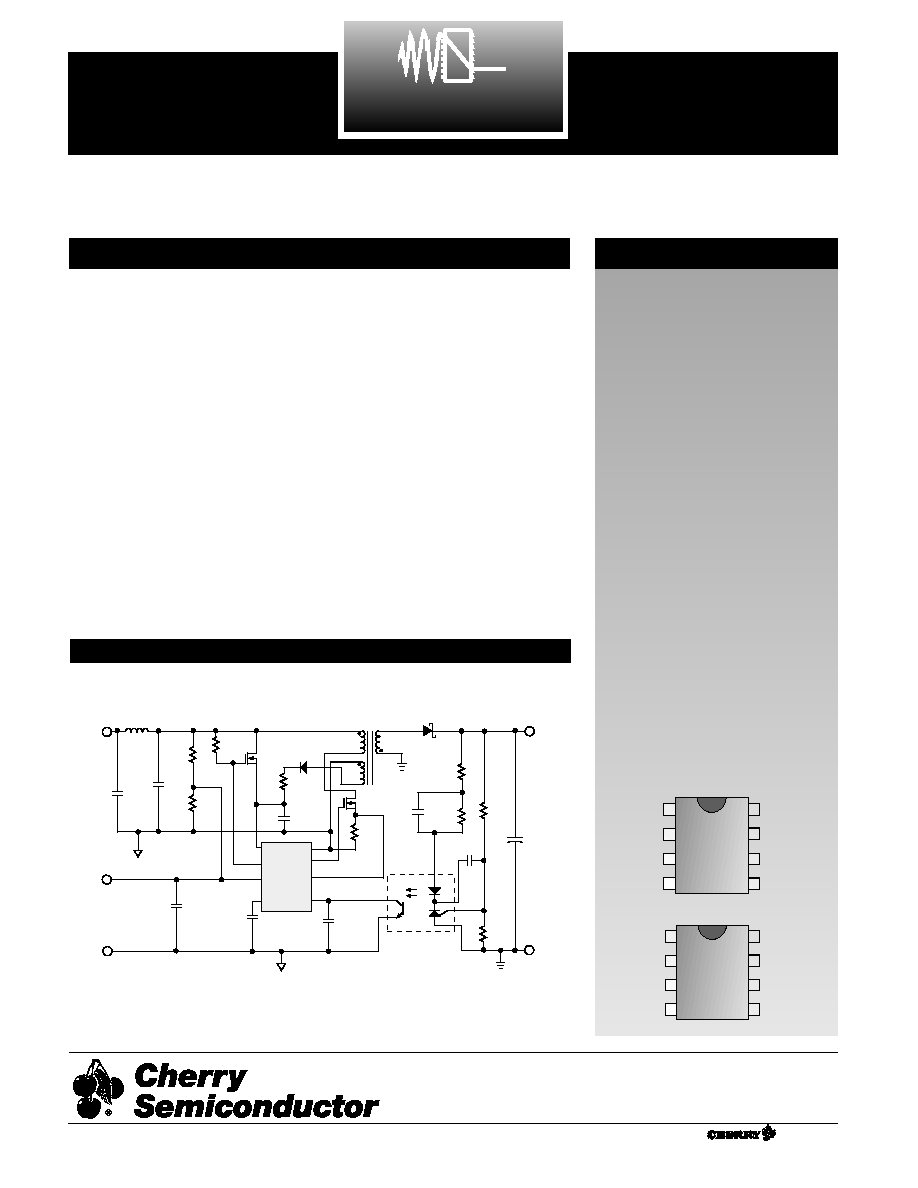
48V to 5V, 1A flyback converter using the CS5124
The CS5124/6 is a fixed frequency
current mode controller designed
specifically for DC-DC converters
found in the telecommunications
industry. The CS5124/6 integrates
many commonly required current
mode power supply features and
allows the power supply designer to
realize substantial cost and board
space savings. The product matrix is
as follows:
CS5124: 400kHz w/V
BIAS
Pin,
195mV first current sense threshold
CS5126: 200kHz w/SYNC Pin,
335mV first current sense threshold
The CS5124/6 integrates the follow-
ing features: Internal Oscillator, Slope
Compensation, Sleep On/Off, Under
Voltage Lock Out, Thermal
Shutdown, Soft Start Timer, Low
Voltage Current Sense for Resistive
Sensing, Second Current Threshold
for Pulse by Pulse Over Current
Protection, a Direct Optocoupler
Interface and Leading Edge Current
Blanking.
The CS5124/6 has supply range of
7.7V to 20V and is available in 8 pin
SO narrow package.

Pin Symbol
Lead Name
V
MAX
V
MIN
I
SOURCE
I
SINK
V
CC
V
CC
Power Input
20V
-0.3V
1mA
1.5A Peak
200mA DC
SYNC (CS5126)
Clock Synchronization Input
20V
-0.3V
1mA
1mA
V
BIAS
(CS5124)
V
CC
Clamp Output
20V
-0.3V
1mA
1mA
UVLO
UVLO Shutdown Input
6V
-0.3V
1mA
1mA
SS
Soft Start Capacitor Input
6V
-0.3V
1mA
2mA
V
FB
Voltage Feed Back Input
6V
-0.3V
3mA
20mA
I
SENSE
Current Sense Input
6V
-0.3V
1mA
1mA
GROUND
Ground 0V
0V
1.5A
peak
1mA
200mA DC
GATE
Gate Drive Output
20V
-0.3V
1.5A Peak
1.5A Peak
200mA DC
200mA DC
Operating Junction Temperature, T
J
. . . . . . . . . . . . . . . . . . . . . . . . . . . . . . . . . . . . . . . . . . . . . . . . . . . . . . . . . . . . . . .-40 to 135∞C
Storage Temperature Range, T
S
. . . . . . . . . . . . . . . . . . . . . . . . . . . . . . . . . . . . . . . . . . . . . . . . . . . . . . . . . . . . . . . . . . .-40 to 150∞C
ESD (Human Body Model) . . . . . . . . . . . . . . . . . . . . . . . . . . . . . . . . . . . . . . . . . . . . . . . . . . . . . . . . . . . . . . . . . . . . . . . . . . . . . .2kV
ESD (Machine Model) . . . . . . . . . . . . . . . . . . . . . . . . . . . . . . . . . . . . . . . . . . . . . . . . . . . . . . . . . . . . . . . . . . . . . . . . . . . . . . . . .200V
Lead Temperature Soldering:
Reflow (SMD styles only) . . . . . . . . . . . . . . . . . . . . . . . . . . . . . . . . . . . . . . . . . . . . . . . . . .60 sec. max above 183∞C, 230∞C peak
CS5124/6
2
Absolute Maximum Ratings
PARAMETER
TEST CONDITIONS
MIN
TYP
MAX
UNIT
Electrical Characteristics: -40∞C T
J
125∞C, -40∞C T
A
105∞C, 7.60V V
CC
20V, UVLO = 3.0V, I
SENSE
= 0V,
C
V(CC)
= 0.33µF, C
GATE
= 1nF (ESR = 10), C
SS
= 470pF C
V(FB)
= 100pF
,
unless otherwise stated.
s
General
I
CC
Operating - V
GATE
not switching.
10
13
mA
I
CC
at V
CC
Low
V
CC
= 6V
500
750
µA
I
CC
Sleep
V
UVL
= 1V
210
275
µA
s
Low V
CC
Lockout
V
CC
Turn-on Threshold Voltage
7.2
7.7
8.3
V
V
CC
Turn-off Threshold Voltage
6.8
7.3
7.8
V
V
CC
Hysteresis
350
425
500
mV
s
UVLO
Sleep Threshold Voltage
UVLO decreasing
1.5
1.8
2.3
V
Sleep Threshold Voltage
UVLO increasing
1.88
2.45
V
Sleep Hysteresis
35
85
150
mV
UVLO Turn-off
(Note 1)
2.3
2.45
2.6
V
Threshold Voltage
UVLO Turn-on
(Note 1)
2.50
2.63
2.76
V
Threshold Voltage
UVLO Hysteresis
Turn-on ≠ Turnoff (-40∞C T
J
100∞C)
170
185
200
mV
(Note 1)
UVLO Hysteresis
Turn-on ≠ Turnoff (100∞C T
J
125∞C)
50
185
400
mV
(Note 1)
UVLO Input Bias Current
-1
1
µA
UVLO Clamp
With UVLO sinking 1mA.
5
7.5
12
V

CS5124/6
3
Electrical Characteristics: -40∞C T
J
125∞C, -40∞C T
A
105∞C, 7.60V V
CC
20V, UVLO = 3.0V, I
SENSE
= 0V,
C
V(CC)
= 0.33µF, C
GATE
= 1nF (ESR = 10), C
SS
= 470pF C
V(FB)
= 100pF
,
unless otherwise stated.
PARAMETER
TEST CONDITIONS
MIN
TYP
MAX
UNIT
s
V
CC
Clamp and BIAS Pin
CS5124 Only. Connect an NFET as follows: BIAS = G, V
CC
= S, V
IN
= D.
V
CC
Clamp Voltage
36V V
IN
60V, 220nF
7.275
7.9
8.625
V
C
SS
500nF, R = 500k
BIAS Minimum Voltage
Measure Voltage on BIAS with:
1.6
2.8
4
V
10V V
CC
20V and 50µA I
BIAS
1mA
BIAS Clamp
With BIAS pin sinking 1mA
12
15
20
V
s
200kHz Oscillator
CS5126 Only
Operating Frequency
175
200
225
kHz
Max Duty Cycle Clamp
78
82.5
85
%
Slope Compensation
12
18
23
mV/µs
(Normal operation)
Slope Compensation
(Synchronized operation)
(Note 1)
7
12
16
mV/µs
SYNC Input Threshold Voltage
1
2
3
V
SYNC Input Impedance
Measured with SYNC = 1V &10V
50
120
230
k
s
400kHz Oscillator
CS5124 Only
Operating Frequency
360
400
440
kHz
Max Duty Cycle Clamp
80.0
82.5
85.0
%
Slope Compensation
15
21
26
mV/µs
s
Soft Start
Soft Start Charge Current
7
10
13
µA
Soft Start Discharge Current
0.5
10.0
mA
V
SS
Voltage when V
FB
V
FB
= 300mV
1.40
1.62
1.80
V
Begins to Rise
Peak Soft Start Charge Voltage
4.7
4.9
V
Valley Soft Start Discharge Voltage
200
275
400
mV
s
Current Sense
CS5124 Only
First Current Sense Threshold
At max duty cycle.
170
195
215
mV
Second Current Sense Threshold
250
275
315
mV
I
SENSE
to GATE Prop. Delay
0 to 700mV pulse into I
SENSE
60
90
130
ns
(after blanking time)
Leading Edge Blanking Time
0 to 400mV pulse into I
SENSE
90
130
180
ns
Internal Offset
(Note 1)
60
mV
s
Current Sense
CS5126 Only
First Current Sense Threshold
At max duty cycle
300
335
360
mV
Second Current Sense
485
525
575
mV
Threshold
I
SENSE
to GATE Prop. Delay
0 to 800mV pulse into I
SENSE
60
90
130
ns
(after blanking time)
Leading Edge Blanking Time
0 to 550mV pulse into I
SENSE
110
175
210
ns
Internal Offset
(Note 1)
125
mV

Package Lead Description
PACKAGE LEAD #
LEAD SYMBOL
FUNCTION
CS5124/6
4
Electrical Characteristics: -40∞C T
J
125∞C, -40∞C T
A
105∞C, 7.60V V
CC
20V, UVLO = 3.0V, I
SENSE
= 0V,
C
V(CC)
= 0.33µF, C
GATE
= 1nF (ESR = 10), C
SS
= 470pF C
V(FB)
= 100pF
,
unless otherwise stated.
PARAMETER
TEST CONDITIONS
MIN
TYP
MAX
UNIT
8 Lead SO Narrow
CS5124
CS5126
1
1
V
CC
V
CC
Power Input Pin.
2
-
BIAS
V
CC
Clamp Output Pin. This pin will control the gate of an N-channel MOS-
FET that in turn regulates V
CC
. This pin is internally clamped at 15V when
the IC is in sleep mode.
-
3
SYNC
Clock Synchronization Pin. A positive edge will terminate the current PWM
cycle. Ground this pin when it is not used.
3
2
UVLO
Sleep and under voltage lockout pin. A voltage greater than 1.8V causes the
chip to "wake up" however the GATE remains low. A voltage greater than
2.6V on this pin allows the output to switch.
4
4
SS
Soft Start Capacitor Pin. A capacitor placed between SS and GROUND is
charged with 10µA and discharged with 10mA. The Soft Start capacitor con-
trols both soft-start time and hiccup mode frequency.
5
5
V
FB
Voltage Feedback Pin. The collector of an optocoupler is typically tied to this
pin. This pin is pulled up internally by a 4.3k resistor to 5V and is clamped
internally at 2.9V(2.65V). If V
FB
is pulled > 4V, the oscillator is disabled and
GATE will stay high. If the V
FB
pin is pulled < 0.49V, GATE will stay low.
6
6
I
SENSE
Current Sense Pin. This pin is connected to the current sense resistor on the
primary side. If V
FB
is floating, the GATE will go low if I
SENSE
= 195mV
(335mV). If I
SENSE
> 275mV (525mV), Soft Start will be initiated.
7
7
GATE
Gate Drive Output Pin. Capable of driving a 3nF load. GATE is nominally
clamped to 13.5V.
8
8
Gnd
Ground Pin.
s
Voltage Feedback
V
FB
Pull-up Res.
2.9
4.3
8.1
k
V
FB
Clamp Voltage
CS5124 Only
2.63
2.90
3.15
V
V
FB
Clamp Voltage
CS5126 Only
2.40
2.65
2.90
V
V
FB
Fault Voltage Threshold
460
490
520
mV
s
Output Gate Drive
Maximum Sleep
V
CC
= 6.0V, I
OUT
= 1mA
1.2
2.0
V
Pull-down Voltage
GATE High (AC)
Series resistance < 1 (Note 1)
V
CC
-1
V
CC
-0.5
V
GATE Low (AC)
Series resistance < 1 (Note 1)
0.0
0.5
V
GATE High Clamp Voltage
V
CC
= 20V
11.0
13.5
16.0
V
Rise Time
Measure GATE rise time,
45
65
ns
1V < GATE < 9V; V
CC
=12V
Fall Time
Measure GATE fall time,
25
55
ns
9V > GATE > 1V; V
CC
= 12V
s
Thermal Shutdown
Thermal Shutdown Temperature (Note 1) (GATE low)
135
150
165
∞C
Thermal Enable Temperature
(Note 1) (GATE switching)
100
125
150
∞C
Thermal Hysteresis
(Note 1)
15
25
35
∞C
Notes
1. Not tested in production. Specification is guaranteed by design.

CS5124/6
5
Block Diagram
G2
{2.65V}
2.90V
V5
REF
GATE
˜
V
FB
I
SENSE
V
CC
2.62 V/2.45V
1.91 V/1.83V
REMOTE
(SLEEP) COMP
SS
V
CC
UVLO COMP
7.7 V/7.275V
+
-
LINE AMP
(CS5124 ONLY)
2.9 R
R
2.0V
+
+
-
SS COMP
275mV
V
V
V
V
1.32V
+
V
{525mV}
275mV
{125mV}
60mV
V
+
+
DRIVER
+
-
+
-
490mV
V
FB
COMP
PWM COMP
2ND I
COMP
+
-
+
LINE UVLO COMP
RESET DOMAIN
G6
4500
BIAS
UVLO
G1
V5
REF
F1
R
Q
S
G7
1000
BLANKING
10
µ
A
V5
REF
V5
REF
V
BLANK
V
CC
V
V
TSHUT
V
F2
R
Q
S
+
-
SS AMP
+
-
V
{85 mV/us}
170mV us
{1/5}
1/10
G5
OSC
RAMP
ENABLE
V
CC
V
REF
= 5V
G3
+
-
V
REFOK
SYNC
{CS5126 ONLY}
DIS
F3
R
Q
S
SET DOMAIN
SOFT START LATCH
150
∞
C/125
∞
C
+
Gnd
+
+
+
+
+
+
-
+
-
Theory of Operation
Powering the IC
V
CC
can be powered directly from a regulated supply
and requires 500µA of start-up current. The CS5124/6
includes a line bias pin (BIAS) that can be used to control a
series pass transistor for operation over a wide input volt-
age. The BIAS pin will control the gate voltage of an N-
channel MOSFET placed between V
IN
and V
CC
to regulate
V
CC
at 8V.
V
CC
and UVLO Pins
The UVLO pin has three different modes; low power shut-
down, Line UVLO, and normal operation. To illustrate
how the UVLO pin works; assume that V
IN
, as shown in
the application schematic, is ramped up starting at 0V with
the UVLO pin open. The SS and I
SENSE
pins also start at 0V.
While the UVLO is below 1.8V, the IC will remain in a low
current sleep mode and the BIAS pin of the CS5124 is inter-
nally clamped to a maximum of 15V. When the voltage on
the UVLO pin rises to between 1.8V and 2.6V the reference
for the V
CC
UVLO is enabled and V
CC
is regulated to 8V by
the BIAS pin (CS5124 only), but the IC remains in a UVLO
state and the output driver does not switch. When the
UVLO pin exceeds 2.6V and the V
CC
pin exceeds 7.7V, the
GATE pin is released from a low state and can begin
switching based on the comparison of the I
SENSE
and V
FB
pins. The Soft Start capacitor begins charging from 0V at
10µA. As the capacitor charges, a buffered version of the
capacitor voltage appears on the V
FB
pin and the V
FB
volt-
age begins to rise. As V
FB
rises the duty cycle increases
until the supply comes into regulation.
Soft Start
Soft Start is accomplished by clamping the V
FB
pin 1.32V
below the SS pin during normal start up and during restart
after a fault condition. When the CS5124/6 starts, the Soft
Start capacitor is charged from a 10µA source from 0V to
4.9V. The V
FB
pin follows the Soft Start pin offset by ≠1.32V
until the supply comes into regulation or until the Soft
Start error amp is clamped at 2.9V (2.65V for the CS5126).
During fault conditions the Soft Start capacitor is dis-
charged at 10mA.
Fault Conditions
The CS5124/6 recognizes the following faults: UVLO off,
Thermal Shutdown, V
REF(OK)
, and Second Current
Threshold. Once a fault is recognized, fault latch F2 is set
and the IC immediately shuts down the output driver and
discharges the Soft Start capacitor. Soft Start will begin
only after all faults have been removed and the Soft Start
capacitor has been discharged to less than 0.275V. Each
fault will be explained in the following sections.