
The CS5132 is a dual output CPU
power supply controller. It con-
tains a synchronous dual NFET
buck controller utilizing the V
2
TM
control method to achieve the
fastest possible transient response
and best overall regulation. The
CS5132 also contains a second non-
synchronous NFET buck con-
troller. These synchronous and
non-synchronous buck regulators
are designed to power the core and
I/O logic of the latest high perfor-
mance CPUs. The CS5132 incorpo-
rates many additional features
required to ensure the proper
operation and protection of the
CPU and power system. The
CS5132 dual output provides the
industry’s most highly integrated
solution, minimizing external com-
ponent count, total solution size,
and cost.
The CS5132 is specifically designed
to power Intel’s Pentium
®
II pro-
cessor and includes the following
features: 5 bit DAC and fixed
1.23V reference, Power-Good out-
put, hiccup mode overcurrent pro-
tection, adaptive voltage position-
ing, and overvoltage protection.
The CS5132 will operate over an
8.4V to 14V range and is available
in 24 lead surface mount package.
1
Features
+5V
+12V
+5V
+3.3V (V
I/O
)
V
CC(CORE)
V
ID0
V
ID1
V
ID3
V
ID2
V
ID4
GATE
Q3
PCB TRACE
(FreeCurrent
Sensing Element)
6.6m
W
L2
3.5
mH
MBRD835L
V
OUT2
10V
510
W
V
FFB2
2K
1%
1.18K
1%
V
FB2
C
OFF2
V
CC1
V
CC2
LGnd
GATE(H)
Q1
1.2
mH
L1
Q2
GATE(L)
COMP2
PCB TRACE (Free
Current Sensing
Element)
3.3m
W
10V
10V
510
W
V
FFB1
V
OUT1
PWRGD
OVP
COMP1
C
OFF1
PGnd
23
24
1
2
3
12
11
14
20
16
4
5
21
22
6
8
13
19
17
15
C1
C6-C11
C12
C14
C15
C16
C17
C18-C21
C23-C30
R1
R2
R3
R4
V
FB1
7
C3-C5
x 4
510
W
R5
510
W
R6
FS70VSJ-03
0.1
mF
0.1
mF
1200
mF
1200
mF x 6
1200
mF x 8
680pF
0.1
mF
D1
390pF
1
mF
1200
mF x 3
9
18
FS70VSJ-03
FS70VSJ-03
10
10V
10K
100pF
51
W
C13
0.1
mF
100
W
0.01
mF
10K
R10
C25
R9
R8
R7
C22
+12V
C2
1
mF
s
Synchronous Switching
Regulator Controller (V
CORE
)
s
Dual N-Channel MOSFET
Synchronous Buck Design
s
V
2
TM
Control Topology
s
200ns Transient Loop Response
s
5 bit DAC with 1% Tolerance
s
Hiccup Mode Overcurrent
Protection
s
65ns adaptive FET Non-Overlap
Time
s
Non-Synchronous Switching
Regulator Controller (V
I/O
)
s
Single N-Channel MOSFET
buck design
s
Adjustable Output with 2%
Tolerance
s
System Power Management
Pentium
®
II System V
CORE
and V
I/O
Controlled by
a Single IC
Power-Good Output
Monitors V
CORE
Switching
Regulator Output
OVP Signal Monitors V
CORE
Switching Regulator Output
Package Options
CS5132
Dual Output CPU Buck Controller
CS5132
Description
Application Diagram
16
15
14
13
12
11
10
1
2
3
4
5
6
7
8
V
ID2
V
ID3
V
ID4
C
OFF1
COMP1
V
OUT1
V
FB1
V
FFB1
V
ID1
V
ID0
PWRGD
OVP
V
CC1
GATEL
PGND
GATEH
LGND
V
CC2
9
17
18
V
FFB2
GATE
19
20
V
FB2
C
OFF2
V
OUT2
COMP2
21
22
23
24
24L SO Wide
5V/12V to 2V/16A for Pentium
®
II V
CC(CORE)
, 5V/12V to 3.3V/8A for V
I/O
Pentium is a registered trademark of Intel Corporation.
V
2
is a trademark of Switch Power, Inc.
Rev. 11/3/98
Cherry Semiconductor Corporation
2000 South County Trail, East Greenwich, RI 02818
Tel: (401)885-3600 Fax: (401)885-5786
Email: info@cherry-semi.com
Web Site: www.cherry-semi.com
A Company
®

2
CS5132
Package Pin Description
PACKAGE PIN #
PIN SYMBOL
FUNCTION
Absolute Maximum Ratings
Pin Symbol
Pin Name
V
MAX
V
MIN
I
SOURCE
I
SINK
V
CC1
IC Logic and Low Side Driver Power Input
16V
-0.3V
N/A
1.5A Peak
200mA DC
V
CC2
IC High Side Drivers Power Input
16V
-0.3V
N/A
3A Peak
400mA DC
COMP1, COMP2
Compensation Pins for the V
CORE
6V
-0.3V
1mA
5mA
and V
I/O
error amplifiers.
V
FB1
, V
OUT1
, V
ID0-4
, V
CORE
Voltage Feedback Input Pin,
V
OUT2
, V
FB2
, V
FFB1
, V
CORE
Output Voltage Sense Pin,
V
FFB2
Voltage ID DAC Input Pins, V
I/O
Output Voltage
6V
-0.3V
1mA
1mA
Sense Pin, V
I/O
Voltage Feedback Input Pin,
V
CORE
PWM comparator Fast Feedback Pin, V
I/O
PWM comparator Fast Feedback Pin.
C
OFF1
, C
OFF2
Off-Time Pins for the V
CORE
and V
I/O
regulators
6V
-0.3V
1mA
50mA
GATE(H), GATE
High-Side FET Drivers for the V
CORE
16V
-0.3V
1.5A Peak
1.5A Peak
and V
I/O
regulators.
200mA DC
200mA DC
GATE(L)
Low-Side FET Driver
16V
-0.3V
1.5A Peak
1.5A Peak
200mA DC
200mA DC
PWRGD
Power-Good Output
6V
-0.3V
1mA
30mA
OVP
Overvoltage Protection
15V
-0.3V
30mA
1mA
PGnd
Power Ground
0V
0V
3A Peak
N/A
400mA DC
LGnd
Logic Ground
0V
0V
40mA
N/A
23,24,1,2,3
V
IDO
– V
ID4
Voltage ID DAC inputs. These pins are internally pulled up to 5.65V if
left open. V
ID4
selects the DAC range. When V
ID4
is high (logic one),
the Error Amp reference range is 2.125V to 3.525V with 100mV incre-
ments. When V
ID4
is low (logic zero), the Error amp reference voltage
is 1.325V to 2.075V with 50mV increments.
20
V
CC1
Input power supply pin for the internal circuitry, and low side gate
driver. Decouple with filter capacitor to PGnd.
17
GATE(H)
High side switch FET driver pin for V
CORE
section.
18
PGnd
Power ground for V
CORE
and V
I/O
section.
19
GATE(L)
Low side synchronous FET driver pin.
16
V
CC2
Input power supply pin for on-board high side gate drivers. Decouple
with filter capacitor to PGnd.
15
GATE
High side switch FET driver pin for V
I/O
section.
21
OVP
Overvoltage protection pin. Goes high when overvoltage condition is
detected on V
FB1
.
22
PWRGD
Power-Good Output. Open collector output drives low when V
FB1
is
out of regulation.
Operating Junction Temperature, T
J
. . . . . . . . . . . . . . . . . . . . . . . . . . . . . . . . . . . . . . . . . . . . . . . . . . . . . . . . . . . . . 0 to 125°C
Lead Temperature Soldering:
Reflow (SMD styles only) . . . . . . . . . . . . . . . . . . . . . . . . . . . . . . . . . . . . . . . . . . 60 sec max. above 183˚C, 230˚C Peak
Storage Temperature Range, T
S
. . . . . . . . . . . . . . . . . . . . . . . . . . . . . . . . . . . . . . . . . . . . . . . . . . . . . . . . . . . . . . . . -65 to 150˚C
ESD Susceptibility . . . . . . . . . . . . . . . . . . . . . . . . . . . . . . . . . . . . . . . . . . . . . . . . . . . . . . . . . . . . . . . . . . . . . . . . . . . . . . . Class 2

3
CS5132
Block Diagram
UVLO
PGnd
+
-
DAC
V
FFB2
-
+
0.25V
GATE(L)
C
OFF2
V
FB2
LGnd
COMP2
OVP
PWRGD
V
FB1
V
FFB1
C
OFF1
V
CC1
V
CC2
-
+
V
OUT2
Q
R
S
Fault
Latch2
VID1
VID2
VID3
VID4
VID0
+
-
S
Fault
Latch1
+
-
-
+
+
-
-
+
+
-
Off Time2
One Shot
+
-
1.06V
COMP1
GATE(H)
GATE
-
+
+
-
-
+
V
OUT1
+
-
86mV
V
CC1
+
-
-
+
86mV
Current
Limit1
EA1
PWM
COMP1
PWM
COMP2
1.23V
EA2
0.25V
Current
Limit2
PGnd
PGnd
PGnd
Non-overlap
Logic
-
+
1.10V
Off Time1
One Shot
Q
R
Discharge
Comparator
Discharge
Comparator
PACKAGE PIN #
PIN SYMBOL
FUNCTION
Package Pin Description: continued
14
C
OFF2
Off-Time Capacitor Pin. A capacitor from this pin to LGnd sets the off
time for the non-synchronous regulator (V
I/O
).
13
COMP2
V
I/O
section error amp output. PWM comparator inverting input. A
capacitor to LGnd provides error amp compensation.
12
V
OUT2
V
I/O
section current limit comparator inverting input.
11
V
FB2
V
I/O
section error amp inverting feedback input.
10
V
FFB2
V
I/O
PWM comparator fast feedback non-inverting input. V
I/O
sec-
tion current limit comparator non-inverting input.
9
LGnd
Logic ground.
7
V
FB1
V
CORE
section error amp inverting input, PWRGD and OVP compara-
tor input.
6
V
OUT1
V
CORE
section current limit comparator inverting input.
5
COMP1
V
CORE
section error amp output.
V
CORE
section PWM comparator
inverting input. A capacitor to LGnd provides error amp compensa-
tion.
4
C
OFF1
Off-Time Capacitor Pin. A capacitor from this pin to LGnd sets the off
time for the synchronous regulator (
V
CORE
).
8
V
FFB1
V
CORE
section PWM comparator fast feedback non-inverting input.
V
CORE
section current limit comparator non-inverting input.
4
CS5132
Electrical Characteristics: 0˚C < T
A
< 70˚C; 0˚C < T
J
< 125˚C; V
OUT2
≤ 3.5V, 9V ≤ V
CC1
≤ 14V, 9V ≤ V
CC2
≤ 14V; 2.0V DAC Code
(V
ID4
= V
ID3
= V
ID2
= V
ID1
= 0, V
ID0
= 1), C
GATE(H)
= C
GATE(L)
= C
GATE
= 3.3nF, C
OFF
= 390pF; Unless otherwise stated.
PARAMETER
TEST CONDITIONS
MIN
TYP
MAX
UNIT
s V
CORE
Switching Regulator Error Amplifier
V
FB1
Bias Current
V
FB1
= 0V
-1.0
0.1
1.0
µA
COMP1 Source Current
COMP1 = 1.2V to 3.6V; V
FB1
= 1.9 V
15
30
60
µA
COMP1 Sink Current
COMP1=1.2V; V
FB1
=2.1V;
30
60
120
µA
Open Loop Gain
C
COMP1
= 0.1µF
80
dB
Unity Gain Bandwidth
C
COMP1
= 0.1µF
20
kHz
PSRR @ 1kHz
C
COMP1
= 0.1µF
70
dB
s Voltage Identification DAC
Accuracy (all codes)
Measure V
FB1
= COMP1,
25˚C ≤ T
J
≤ 125˚C, V
CC1
= V
CC2
= 12V
-1.0
1.0
%
V
ID4
V
ID3
V
ID2
V
ID1
V
ID0
1
0
0
0
0
3.489
3.525
3.560
V
1
0
0
0
1
3.390
3.425
3.459
V
1
0
0
1
0
3.291
3.325
3.358
V
1
0
0
1
1
3.192
3.225
3.257
V
1
0
1
0
0
3.093
3.125
3.156
V
1
0
1
0
1
2.994
3.025
3.055
V
1
0
1
1
0
2.895
2.925
2.954
V
1
0
1
1
1
2.796
2.825
2.853
V
1
1
0
0
0
2.697
2.725
2.752
V
1
1
0
0
1
2.598
2.625
2.651
V
1
1
0
1
0
2.499
2.525
2.550
V
1
1
0
1
1
2.400
2.425
2.449
V
1
1
1
0
0
2.301
2.325
2.348
V
1
1
1
0
1
2.202
2.225
2.247
V
1
1
1
1
0
2.103
2.125
2.146
V
0
0
0
0
0
2.054
2.075
2.096
V
0
0
0
0
1
2.004
2.025
2.045
V
0
0
0
1
0
1.955
1.975
1.995
V
0
0
0
1
1
1.905
1.925
1.944
V
0
0
1
0
0
1.856
1.875
1.894
V
0
0
1
0
1
1.806
1.825
1.843
V
0
0
1
1
0
1.757
1.775
1.793
V
0
0
1
1
1
1.707
1.725
1.742
V
0
1
0
0
0
1.658
1.675
1.692
V
0
1
0
0
1
1.608
1.625
1.641
V
0
1 0
1
0
1.559
1.575
1.591
V
0
1 0
1
1
1.509
1.525
1.540
V
0
1
1
0
0
1.460
1.475
1.490
V
0
1
1
0
1
1.410
1.425
1.439
V
0
1
1
1
0
1.361
1.375
1.389
V
0
1
1
1
1
1.311
1.325
1.338
V
1
1
1
1
1
1.225
1.250
1.275
V
Line Regulation
9V ≤ V
CC1
≤ 14V
0.01
%/V
Input Threshold
V
ID4
, V
ID3
, V
ID2
, V
ID1
, V
ID0
1.00
1.25
2.40
V

5
CS5132
PARAMETER
TEST CONDITIONS
MIN
TYP
MAX
UNIT
Electrical Characteristics: 0˚C < T
A
< 70˚C; 0˚C < T
J
< 125˚C; V
OUT2
≤ 3.5V, 9V ≤ V
CC1
≤ 14V, 9V ≤ V
CC2
≤ 14V; 2.0V DAC Code
(V
ID4
= V
ID3
= V
ID2
= V
ID1
= 0, V
ID0
= 1), C
GATE(H)
= C
GATE(L)
= C
GATE
= 3.3nF, C
OFF
= 390pF; Unless otherwise stated.
Input Pull-up Resistance
V
ID4
, V
ID3
, V
ID2
, V
ID1
, V
ID0
25
50
100
kΩ
Pull-up Voltage
5.48
5.65
5.82
V
s GATE(H) and GATE(L)
High Voltage at 100mA
Measure V
CC1/2
–GATE(L)/(H)
1.2
2.1
V
Low Voltage at 100mA
Measure GATE(L)/(H)
1.0
1.5
V
Rise Time
1.6V < GATE(H)/(L) < (V
CC1/2
– 2.5V)
40
80
ns
Fall Time
(V
CC1/2
– 2.5V) > GATE(L)/(H) > 1.6V
40
80
ns
GATE(H) to GATE(L) Delay
GATE(H)<2V, GATE(L)>2V
30
65
100
ns
GATE(L) to GATE(H) Delay
GATE(L)<2V, GATE(H)>2V
30
65
100
ns
GATE pull-down
Resistance to PGnd (Note 1)
20
50
115
kΩ
s V
CORE
Overcurrent Protection
OVC Comparator Offset Voltage
0V < V
OUT1
≤ 3.5V
77
86
101
mV
Discharge Threshold Voltage
0.2
0.25
0.3
V
V
OUT1
Bias Current
0.2V ≤ V
OUT1
≤ 3.5V
-7.0
0.1
7.0
µA
OVC Latch Discharge Current
V
COMP
= 1V
100
800
2500
µA
s PWM Comparator 1
PWM Comparator Offset Voltage 0V ≤ V
FFB1
≤ 3.5V
0.95
1.06
1.18
V
Transient Response
V
FFB1
= 0 to 3.5V
200
300
ns
V
FFB1
Bias Current
0.2V ≤ V
FFB1
≤ 3.5V
-7.0
0.1
7.0
µA
s C
OFF1
Off-Time
1.0
1.6
2.3
µs
Charge Current
V
COFF1
= 1.5V
550
µA
Discharge Current
V
COFF1
= 1.5V
25
mA
s Power-Good Output
PWRGD Sink Current
V
FB1
= 1.7V, V
PWRGD
= 5V
0.5
4
15
mA
PWRGD Upper Threshold
% of nominal DAC code
5
8.5
12
%
PWRGD Lower Threshold
% of nominal DAC code
-12
-8.5
-5
%
PWRGD Output Low Voltage
V
FB1
= 1.7V, I
PWRGD
= 500µA
0.2
0.3
V
s Overvoltage Protection (OVP) Output
OVP Source Current
OVP = 1V
1
10
25
mA
OVP Threshold
% of nominal DAC code
5
8.5
12
%
OVP Pull-up Voltage
I
OVP
= 1mA, V
CC1
- V
OVP
1.1
1.5
V
s V
I/O
Switching Regulator Error Amplifier
V
FB2
Bias Current
V
FB2
= 0V
-1.0
0.1
1.0
µA
COMP2 Source Current
COMP2 = 1.2V to 3.6V; V
FB2
= 1V
15
30
60
µA
COMP2 Sink Current
COMP2=1.2V; V
FB2
=1.4V;
30
60
120
µA
Open Loop Gain
C
COMP2
= 0.1µF
80
dB
CS5132
PARAMETER
TEST CONDITIONS
MIN
TYP
MAX
UNIT
Electrical Characteristics: 0˚C < T
A
< 70˚C; 0˚C < T
J
< 125˚C; V
OUT2
3.5V, 9V V
CC1
14V, 9V V
CC2
14V; 2.0V DAC Code
(V
ID4
= V
ID3
= V
ID2
= V
ID1
= 0, V
ID0
= 1), C
GATE(H)
= C
GATE(L)
= C
GATE
= 3.3nF, C
OFF
= 390pF; Unless otherwise stated.
6
s V
I/O
Switching Regulator Error Amplifier continued
Unity Gain Bandwidth
C
COMP2
= 0.1µF
20
KHz
PSRR @ 1kHZ
C
COMP2
= 0.1µF
70
dB
Reference Voltage
V
FB2
=COMP2
1.205
1.230
1.255
V
s GATE
High Voltage at 100mA
Measure V
CC2
–GATE
1.2
2.1
V
Low Voltage at 100mA
Measure GATE
1.0
1.5
V
Rise Time
1.6V < GATE < (V
CC2
– 2.5V)
40
80
ns
Fall Time
(V
CC2
– 2.5V) > GATE > 1.6V
40
80
ns
GATE pull-down
Resistance to PGnd
20
50
115
kΩ
s V
I/O
Overcurrent Protection
OVC2 Comparator Offset Voltage 0V < V
OUT2
≤ 3.5V
77
86
101
mV
Discharge Threshold Voltage
0.2
0.25
0.3
V
V
OUT2
Bias Current
0.2V ≤ V
OUT2
≤ 3.5V
-7.0
0.1
7.0
µA
OVC2 Latch Discharge Current
100
800
2500
µA
s PWM Comparator 2
PWM Comparator Offset Voltage 0V ≤ V
FFB2
≤ 3.5V
0.99
1.10
1.22
V
Transient Response
V
FFB2
= 0 to 3.5V
200
300
ns
V
FFB2
Bias Current
0.2V ≤ V
FFB2
≤ 3.5V
-7.0
0.1
7.0
µA
s C
OFF2
Off-Time
1.0
1.6
2.3
µs
Charge Current
V
COFF2
= 1.5V
550
µA
Discharge Current
V
COFF2
= 1.5V
25
mA
s General Electrical Specifications
V
CC
Monitor Start Threshold
All Outputs On
7.9
8.4
8.9
V
V
CC
Monitor Stop Threshold
All Outputs Off
7.6
8.1
8.6
V
Hysteresis
Start - Stop
0.15
0.30
0.60
V
V
CC1
Supply Current
No Load on GATE(L)
13
20
mA
V
CC2
Supply Current
No Loads on GATE(H) and GATE
6
9
mA
Note 1: Guaranteed by design, not 100% tested in production.

V
2
TM
Control Method
The V
2
TM
method of control uses a ramp signal that is gen-
erated by the ESR of the output capacitors. This ramp is
proportional to the AC current through the main inductor
and is offset by the value of the DC output voltage. This
control scheme inherently compensates for variation in
either line or load conditions, since the ramp signal is gen-
erated from the output voltage itself. This control scheme
differs from traditional techniques such as voltage mode,
which generates an artificial ramp, and current mode,
which generates a ramp from inductor current.
Figure 1: V
2TM
Control Diagram.
The V
2
TM
control method is illustrated in Figure 1. The out-
put voltage is used to generate both the error signal and
the ramp signal. Since the ramp signal is simply the output
voltage, it is affected by any change in the output regard-
less of the origin of that change. The ramp signal also con-
tains the DC portion of the output voltage, which allows
the control circuit to drive the main switch to 0% or 100%
duty cycle as required.
A change in line voltage changes the current ramp in the
inductor, affecting the ramp signal, which causes the V
2
TM
control scheme to compensate the duty cycle. Since the
change in inductor current modifies the ramp signal, as in
current mode control, the V
2
TM
control scheme has the
same advantages in line transient response.
A change in load current will have an affect on the output
voltage, altering the ramp signal. A load step immediately
changes the state of the comparator output, which controls
the main switch. Load transient response is determined
only by the comparator response time and the transition
speed of the main switch. The reaction time to an output
load step has no relation to the crossover frequency of the
error signal loop, as in traditional control methods.
The error signal loop can have a low crossover frequency,
since transient response is handled by the ramp signal
loop. The main purpose of this ‘slow’ feedback loop is to
provide DC accuracy. Noise immunity is significantly
improved, since the error amplifier bandwidth can be
rolled off at a low frequency. Enhanced noise immunity
improves remote sensing of the output voltage, since the
noise associated with long feedback traces can be effective-
ly filtered.
Line and load regulation are drastically improved because
there are two independent voltage loops. A voltage mode
controller relies on a change in the error signal to compen-
sate for a deviation in either line or load voltage. This
change in the error signal causes the output voltage to
change corresponding to the gain of the error amplifier,
which is normally specified as line and load regulation.
A current mode controller maintains fixed error signal
under deviation in the line voltage, since the slope of the
ramp signal changes, but still relies on a change in the
error signal for a deviation in load. The V
2
TM
method of
control maintains a fixed error signal for both line and load
variation, since the ramp signal is affected by both line and
load.
Constant Off-Time
To minimize transient response, the CS5132 uses a
Constant Off-Time method to control the rate of output
pulses. During normal operation, the Off-Time of the high
side switch is terminated after a fixed period, set by the
C
OFF
capacitor. Every time the V
FFB
pin exceeds the COMP
pin voltage an Off-Time is initiated. To maintain regula-
tion, the V
2
TM
Control Loop varies switch On-Time. The
PWM comparator monitors the output voltage ramp, and
terminates the switch On-Time.
Constant Off-Time provides a number of advantages.
Switch duty Cycle can be adjusted from 0 to 100% on a
pulse-by pulse basis when responding to transient condi-
tions. Both 0% and 100% Duty Cycle operation can be
maintained for extended periods of time in response to
Load or Line transients.
Programmable Output
The CS5132 is designed to provide two methods for pro-
gramming the output voltage of the power supply. A five
bit on board digital to analog converter (DAC) is used to
program the output voltage within two different ranges.
The first range is 2.125V to 3.525V in 100mV steps, the sec-
ond is 1.325V to 2.075V in 50mV steps, depending on the
digital input code. If all five bits are left open, the CS5132
enters adjust mode. In adjust mode, the designer can
choose any output voltage by using resistor divider feed-
back to the V
FB
pin, as in traditional controllers. The
CS5132 is specifically designed to meet or exceed Intel’s
Pentium
®
II specifications.
Error Amplifier
An inherent benefit of the V
2
TM
control topology is that
there is no large bandwidth requirement on the error
amplifier design. The reaction time to an output load step
has no relation to the crossover frequency, since transient
response is handled by the ramp signal loop. The main
purpose of this”slow”feedback loop is to provide DC accu-
racy. Noise immunity is significantly improved, since the
error amplifier bandwidth can be rolled off at a low fre-
quency. Enhanced noise immunity improves remote sens-
ing of the output voltage, since the noise associated with
long feedback traces can be effectively filtered. The COMP
pin is the output of the error amplifier and a capacitor to
LGnd compensates the error amplifier loop. Additionally,
through the built-in offset on the PWM Comparator non-
inverting input, the COMP pin provides the hiccup timing
for the Over-Current Protection, the soft start function that
Reference
Voltage
+
C
–
E
+
–
Ramp Signal
Output
Voltage
Feedback
Error
Signal
GATE(H)
GATE(L)
Error
Amplifier
COMP
PWM
Comparator
V
FFB
V
FB
Theory Of Operation
Application Information
7
CS5132
minimizes inrush currents during regulator power-up, and
switcher output enable.
Start-up
The CS5132 provides a controlled start-up of regulator out-
put voltage and features Programmable Soft Start imple-
mented through the Error Amp and external Compensation
Capacitor. This feature, combined with overcurrent protec-
tion, prevents stress to the regulator power components
and overshoot of the output voltage during start-up.
As Power is applied to the regulator, the CS5132
Undervoltage Lockout circuit (UVL) monitors the ICs sup-
ply voltage (V
CC
) which is typically connected to the +12V
output of the AC-DC power supply. The UVL circuit pre-
vents the NFET gates from being activated until V
CC
exceeds the 8.4V (typ) threshold. Hysteresis of 300mV (typ)
is provided for noise immunity. The Error Amp Capacitor
connected to the COMP pin is charged by a 30µA current
source. This capacitor must be charged to 1.06V (typ) so
that it exceeds the PWM comparator’s offset before the V
2
PWM control loop will permit switching to occur.
When V
CC
has exceeded 8.4V and COMP has charged to
1.06V, the upper Gate driver (GATE(H)) is activated, turn-
ing on the upper FET. This causes current to flow through
the output inductor and into the output capacitors and load
according to the following equation:
I = (V
IN
– V
OUT
) x
GATE(H) and the upper NFET remain on and inductor cur-
rent ramps up until the initial pulse is terminated by either
the PWM control loop or the overcurrent protection. This
initial pulse of in-rush current minimizes start-up time, but
does not overstress the regulator’s power components.
The PWM comparator will terminate the initial pulse if the
regulator output exceeds the voltage on the COMP pin
minus the 1.06V PWM comparator offset prior to the drop
across the current sense resistor exceeding the current limit
threshold. In this case, the PWM control loop has achieved
regulation and the initial pulse is then followed by a con-
stant off time as programmed by the C
OFF
capacitor. The
COMP capacitor will continue to slowly charge and regula-
tor output voltage will follow it, less the 1.06V PWM offset,
until it achieves the voltage programmed by the DAC’s VID
input. The Error Amp will then source or sink current to the
COMP cap as required to maintain the correct regulator DC
output voltage. Since the rate of increase of the COMP pin
voltage is typically set much slower than the regulator’s
slew capability, inrush current, output voltage, and duty
cycle all gradually increase from zero. (See Figures 2, 3,
and 4.)
If the voltage across the Current Sense resistor generates a
voltage difference between the V
FFB
and V
OUT
pins that
exceeds the OVC Comparator Offset Voltage (86mV typi-
cal), the Fault latch is set. This causes the COMP pin to be
quickly discharged, turning off GATE(H) and the upper
NFET since the voltage on the COMP pin is now less than
the 1.06V PWM comparator offset. The Fault latch is reset
when the voltage on the COMP decreases below the
Discharge threshold voltage (0.25V typical). The COMP
capacitor will again begin to charge, and when it exceeds
the 1.06V PWM comparator offset, the regulator output will
softstart normally (see Figure 5).
Because the start-up circuitry depends on the current sense
function, a current sense resistor should always be used.
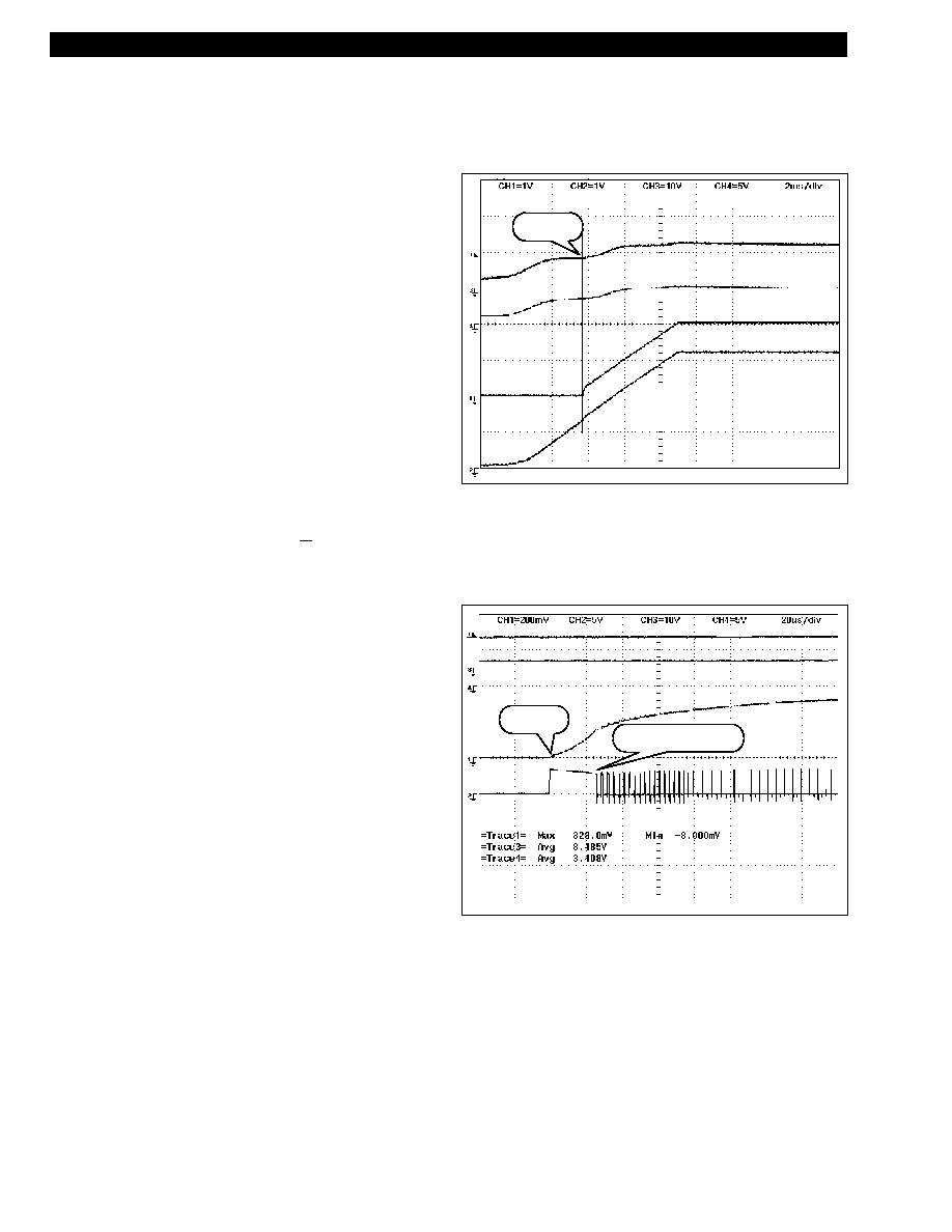
Figure 2: Normal Start-up (2ms/div).
Channel 1 - Regulator Output Voltage (1V/div)
Channel 2 - COMP Pin (1V/div)
Channel 3 - V
CC
(10V/div)
Channel 4 - Regulator Input Voltage (5V/div)
Figure 3: Normal Start-up showing initial pulse followed by Soft Start
(20µs/div).
Channel 1 - Regulator Output Voltage (0.2V/div)
Channel 2 – Inductor Switching Node (5V/div)
Channel 3 - V
CC
(10V/div)
Channel 4 - Regulator Input Voltage (5V/div)
Start-up @
V
CC
> 8.4V
Initial Pulse until V
OUT
> COMP - PWM Offset
Start-up @
V
CC
> 8.4V
T
L
Application Information: continued
8
CS5132

Figure 4: Pulse-by-Pulse Regulation during Soft Start (2µs/div).
Channel 1 - Regulator Output Voltage (0.2V/div)
Channel 2 – Inductor Switching Node (5V/div)
Channel 3 - V
CC
(10V/div)
Channel 4 - Regulator Input Voltage (5V/div)
Figure 5: Start-up with COMP pre-charged to 2V (2ms/div).
Channel 1 - Regulator Output Voltage (1V/div)
Channel 2 - COMP Pin (1V/div)
Channel 3 - V
CC
(10V/div)
Channel 4 - Regulator Input Voltage (5V/div)
When driving large capacitive loads, the COMP must
charge slowly enough to avoid tripping the CS5132 over-
current protection. The following equation can be used to
ensure unconditional start-up.
<
where
I
CHG
= COMP Source Current (30µA typical);
C
COMP
= COMP Capacitor value (0.1µF typical);
I
LIM
= Current Limit Threshold;
I
LOAD
= Load Current during start-up;
C
OUT
= Total Output Capacitance.
Normal Operation
During Normal operation, Switch Off-Time is constant and
set by the C
OFF
capacitor. Switch On-Time is adjusted by
the V
2
TM
Control loop to maintain regulation. This results in
changes in regulator switching frequency, duty cycle, and
output ripple in response to changes in load and line.
Output voltage ripple will be determined by inductor rip-
ple current and the ESR of the output capacitors
Transient Response
The CS5132 V
2
TM
Control Loop’s 200ns reaction time pro-
vides unprecedented transient response to changes in input
voltage or output current. Pulse-by-pulse adjustment of
duty cycle is provided to quickly ramp the inductor current
to the required level. Since the inductor current cannot be
changed instantaneously, regulation is maintained by the
output capacitor(s) during the time required to slew the
inductor current.
Overall load transient response is further improved through
a feature called “Adaptive Voltage Positioning”. This tech-
nique pre-positions the output voltage to reduce total out-
put voltage excursions during changes in load.
Holding tolerance to 1% allows the error amplifiers refer-
ence voltage to be targeted +25mV high without compro-
mising DC accuracy. A “Droop Resistor”, implemented
through a PC board trace, connects the Error Amps feed-
back pin (V
FB
) to the output capacitors and load and carries
the output current. With no load, there is no DC drop
across this resistor, producing an output voltage tracking
the Error amps, including the +25mV offset. When the full
load current is delivered, a 50mV drop is developed across
this resistor. This results in output voltage being offset -
25mV low.
The result of Adaptive Voltage Positioning is that addition-
al margin is provided for a load transient before reaching
the output voltage specification limits. When load current
suddenly increases from its minimum level, the output is
pre-positioned +25mV. Conversely, when load current sud-
denly decreases from its maximum level, the output is pre-
positioned -25mV. For best Transient Response, a combina-
tion of a number of high frequency and bulk output capaci-
tors are usually used.
Slope Compensation
The V
2
TM
control method uses a ramp signal, generated by
the ESR of the output capacitors, that is proportional to the
ripple current through the inductor. To maintain regula-
tion, the V
2
TM
control loop monitors this ramp signal,
through the PWM comparator, and terminates the switch
on-time.
The stringent load transient requirements of modern micro-
processors require the output capacitors to have very low
ESR. The resulting shallow slope presented to the PWM
comparator, due to the very low ESR, can lead to pulse
width jitter and variation caused by both random or syn-
chronous noise.
I
LIM
– I
LOAD
C
OUT
I
CHG
C
COMP
Soft Start @
COMP > 1.06V
OCP @
V
CC
> 8.5V
Duty Cycle = V
OUT
/ V
IN
0.27V / 3.54V = 7%
ª
5.2%
Application Information: continued
9
CS5132
Adding slope compensation to the control loop, avoids
erratic operation of the PWM circuit, particularly at lower
duty cycles and higher frequencies, where there is not
enough ramp signal, and provides a more stable switch-
point.
The scheme that prevents that switching noise prematurely
triggers the PWM circuit consists of adding a positive volt-
age slope to the output of the Error Amplifier (COMP pin)
during an off-time cycle.
The circuit that implements this function for the syn-
chronous regulator section (V
CC(CORE)
) is shown in Figure 6.
Figure 6: Small RC filter provides the proper voltage ramp at the begin-
ning of each on-time cycle.
The ramp waveform is generated through a small RC filter
that provides the proper voltage ramp at the beginning of
each on-time cycle. The resistors R
1
and R
2
in the circuit of
Figure 6 form a voltage divider from the GATE(L) output,
superimposing a small artificial ramp on the output of the
error amplifier.
A similar approach can be used also for the non-syn-
chronous regulator section (V
I/O
) as shown in Figure 7. In
this case, the slope compensation signal is generated direct-
ly from the GATE output, through the ac coupling capaci-
tor C
1
, at the beginning of each on-cycle.
It is important that in both circuits, the series combination
R
1
/R
2
is high enough in resistance not to load down and
negatively affect the slew rate on the GATE(L) and GATE
pins.
Figure 7: Slope compensation for the non-synchronous regulator section
(V
I/O
).
Over-Current Protection
A loss-less hiccup mode current limit protection feature is
provided, requiring only the COMP capacitor to imple-
ment. The CS5132 provides overcurrent protection by sens-
ing the current through a “Droop” resistor, using an inter-
nal current sense comparator. The comparator compares
the voltage drop across the “Droop” resistor to an internal
reference voltage of 86mV (typical).
If the voltage drop across the “Droop” resistor exceeds this
threshold, the current sense comparator allows the fault
latch to be set. This causes the regulator to stop switching.
During this over current condition, the CS5132 stays off for
the time it takes the COMP pin capacitor to discharge to its
lower 0.25V threshold. As soon as the COMP pin reaches
0.25V, the Fault latch is reset (no overcurrent condition pre-
sent) and the COMP pin is charged with a 30µA current
source to a voltage 1.06V greater than the V
FFB
voltage.
Only at this point the regulator attempts to restart normal-
ly. The CS5132 will operate initially with a duty cycle
whose value depends on how low the V
FFB
voltage was
during the overcurrent condition (whether hiccup mode
was due to excessive current or hard short). This protection
scheme minimizes thermal stress to the regulator compo-
nents, input power supply, and PC board traces, as the over
current condition persists. Upon removal of the overload,
the fault latch is cleared, allowing normal operation to
resume.
Overvoltage Protection
Overvoltage protection (OVP) is provided as result of the
normal operation of the V
2
TM
control topology and requires
no additional external components. The control loop
responds to an overvoltage condition within 200ns, causing
the top MOSFET to shut off, disconnecting the regulator
from its input voltage. This results in a “crowbar” action to
clamp the output voltage and prevents damage to the load.
The regulator will remain in this state until the overvoltage
condition ceases or the input voltage is pulled low.
Additionally, a dedicated Overvoltage protection (OVP)
output pin (pin 21) is provided in the CS5132. The OVP sig-
nal will go high (overvoltage condition), if the output volt-
age (V
CC(CORE)
) exceeds the regulation voltage by 8.5% of
the voltage set by the particular DAC code. The OVP pin
can source up to 25mA of current that can be used to drive
an SCR to crowbar the power supply.
Power-Good Circuit
The Power-Good pin (pin 22) is an open-collector signal
consistent with TTL DC specifications. It is externally
pulled up, and is pulled low (below 0.3V) when the regula-
tor output voltage typically exceeds ± 8.5% of the nominal
output voltage. Maximum output voltage deviation before
Power-Good is pulled low is ± 12%.
Output Enable
On/off control of the regulator outputs can be implement-
ed by pulling the COMP pins low. It is required to pull the
COMP pins below the 1.06V PWM comparator offset volt-
age in order to disable switching on the GATE drivers.
Protection and Monitoring Features
R
1
C
1
15
13
GATE
COMP2
CS5132
To V
I/O
Power Switch
C
COMP2
R
2
C
COMP
R
1
To Synchronous FET
C
1
R
2
5
19
COMP1
GATE(L)
CS5132
Application Information: continued
10
CS5132

Step 1: Define Specification
Input Voltage from “silver box” power supply
• 5V ±5% for conversion to output voltage
• 12V ±5% for NFET Gate Voltage and circuit bias
Output Voltages
• 2.0V @ 16A for V
CC(CORE)
• 3.3V@ 8A for V
I/O
• 5% Overall Voltage accuracy (load, line, temperature,
ripple)
• 2% DC & 5% AC Voltage Accuracy
• < 2% Output Ripple Voltage
• 15A Load Step @ 20A /µs - V
CC(CORE)
• 7A Load Step @ 5A/µs - V
I/O
Thermal Management
• 0 to 50˚ C ambient temperature range
• Component junction temperatures within manufactur-
er’s specified ratings at full load & T
A(MAX)
Components
• Low cost is top priority.
• Surface mount when possible
• Small footprint important
• Component Ratings determined at 80% of Maximum
Load
Step 2: Determine Output Capacitors
These components must be selected and placed carefully to
yield optimal results. Capacitors should be chosen to pro-
vide acceptable ripple on the regulator output voltage. Key
specifications for input capacitors are their ripple rating,
while ESR is important for output capacitors. For best tran-
sient response, a combination of low value/high frequency
and bulk capacitors placed close to the load will be
required.
Step 2a: For the 2V Output (V
CC(CORE)
)
The load transients have slew rates of up to 20A /µs, while
the voltage drop during a transient must be kept to less
than 100mV. The output capacitors must hold the output
voltage within these limits since the inductor current can
not change with the required slew rate. The output capaci-
tors must therefore have a very low ESL and ESR.
The voltage transient during the load step is
DV
OUT
=
DI
OUT
¥
(
+ ESR +
)
,
where t
TR
= output voltage transient response time.
The total change in output voltage is divided as follows:
ESR - 80mV
ESL - 10mV
Output Capacitor Discharge During Transient - 10mV
Maximum allowable ESR is:
ESR =
= 5.3mΩ.
The ESR for a 1200µF/10V Sanyo capacitor type GX is
44mΩ per capacitor.
Number of Capacitors =
@ 8.
Total ESR =
= 5.5mΩ.
Output voltage deviation due to ESR:
DV = 15A ¥ 5.5mΩ = 82mV.
The ESL is calculated from
= ,
ESL =
=
= 0.5nH.
It is estimated that a 10
¥ 12 mm Aluminum Electrolytic
capacitor has approximately 4nH of package inductance. In
this case we have eight (8) capacitors in parallel for a total
capacitor ESL:
ESL =
= 0.5nH.
Output voltage deviation due to ESL:
DV =
=
= 10mV.
The change in capacitor voltage during the transient is:
DV
C
=
,
where t
TR
is the output voltage transient response time. We
choose t
TR
= 6µs:
DV
C
=
= 9mV.
Total change in output voltage as a result of an increase in
load current of a 15A step with a 20A/µs slew rate is:
DV
OUT
= ( 82mV + 10mV + 9mV ) = 101mV.
Step 2b: For the 3.3V Output (V
I/O
)
The V
I/O
load transients have slew rates of 5A/µs, while
the voltage drop during a transient must be kept to less
15A
¥ 6µs
8
¥ 1200µF
DI ¥ t
TR
C
OUT
0.5nH
¥ 20A
1µs
ESL
¥ DI
Dt
4nH
8
0.01V
¥ 1 ¥ 10
-6
20
DV ¥ Dt
DI
20A
µs
DI
Dt
44
8
44
5.3
0.08V
15A
t
TR
C
OUT
ESL
Dt
CS5132-based Dual Output
Buck Regulator Design Example
Application Information: continued
11
CS5132

than ±165mV. Repeating step 2a, we select four (4)
1200µF/10V Sanyo GX output capacitors.
Step 3: Duty Cycle, Switching Frequency, T
ON
& T
OFF
Duty Cycle
ª V
OUT
/ V
IN.
D = 2.0V / 5V = 40% for 2V output.
D = 3.3V / 5V = 66% for 3.3V output.
Select 200kHz Switching Frequency (F
SW
).
Step 3a: Calculate On-Time for 2V Output
T
ON
=
=
= 2µs
Calculate Off-Time:
T
OFF =
= 5µs - 2µs = 3µs.
Select the C
OFF1
capacitor in order to set the Off-Time:
C
OFF1
= =
=
750pF.
A standard C
OFF1
capacitance value of 680pF can be used.
The 3980 factor is a characteristic of the CS5132.
Step 3b: Calculate On-Time for 3.3V Output
T
ON
=
=
= 3.3µs
Calculate Off-Time:
T
OFF
=
- T
ON
= 5µs – 3.3µs = 1.7µs.
Select C
OFF2
to be 390pF.
Step 4: Output Inductor
The inductor should be selected based on its inductance,
current capability, and DC resistance. Increasing the induc-
tor value will decrease output voltage ripple, but degrade
transient response. There are many factors to consider in
selecting the inductor including: cost, efficiency, EMI and
ease of manufacture. The inductor must be able to handle
the peak current at the switching frequency without satu-
rating, and the copper resistance in the winding should be
kept as low as possible to minimize resistive power loss.
There are a variety of materials and types of magnetic
cores that could be used for this application. Among them
are: ferrites, molypermalloy cores (MPP), amorphous and
powdered iron cores. We will use a powdered iron core.
Iron powdered cores are very suitable due to their high sat-
uration flux density and have low loss at high frequencies,
a distributed gap and exhibit very low EMI.
Calculate Inductor Value:
L=
= =
=1.2µH.
Step 4a: Select 2% Ripple on 2V Output
DV
OUT
= 2%
¥ 2V = 40mV
The maximum allowable Inductor Ripple Current for a 2%
ripple on the 2V output is:
DI
L
=
= =
7.3A,
which corresponds to the following maximum Inductor
Peak and Valley currents:
I
L(PEAK)
= I
OUT
+
( )
= 16A +
(
)
= 19.6A,
I
L(VALLEY)
= I
OUT
-
( )
= 16A -
(
)
= 12.4A.
The selected 1.2µH inductor yields the following ripple
current:
DI
L
=
=
= 5A.
The maximum inductor peak current becomes:
I
L(PEAK)
= 16A +
= 16A + 2.5A = 18.5A.
The inductor valley current becomes:
I
L(VALLEY)
= 16A -
= 16A - 2.5A = 13.5A.
The above values are well within the maximum allowable
inductor peak and valley currents for a 2% output voltage
ripple.
Select Toroid Powdered Iron Core, low cost, low core loss-
es at 200kHz, low EMI.
Select XFMRS Inc, XF0016-VO4 1.2µH inductor with R
DC
=
0.003Ω typical, 0.008Ω maximum.
Step 4b: Select 2% Ripple on 3.3V Output
Repeating Step 4a for the 3.3V output, we find 3.5µH is a
suitable value for this output.
Step 5: Input Capacitors
These components must be selected and placed carefully to
yield optimal results. Capacitors should be chosen to pro-
vide acceptable ripple on the input supply lines. Key speci-
fications for input capacitors are their ripple rating.
Step 5a: V
CC(CORE)
Buck Regulator Input Capacitors
The input capacitor C
IN
should also be able to handle the
5A
2
5A
2
(5V - 2V)
¥ 0.4
200kHz
¥ 1.2µH
(V
IN
- V
OUT
)
¥ D
F
SW
¥ L
7.3A
2
DI
L
2
7.3A
2
DI
L
2
40mV
5.5mΩ
DV
OUT
Total ESR
3V
¥ 6µs
15A
(5V-2V)
¥ 6µs
15A
(V
IN
- V
OUT
) t
TR
DI
1
F
SW
0.66
200kHz
D
F
SW
5µs
¥ 0.6
3980
Period
¥ (1-D)
3980
- T
ON
1
F
SW
0.40
200kHz
D
F
SW
Application Information: continued
12
CS5132

input RMS current I
IN(RMS)
. C
IN
discharges during the on-
time.
The discharge current is given by:
I
CINDISRMS
=
= 10.2A.
C
IN
charges during the off-time, the average current
through the capacitor over one switching cycle is zero:
I
CIN(CH)
= I
CIN(DIS)
¥
,
I
CIN(CH)
= 10.2A
¥
= 6.8A.
So the total Input RMS current is:
I
CIN(RMS)
= (I
CIN(DIS)
2
¥ D) +(
I
CIN(CH)
2
¥ (1-D)
),
I
CIN(RMS)
=
.
The number of input capacitors required is given by:
N
CIN
=
.
For Sanyo capacitors type GX:
1200µF/10V
,
I
RIPPLE
= 1.25A.
Hence,
N
CIN
= =
6.6.
The number of input capacitors can be rounded off to 6.
Calculate the Input Capacitor Ripple Voltage:
V
RMS
= I
RMS
¥ Total ESR = 8.3A ¥ 7.3mΩ = 60mV.
Calculate the Input Capacitor Power Loss:
P
CIN
= I
RMS
2
¥ Total ESR = 0.504W.
Step 5b: V
I/O
Buck Regulator Input Capacitors
Repeating for the 3.3V output, we select 3 GX 1200µF/10V
capacitors.
Step 6: Power MOSFETs
FET Basics
The use of the MOSFET as a power switch is propelled by
two reasons: 1) Its very high input impedance and 2) Its
very fast switching times. The electrical characteristics of a
MOSFET are considered to be those of a perfect switch.
Control and drive circuitry power is therefore reduced.
Because the input impedance is so high, it is voltage driv-
en. The input of the MOSFET acts as if it were a small
capacitor, which the driving circuit must charge at turn on.
The lower the drive impedance, the higher the rate of rise
of V
GS
, and the faster the turn- on time. Power dissipation
in the switching MOSFET consists of 1) conduction losses,
2) leakage losses, 3) turn-on switching losses, 4) turn-off
switching losses, and 5) gate-transitions losses. The latter
three losses are proportional to frequency. For the conduct-
ing power dissipation rms values of current and resistance
are used for true power calculations.
The fast switching speed of the MOSFET makes it indis-
pensable for high-frequency power supply applications.
Not only are switching power losses minimized, but the
maximum usable switching frequency is considerably
higher. Switching time is independent of temperature.
Also, at higher frequencies, the use of smaller and lighter
components (transformer, filter choke, filter capacitor)
reduces overall component cost while using less space for
more efficient packaging at lower weight.
The MOSFET has purely capacitive input impedance. No
DC current is required. It is important to keep in mind the
drain current of the FET has a negative temperature coeffi-
cient. Increase in temperature causes higher on-resistance
and greater leakage current.
For switching circuits, V
DS(ON)
should be low to minimize
power dissipation at a given I
D
, and V
GS
should be high to
accomplish this. MOSFET switching times are determined
by device capacitances, stray capacitances, and the
impedance of the gate drive circuit. Thus the gate driving
circuit must have high momentary peak current sourcing
and sinking capability for switching the MOSFET. The
input capacitance, output capacitance and reverse-transfer
capacitance also increase with increased device current
rating.
Two considerations complicate the task of estimating
switching times. First, since the magnitude of the input
capacitance, C
ISS
, varies with V
DS
, the RC time constant
determined by the gate-drive impedance and C
ISS
changes
during the switching cycle. Consequently, computation of
the rise time of the gate voltage by using a specific gate-
drive impedance and input capacitance yields only a rough
estimate. The second consideration is the effect of the
"Miller" capacitance, C
RSS
, which is referred to as C
dg
in the
following discussion. For example, when a device is on,
V
DS
is fairly small and V
GS
is about 12V. C
dg
is charged to
V
DS(ON)
- V
GS
, which is a negative potential if the drain is
considered the positive electrode. When the drain is "off",
C
dg
is charged to quite a different potential. In this case the
voltage across C
dg
is a positive value since the potential
from gate-to-source is near zero volts and V
DS
is essentially
the drain supply voltage. During turn-on and turn-off,
8.3
1.25
I
CIN(RMS)
I
RIPPLE
(10.2
2
¥ 0.4) + (6.8
2
(
¥ 0.6)) = 8.3A
0.4
(1-0.4)
D
1-D
(I
L(PEAK)
2
+ (I
L(PEAK)
¥ I
L(VALLEY)
)
+ I
L(VALLEY
2
)
¥ D
3
Application Information: continued
13
CS5132

these large swings in gate-to-drain voltage tax the current
sourcing and sinking capabilities of the gate drive. In addi-
tion to charging and discharging C
GS
, the gate drive must
also supply the displacement current required by C
dg
(I
GATE
= C
dg
dV
dg
/dt). Unless the gate-drive impedance is
very low, the V
GS
waveform commonly plateaus during
rapid changes in the drain-to-source voltage.
The most important aspect of FET performance is the Static
Drain-To-Source On-Resistance (RDS
ON
), which effects
regulator efficiency and FET thermal management require-
ments. The On- Resistance determines the amount of cur-
rent a FET can handle without excessive power dissipation
that may cause overheating and potentially catastrophic
failure. As the drain current rises, especially above the con-
tinuous rating, the On-Resistance also increases. Its posi-
tive temperature coefficient is between +0.6%/C and
+0.85 %/C. The higher the On-Resistance the larger the
conduction loss is.
Both logic level and standard FETs can be used. The refer-
ence designs derive gate drive from the 12V supply which
is generally available in most computer systems and uti-
lizes logic level FETs. Multiple FETs may be paralleled to
reduce losses and improve efficiency and thermal manage-
ment.
Voltage applied to the FET gates depends on the applica-
tion circuit used. Both upper and lower gate driver outputs
are specified to drive to within 1.5V of ground when in the
low state and to within 2V of their respective bias supplies
when in the high state. In practice, the FET gates will be
driven rail-to-rail due to overshoot caused by the capaci-
tive load they present to the controller IC.
We select Mitsubishi’s FS70VSJ-03 (D
2
package):
30V withstand voltage; RDS
ON
= 8m
W; QJA = 40˚C/W;
Total Gate Charge = 50nC.
Step 6a: For the 2V Output Upper (Switching) FET
Calculate the 2V Output’s Maximum RMS Current through
the Switch:
I
RMS(H)
=
= 10.2A.
Calculate Switch Conduction Losses:
P
RMS
= I
RMS
2
¥ RDS
ON
= 10.2A
2
¥ 8mΩ = 0.83W.
Calculate Switching Losses:
Switch On Losses:
P
SW(ON)
=
,
T
RISE
= 60ns,
(from Mitsubishi FS70VSJ-03 switching characteristics per-
formance curves):
T =
= 5µs,
P
SW(ON)
=
= 0.16W.
Switch Off Losses:
P
SW(OFF)
=
,
T
FALL
= 160ns,
(from Mitsubishi FS70VSJ-03 switching characteristics per-
formance curves):
P
SW(OFF)
=
= 0.43W.
Upper FET Total Losses = Switching Conduction Losses +
Switch On Losses + Switch Off Losses:
P
FETH(TOTAL)
= 0.83W + 0.16W + 0.43W = 1.42W.
Calculate Maximum NFET Switch Junction Temperature:
T
J
= T
A
+ [(P
FETH(TOTAL)
)
¥ Q
JA
],
T
J
= 50C + (1.412W)
¥ 40˚C/W = 107°C.
Calculate the Gate Driver Losses:
P
GATE(H)
= Q
¥ V
GATE
¥ F
SW
= 50nC
¥ 12V ¥ 200KHz = 120mW.
Step 6b: Similar calculations apply for the 3.3V output.
Step 6c: Synchronous FET ( 2V Output)
Calculate Switch Conduction Losses:
P
RMS
= I
RMS
2
¥ RDS
ON
= [I
OUT
2
¥ (1-D)] ¥ RDS
ON
= [16A
2
¥ 0.6] ¥ 8mW = 1.22W.
The synchronous MOSFET has no switching losses, except
for losses in the internal body diode, because it turns on
into near zero voltage conditions. The MOSFET body diode
will conduct during the non-overlap time and the resulting
power dissipation (neglecting reverse recovery losses) can
be calculated as follows:
P
SW
= V
SD
¥ I
LOAD
¥ non-overlap time
¥ switching frequency.
From the Mitsubishi FS70VSJ-03 source-drain diode for-
ward characteristics curve, V
SD
= 0.8V:
P
SW
= 0.8V
¥ 16A ¥ 65ns ¥ 200kHz,
P
SW
= 0.16W.
5V
¥ 16A ¥ 160 ¥ 10
-9
6
¥ 5 ¥ 10
-6
V
IN
¥ I
OUT
¥ T
FALL
6T
5V
¥ 16A ¥ 60¥ 10
-9
6
¥ 5 ¥ 10
-6
1
F
SW
(V
IN
¥ I
OUT
¥ T
RISE
)
6T
(I
L(PEAK)
2
+ (I
L(PEAK)
¥ I
L(VALLEY)
)
+ I
L(VALLEY
2
)
¥ D
3
Application Information: continued
14
CS5132

Lower (Synchronous) FET Total Losses = Switch Conduc-
tion Losses + Body Diode Losses:
P
FETL(TOTAL)
= 1.27W + 0.16W =1.43W.
Calculate Maximum NFET Switch Junction Temperature:
T
J
= T
A
+ [(P
FETL(TOTAL)
)
¥ Q
JA
],
T
J
= 50C + (1.43W)
¥ 40˚C/W = 107°C.
Calculate the Gate Driver Losses:
P
GATE(L)
= Q
¥ V
GATE
¥ F
SW
= 50nC
¥ 12V ¥ 200KHz = 120mW.
Step 7: Free Wheeling Schottky Diode (3.3V Output)
The four most application-important characteristics of a
Schottky are:
1. Forward voltage drop;
2. Reverse leakage current;
3. Reverse blocking voltage;
4. Maximum permissible junction temperature.
We calculate the average Schottky current:
I
AVG
= I
OUT
¥ (1-D) = 8A ¥ 0.34 = 2.72A.
We select the Motorola MBRD835L rated at 8A, with 35V
DC blocking voltage and 0.51Vforward voltage drop.
Neglecting reverse losses, the power dissipation is due to
the conduction loss only and can be computed as follows:
P
SCHOTTKY
= V
F
¥ I
AVG
,
where
V
F
= maximum instantaneous forward voltage;
P
SCHOTTKY
= 0.51V
¥ 2.72A = 1.39W.
Calculate maximum Schottky junction temperature:
T
J
= T
A
+ [(P
SCHOTTKY
)
¥ Q
JA
],
T
J
= 50C + (1.39W
¥ 80˚C/W) = 161°C.
Proper heatsinking (copper pad under Schottky) will be
required to reduce Schottky T
J
below +125˚C.
Step 8: IC Power Dissipation
The power dissipation on the IC varies with the MOSFETs
used, V
CC
and the CS5132 operating frequency. This power
dissipation is typically dominated by the average gate
charge current for the MOSFETs. The average current is
approximately:
I
D
= (Q
GATE(H)
+ Q
GATE(L)
)
¥ F
SW1
+ Q
GATE
¥ F
SW2
,
where
I
D
= average drive current;
Q
GATE(X)
= total gate charge for each MOSFET;
F
SW1
, F
SW2
= switching frequencies for the synchronous
and non-synchronous sections respectively.
The power dissipation for the IC when V
CC1
= V
CC2
=
V
CC
is:
P
D
= I
CC
¥ V
CC
+ I
D
¥ V
CC
,
where
I
CC
= quiescent supply current of the IC (both from V
CC1
and V
CC2
).
For the design example in question,
P
D
= 19mA
¥ 12V + 0.12W + 0.12W + 0.12W = 0.59W.
The junction temperature of the IC is primarily a function
of the PCB layout, since most of the heat is removed
through the traces connected to the pins of the IC.
Adaptive voltage positioning is used to help keep the out-
put voltage within specification during load transients. To
implement adaptive voltage positioning a “Droop
Resistor” must be connected between the output inductor
and output capacitors and load. This resistor carries the
full load current and should be chosen so that both DC and
AC tolerance limits are met. An embedded PC trace resis-
tor has the distinct advantage of near zero cost implemen-
tation. However, this droop resistor can vary due to three
reasons: 1) the sheet resistivity variation caused by varia-
tion in the thickness of the PCB layer; 2) the mismatch of
L/W; and 3) temperature variation.
1) Sheet Resistivity
For one ounce copper, the thickness variation is typically
1.26 mil to 1.48 mil. Therefore the error due to sheet resis-
tivity is:
= ±8%.
2) Mismatch due to L/W
The variation in L/W is governed by variations due to the
PCB manufacturing process. The error due to L/W mis-
match is typically 1%.
3) Thermal Considerations
Due to I
2
¥ R power losses the surface temperature of the
droop resistor will increase causing the resistance to
increase. Also, the ambient temperature variation will con-
tribute to the increase of the resistance, according to the
formula:
R = R
20
[1+
a
20
(T-20)],
1.48 - 1.26
1.37
“Droop” Resistor for Adaptive Voltage Positioning
and Current Limit
Application Information: continued
15
CS5132

where
R
20
= resistance at 20˚C;
a =
;
T
= operating temperature;
R = desired droop resistor value.
For temperature T = 50˚C, the % R change = 12%.
Droop Resistor Tolerance
Tolerance due to sheet resistivity variation
±8%
Tolerance due to L/W error
1%
Tolerance due to temperature variation
12%
Total tolerance for droop resistor
21%
In order to determine the droop resistor value the nominal
voltage drop across it at full load has to be calculated. This
voltage drop has to be such that the output voltage at full
load is above the minimum DC tolerance spec:
V
DROOP(TYP)
= .
Example: for a 450MHz Pentium
®
II, the DC accuracy spec
is 1.93 < V
CC(CORE)
< 2.07V, and the AC accuracy spec is
1.9V < V
CC(CORE)
< 2.1V. The CS5132 DAC output voltage is
+2.004V < V
DAC
< +2.045V. In order not to exceed the DC
accuracy spec, the voltage drop developed across the resis-
tor must be calculated as follows:
V
DROOP(TYP)
=
=
= 61mV.
With the CS5132 DAC accuracy being 1%, the internal error
amplifier’s reference voltage is trimmed so that the output
voltage will be 25mV high at no load. With no load, there is
no DC drop across the resistor, producing an output volt-
age tracking the error amplifier output voltage, including
the offset. When the full load current is delivered, a drop of
-50mV is developed across the resistor. Therefore, the regu-
lator output is pre-positioned at 25mV above the nominal
output voltage before a load turn-on. The total voltage
drop due to a load step is ∆V-25mV and the deviation from
the nominal output voltage is 25mV smaller than it would
be if there was no droop resistor. Similarly at full load the
regulator output is pre-positioned at 25mV below the nom-
inal voltage before a load turn-off. the total voltage increase
due to a load turn-off is ∆V-25mV and the deviation from
the nominal output voltage is 25mV smaller than it would
be if there was no droop resistor. This is because the output
capacitors are pre-charged to a value that is either 25mV
above the nominal output voltage before a load turn-on or,
25mV below the nominal output voltage before a load turn-
off .
Obviously, the larger the voltage drop across the droop
resistor (the larger the resistance), the worse the DC and
load regulation, but the better the AC transient response.
Current Limit
The current limit setpoint has to be higher than the normal
full load current. Attention has to be paid to the current
rating of the external power components as these are the
first to fail during an overload condition. The MOSFET
continuous and pulsed drain current rating at a given case
temperature has to be accounted for when setting the cur-
rent limit trip point.
Temperature curves on MOSFET manufacturers’ data
sheets allow the designer to determine the MOSFET drain
current at a particular V
GS
and T
J
(junction temperature).
This, in turn, will assist the designer to set a proper current
limit, without causing device breakdown during an over-
load condition.
For future “CPUs” the full load will be 16A. The internal
current sense comparator current limit voltage limits are:
77mV < V
TH
< 101mV. Also, there is a 21% total variation
in R
SENSE
as discussed in the previous section.
We compute the value of the current sensing element
(embedded PCB trace) for the minimum current limit set-
point:
R
SENSE(MIN)
= R
SENSE(TYP)
¥ 0.79,
R
SENSE(MAX)
= R
SENSE(TYP)
¥ 1.21,
R
SENSE(MAX)
= =
=
4.8mΩ.
We select,
R
SENSE(TYP)
= 3.3mΩ.
We calculate the range of load currents that will cause the
internal current sense comparator to detect an overload
condition.
Nominal Current Limit Setpoint
From the overcurrent detection data in the electrical char-
acteristics table:
V
TH(TYP)
= 86mV,
I
CL(NOM)
=
=
= 26A.
Maximum Current Limit Setpoint
From the overcurrent detection data in the electrical char-
acteristics table:
V
TH(MAX)
= 101mV,
I
CL(MAX)
=
=
= =
38.7A.
101mV
3.3mΩ
¥ 0.79
V
TH(MAX)
R
SENSE(NOM)
¥ 0.79
V
TH(MAX)
R
SENSE(MIN)
86mV
3.3mΩ
V
TH(TYP)
R
SENSE(NOM)
77mV
16A
V
TH(MIN)
I
CL(MIN)
+2.004V-1.93V
1.21
[V
DAC(MIN)
-V
DC (MIN)
]
1+R
DROOP(TOLERANCE)
V
DAC(MIN)
-V
DC(MIN)
1+R
DROOP(TOLERANCE)
0.00393
˚C
16
Application Information: continued
CS5132

Application Information: continued
Therefore, the range of load currents that will cause the
internal current sense comparator to detect an overload
condition through a 3.3mΩ embedded PCB trace is: 19.3A
< I
CL
< 38.7A, with 26A being the nominal overload condi-
tion.
Design Rules for Using a Droop Resistor
The basic equation for laying an embedded resistor is:
R
AR
=
r ¥
or R =
r ¥
,
where
A= W
¥ t = cross-sectional area;
r= the copper resistivity (µΩ-mil);
L= length (mils);
W = width (mils);
t = thickness (mils).
For most PCBs the copper thickness, t, is 35µm (1.37 mils)
for one ounce copper;
r = 717.86µΩ-mil.
For a CPU load of 16A the resistance needed to create a
50mV drop at full load is:
R
DROOP
=
=
= 3.1mΩ.
The resistivity of the copper will drift with the temperature
according to the following guidelines:
∆R = 12% @ T
A
= +50˚C;
∆R = 34% @T
A
= +100˚C.
Droop Resistor Length, Width, and Thickness
The minimum width and thickness of the droop resistor
should primarily be determined on the basis of the current-
carrying capacity required, and the maximum permissible
droop resistor temperature rise. PCB manufacturer design
charts can be used in determining current- carrying capaci-
ty and sizes of etched copper conductors for various tem-
perature rises above ambient.
For single conductor applications, such as the use of the
droop resistor, PCB design charts show that for a droop
resistor with a required current-carrying capacity of 16A,
and a 45˚C temperature rise above ambient, the recom-
mended cross section is 275 mil
2
.
W
¥ t = 275 mil
2
,
where
W = droop resistor width;
t = droop resistor thickness.
For 1oz. copper, t= 1.37 mils, therefore W = 201 mils =
0.201 in.
R =
r ¥
,
where
R = droop resistor value;
r = 0.71786mW-mil (1 oz. copper);
L = droop resistor length;
W = droop resistor width.
R
DROOP
= 3.3m
W.
3.3m
W = 0.71786mW-mil ¥
.
Hence, L = 1265 mils = 1.265 in.
In layouts where it is impractical to lay out a droop resistor
in a straight line 1265 mils long, the embedded PCB trace
can be “snaked” to fit within the available space.
Thermal Considerations for Power MOSFETs and Diodes
In order to maintain good reliability, the junction tempera-
ture of the semiconductor components should be kept to a
maximum of 150°C or lower. The thermal impedance
(junction to ambient) required to meet this requirement can
be calculated as follows:
Thermal Impedance =
.
A heatsink may be added to TO-220 components to reduce
their thermal impedance. A number of PC board layout
techniques such as thermal vias and additional copper foil
area can be used to improve the power handling capability
of surface mount components.
As a consequence of large currents being turned on and off
at high frequency, switching regulators generate noise as a
consequence of their normal operation. When designing
for compliance with EMI/EMC regulations, additional
components may be added to reduce noise emissions.
These components are not required for regulator operation
and experimental results may allow them to be eliminated.
The input filter inductor may not be required because bulk
filter and bypass capacitors, as well as other loads located
on the board will tend to reduce regulator di/dt effects on
the circuit board and input power supply. Placement of the
power component to minimize routing distance will also
help to reduce emissions.
EMI Management
T
J(MAX)
- T
A
Power
Thermal Management
L
201 mils
¥ 1.37 mils
L
W
¥ t
50mV
16A
50mV
I
OUT
L
(W
¥ t)
L
A
17
CS5132

18
Application Information: continued
CS5132
When laying out the CPU buck regulator on a printed cir-
cuit board, the following checklist should be used to ensure
proper operation of the CS5132.
1) Rapid changes in voltage across parasitic capacitors and
abrupt changes in current in parasitic inductors are major
concerns for a good layout.
2) Keep high currents out of sensitive ground connections.
Avoid connecting the IC Gnd between the source of the
lower FET and the input capacitor Gnd.
3) Avoid ground loops as they pick up noise. Use star or
single point grounding.
4) For high power buck regulators on double-sided PCBs a
single ground plane (usually the bottom) is recommended.
5) Even though double sided PCBs are usually sufficient
for a good layout, four-layer PCBs are the optimum
approach to reducing susceptibility to noise. Use the two
internal layers as the power and Gnd planes, the top layer
for the high current connections and component vias, and
the bottom layer for the noise sensitive traces.
6) Keep the inductor switching node small by placing the
output inductor, switching and synchronous FETs close
together.
7) The MOSFET gate traces to the IC must be as short,
straight, and wide as possible. Ideally, the IC has to be
placed right next to the MOSFETs.
8) Use fewer, but larger output capacitors, keep the capaci-
tors clustered, and use multiple layer traces with heavy
copper to keep the parasitic resistance low.
9) Place the switching MOSFET as close to the +5V input
capacitors as possible.
10) Place the output capacitors as close to the load
as possible.
11) Place the V
FFB
,V
OUT
filter resistors (510Ω) in series with
the V
FFB
and V
OUT
pins as close as possible to the pins.
12) Place the C
OFF
and COMP capacitors as close as possi-
ble to the C
OFF
and COMP pins.
13) Place the current limit filter capacitors between the
V
FFB
and V
OUT
pins, as close as possible to the pins.
14) Connect the filter components of the following pins:
V
FB
, V
FFB
, V
OUT
, C
OFF
, and COMP to the LGnd pin with a
single trace, and connect this local LGnd trace to the output
capacitor Gnd.
15) The “Droop” Resistor (embedded PCB trace) has to be
wide enough to carry the full load current.
16) Place the V
CC
bypass capacitors as close as possible to
the V
CC
pins and connect them to PGnd.
Layout Guidelines
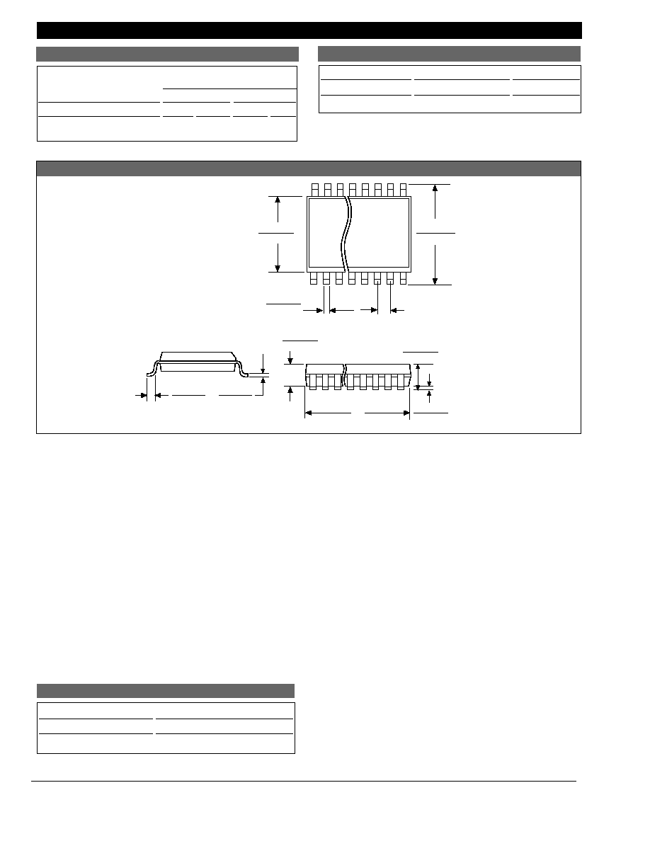
CS5132
19
Part Number
Description
CS5132GDW24
24L SO Wide
CS5132GDWR24
24L SO Wide (tape & reel)
Rev. 11/3/98
D
Lead Count
Metric
English
Max
Min
Max
Min
24L SO Wide
15.60
15.20
.614
.598
Thermal Data
24L SO Wide
R
QJC
typ
16
˚C/W
R
QJA
typ
80
˚C/W
Package Specification
PACKAGE DIMENSIONS IN mm (INCHES)
PACKAGE THERMAL DATA
Ordering Information
© 1999 Cherry Semiconductor Corporation
Cherry Semiconductor Corporation reserves the right to
make changes to the specifications without notice. Please
contact Cherry Semiconductor Corporation for the latest
available information.
Surface Mount Wide Body (DW); 300 mil wide
1.27 (.050) BSC
7.60 (.299)
7.40 (.291)
10.65 (.419)
10.00 (.394)
D
0.32 (.013)
0.23 (.009)
1.27 (.050)
0.40 (.016)
REF: JEDEC MS-013
2.49 (.098)
2.24 (.088)
0.51 (.020)
0.33 (.013)
2.65 (.104)
2.35 (.093)
0.30 (.012)
0.10 (.004)