
The CS5150 is a 4-bit synchronous
dual N-Channel buck controller. It
is designed to provide unprece-
dented transient response for
today's demanding high-density,
high-speed logic. The regulator
operates using a proprietary control
method, which allows a 100ns
response time to load transients.
The CS5150 is designed to operate
over a 4.25-16V range (V
CC
) using
12V to power the IC and 5V as the
main supply for conversion.
The CS5150 is specifically designed
to power Pentium
Æ
Pro processors
and other high performance core
logic. It includes the following fea-
tures: on board, 4-bit DAC, short
circuit protection, 1.0% output tol-
erance, V
CC
monitor, and pro-
grammable soft start capability. The
CS5150 is upward compatible with
the 5-bit CS5155, allowing the
mother board designer the capabili-
ty of using either the CS5150 or the
CS5155 with no change in layout.
The CS5150 is available in 16 pin
surface mount and DIP packages.
Features
s
Dual N-Channel Design
s
Excess of 1MHz Operation
s
100ns Transient Response
s
4-Bit DAC
s
Upward Compatible with
5-Bit CS5155/5156 and
Adjustable CS5120/5121
s
30ns Gate Rise/Fall Times
s
1% DAC Accuracy
s
5V & 12V Operation
s
Remote Sense
s
Programmable Soft Start
s
Lossless Short Circuit
Protection
s
V
CC
Monitor
s
25ns FET Nonoverlap Time
s
Adaptive Voltage
Positioning
s
V
2
TM Control Topology
s
Current Sharing
s
Overvoltage Protection
Package Options
CPU 4-Bit Synchronous Buck Controller
CS5150
Description
Application Diagram
1
V
ID0
V
ID1
V
ID2
V
ID3
SS
NC
C
OFF
V
FFB
V
FB
COMP
LGnd
V
CC1
V
GATE(L)
PGnd
V
GATE(H)
V
CC2
16 Lead SO Narrow & PDIP
1
Switching Power Supply for core logic - Pentium
Æ
Pro processor
0.33
µ
F
V
ID0
V
ID1
V
ID2
V
ID3
V
ID0
V
ID1
V
ID2
V
ID3
V
CC1
SS
CS5150
C
OFF
LGnd
V
FB
V
FFB
COMP
IRL3103
IRL3103
0.1
µ
F
12V
5V
2
µ
H
2.1V to 3.5V @ 13A
V
CC2
V
GATE(H)
V
GATE(L)
PGnd
1200
µ
F/16V x 3
AlEl
3.3k
0.1
µ
F
1200
µ
F/16V x 5
AlEl
100pF
330pF
V
2
is a trademark of Switch Power, Inc.
Pentium is a registered trademark of Intel Corporation.
Rev. 1/4/99
Cherry Semiconductor Corporation
2000 South County Trail, East Greenwich, RI 02818
Tel: (401)885-3600 Fax: (401)885-5786
Email: info@cherry-semi.com
Web Site: www.cherry-semi.com
A Company
Æ
CS5150

2
Pin Name
Max Operating Voltage
Max Current
V
CC1
. . . . . . . . . . . . . . . . . . . . . . . . . . . . . . . . . . . .16V/-0.3V . . . . . . . . . . . . . . . . . . . . . . . . . . . . . . .25mA DC/1.5A peak
V
CC2
. . . . . . . . . . . . . . . . . . . . . . . . . . . . . . . . . . . .16V/-0.3V . . . . . . . . . . . . . . . . . . . . . . . . . . . . . . .20mA DC/1.5A peak
SS . . . . . . . . . . . . . . . . . . . . . . . . . . . . . . . . . . . . . .6V/-0.3V . . . . . . . . . . . . . . . . . . . . . . . . . . . . . . . . . . . . . . . . . . . . .-100µA
COMP . . . . . . . . . . . . . . . . . . . . . . . . . . . . . . . . . .6V/-0.3V . . . . . . . . . . . . . . . . . . . . . . . . . . . . . . . . . . . . . . . . . . . . .200µA
V
FB
. . . . . . . . . . . . . . . . . . . . . . . . . . . . . . . . . . . . .6V/-0.3V . . . . . . . . . . . . . . . . . . . . . . . . . . . . . . . . . . . . . . . . . . . . .-0.2µA
C
OFF
. . . . . . . . . . . . . . . . . . . . . . . . . . . . . . . . . . . .6V/-0.3V . . . . . . . . . . . . . . . . . . . . . . . . . . . . . . . . . . . . . . . . . . . . .-0.2µA
V
FFB
. . . . . . . . . . . . . . . . . . . . . . . . . . . . . . . . . . . .6V/-0.3V . . . . . . . . . . . . . . . . . . . . . . . . . . . . . . . . . . . . . . . . . . . . .-0.2µA
V
ID0
- V
ID3
. . . . . . . . . . . . . . . . . . . . . . . . . . . . . . .6V/-0.3V . . . . . . . . . . . . . . . . . . . . . . . . . . . . . . . . . . . . . . . . . . . . . .-50µA
V
GATE(H)
. . . . . . . . . . . . . . . . . . . . . . . . . . . . . . . .16V/-0.3V . . . . . . . . . . . . . . . . . . . . . . . . . . . . . .100mA DC/1.5A peak
V
GATE(L)
. . . . . . . . . . . . . . . . . . . . . . . . . . . . . . . . .16V/-0.3V . . . . . . . . . . . . . . . . . . . . . . . . . . . . . .100mA DC/1.5A peak
LGnd . . . . . . . . . . . . . . . . . . . . . . . . . . . . . . . . . . .0V . . . . . . . . . . . . . . . . . . . . . . . . . . . . . . . . . . . . . . . . . . . . . . . . . . . .25mA
PGnd . . . . . . . . . . . . . . . . . . . . . . . . . . . . . . . . . . .0V . . . . . . . . . . . . . . . . . . . . . . . . . . . . . . . . . . . . .100mA DC/1.5A peak
Operating Junction Temperature, T
J
. . . . . . . . . . . . . . . . . . . . . . . . . . . . . . . . . . . . . . . . . . . . . . . . . . . . . . . . . . .∞0 to 150∞C
Lead Temperature Soldering
Wave Solder (through hole styles only) . . . . . . . . . . . . . . . . . . . . . . . . . . . . . . . . . . . . . . . . . . .10 sec. max, 260∞C peak
Reflow (SMD styles only) . . . . . . . . . . . . . . . . . . . . . . . . . . . . . . . . . . . . . . . . . . .60 sec. max above 183∞C, 230∞C peak
Storage Temperature Range, T
S
. . . . . . . . . . . . . . . . . . . . . . . . . . . . . . . . . . . . . . . . . . . . . . . . . . . . . . . . . . . . .-65∞ to 150∞C
ESD Susceptibility . . . . . . . . . . . . . . . . . . . . . . . . . . . . . . . . . . . . . . . . . . . . . . . . . . . . . . . . . . . . . . . . . . . . . . . . . . . . . . . .2kV
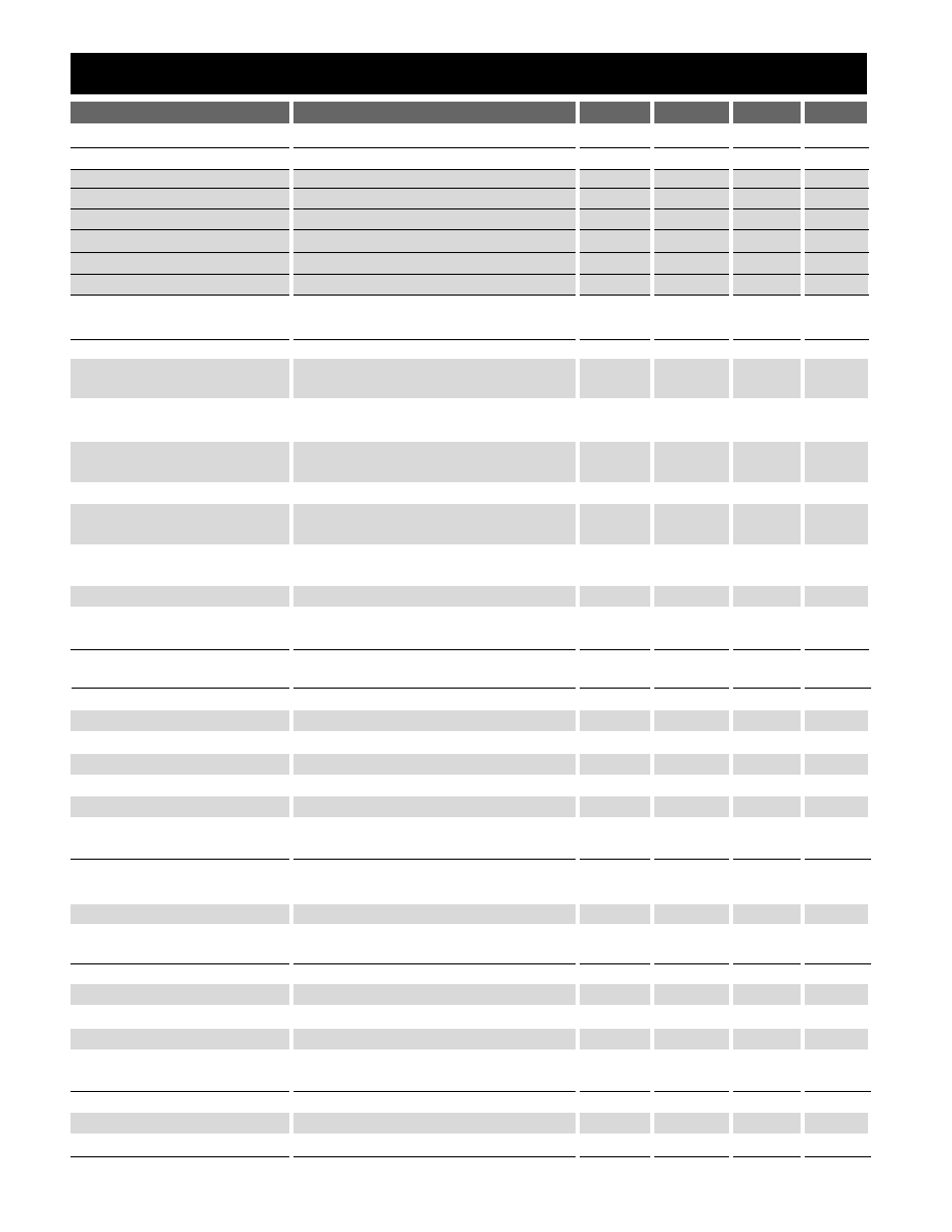
PARAMETER
TEST CONDITIONS
MIN
TYP
MAX
UNIT
CS5150
Electrical Characteristics:
0∞C < T
A
< +70∞C; 0∞C < T
J
< +85∞C; 8V < V
CC1
< 14V; 5V < V
CC2
< 14V; DAC Code: V
ID2
= V
ID1
=
V
ID0
= 1; V
ID3
= 0; CV
GATE(L)
and CV
GATE(H)
= 1nF; C
OFF
= 330pF; C
SS
= 0.1µF, unless otherwise specified.
Absolute Maximum Ratings
s
Error Amplifier
V
FB
Bias Current
V
FB
= 0V
0.3
1.0
µA
Open Loop Gain
1.25V < V
COMP
< 4V; Note 1
50
60
dB
Unity Gain Bandwidth
Note 1
500
3000
kH
COMP SINK Current
V
COMP
= 1.5V; V
FB
= 3V; V
SS
> 2V
0.4
2.5
8.0
mA
COMP SOURCE Current
V
COMP
= 1.2V; V
FB
= 2.7V; V
SS
= 5V
30
50
70
µA
COMP CLAMP Current
V
COMP
= 0V; V
FB
= 2.7V
0.4
1.0
1.6
mA
COMP High Voltage
V
FB
= 2.7V; V
SS
= 5V
4.0
4.3
5.0
V
COMP Low Voltage
V
FB
=3V 160
600
mV
PSRR
8V < V
CC1
< 14V @ 1kHz; Note 1
60
85
dB
s
V
CC1
Monitor
Start Threshold
Output switching
3.75
3.90
4.05
V
Stop Threshold
Output not switching
3.70
3.85
4.00
V
Hysteresis
Start-Stop
50
mV
s
DAC
Input Threshold
V
ID0
, V
ID1
, V
ID2
, V
ID3
1.00
1.25
2.40
V
Input Pull Up Resistance
V
ID0
, V
ID1
, V
ID2
, V
ID3
25
50
100
k
Pull Up Voltage
4.85
5.00
5.15
V
Accuracy
Measure V
FB
= V
COMP
, 25∞C T
J
85∞C
1.0
%
V
ID3
V
ID2
V
ID1
V
ID0
1
1
1
1
1.2315
1.2440
1.2564
V
1
1
1
0
2.1186
2.1400
2.1614
V
1
1
0
1
2.2176
2.2400
2.2624
V
1
1
0
0
2.3166
2.3400
2.3634
V
1
0
1
1
2.4156
2.4400
2.4644
V
1
0
1
0
2.5146
2.5400
2.5654
V
1
0
0
1
2.6136
2.6400
2.6664
V
1
0
0
0
2.7126
2.7400
2.7674
V
0
1
1
1
2.8116
2.8400
2.8684
V
0
1
1
0
2.9106
2.9400
2.9694
V
CS5150
3
PARAMETER
TEST CONDITIONS
MIN
TYP
MAX
UNIT
Electrical Characteristics:
0∞C < T
A
< +70∞C; 0∞C < T
J
< +85∞C; 8V < V
CC1
< 14V; 5V < V
CC2
< 14V; DAC Code: V
ID2
= V
ID1
=
V
ID0
= 1; V
ID3
= 0; CV
GATE(L)
and CV
GATE(H)
= 1nF; C
OFF
= 330pF; C
SS
= 0.1µF, unless otherwise specified.
s
DAC: continued
V
ID3
V
ID2
V
ID1
V
ID0
0
1
0
1
3.0096
3.0400
3.0704
V
0
1
0
0
3.1086
3.1400
3.1714
V
0
0
1
1
3.2076
3.2400
3.2724
V
0
0
1
0
3.3066
3.3400
3.3734
V
0
0
0
1
3.4056
3.4400
3.4744
V
0
0
0
0
3.5046
3.5400
3.5754
V
s
V
GATE(H)
and V
GATE(L)
Out SOURCE Sat at 100mA
Measure V
CC1
≠ V
GATE(L),
;V
CC2
≠ V
GATE(H)
1.2
2.0
V
Out SINK Sat at 100mA
Measure V
GATE(H)
≠ VPGnd;
1.0
1.5
V
V
GATE(L)
≠ VPGnd
Out Rise Time
1V < V
GATE(H)
< 9V; 1V < V
GATE(L)
< 9V
30
50
ns
V
CC1
= V
CC2
= 12V
Out Fall Time
9V > V
GATE(H)
> 1V; 9V > V
GATE(L)
> 1V
30
50
ns
V
CC1
= V
CC2
= 12V
Shoot-Through Current
Note 1
50
mA
Delay V
GATE(H)
to V
GATE(L)
V
GATE(H)
falling to 2V; V
CC1
= V
CC2
= 8V
25
50
ns
V
GATE(L)
rising to 2V
Delay V
GATE(L)
to V
GATE(H)
V
GATE(L)
falling to 2V; V
CC1
= V
CC2
= 8V
25
50
ns
V
GATE(H)
rising to 2V
V
GATE(H)
, V
GATE(L)
Resistance
Resistor to LGnd
20
50
100
k
V
GATE(H)
, V
GATE(L)
Schottky
LGnd to V
GATE(H)
@ 10mA
600
800
mV
LGnd to V
GATE(L)
@ 10mA
s
Soft Start (SS)
Charge Time
1.6
3.3
5.0
ms
Pulse Period
25
100
200
ms
Duty Cycle
(Charge Time/Pulse Period) ◊ 100
1.0
3.3
6.0
%
COMP Clamp Voltage
V
FB
= 0V; V
SS
= 0
0.50
0.95
1.10
V
V
FFB
SS Fault Disable
V
GATE(H)
= Low; V
GATE(L)
= Low
0.9
1.0
1.1
V
High Threshold
2.5
3.0
V
s
PWM Comparator
Transient Response
V
FFB
= 0 to 5V to V
GATE(H)
= 9V to 1V;
100
125
ns
V
CC1
= V
CC2
= 12V
V
FFB
Bias Current
V
FFB
= 0V
0.3
µA
s
Supply Current
I
CC1
No Switching
8.5
13.5
mA
I
CC2
No Switching
1.6
3.0
mA
Operating I
CC1
V
FB
= COMP = V
FFB
8
13
mA
Operating I
CC2
V
FB
= COMP = V
FFB
2
5
mA
s
C
OFF
Normal Charge Time
V
FFB
= 1.5V; V
SS
= 5V
1.0
1.6
2.2
µs
Extension Charge Time
V
SS
= V
FFB
= 0
5.0
8.0
11.0
µs
Discharge Current
C
OFF
to 5V; V
FB
>1V
5.0
mA

PARAMETER
TEST CONDITIONS
MIN
TYP
MAX
UNIT
4
CS5150
Package Pin Description
PACKAGE PIN #
PIN SYMBOL
FUNCTION
Electrical Characteristics:
0∞C < T
A
< +70∞C; 0∞C < T
J
< +85∞C; 8V < V
CC1
< 14V; 5V < V
CC2
< 14V; DAC Code: V
ID2
= V
ID1
=
V
ID0
= 1; V
ID3
= 0; CV
GATE(L)
and CV
GATE(H)
= 1nF; C
OFF
= 330pF; C
SS
= 0.1µF, unless otherwise specified.
s
Time Out Timer
Time Out Time
V
FB
= V
COMP
; V
FFB
= 2V;
10
30
50
µs
Record V
GATE(H)
Pulse High Duration
Fault Mode Duty Cycle
V
FFB
= 0V
35
50
65
%
Note 1: Guaranteed by design, not 100% tested in production.
16L SO Narrow & PDIP
1,2,3,4
V
ID0
≠ V
ID3
Voltage ID DAC input pins. These pins are internally pulled up to 5V
providing logic ones if left open. The DAC range is 2.14V to 3.54V with
100mV increments. V
ID0
- V
ID3
select the desired DAC output voltage.
Leaving all 4 DAC input pins open results in a DAC output voltage of
1.244V, allowing for adjustable output voltage, using a traditional resis-
tor divider.
5
SS
Soft Start Pin. A capacitor from this pin to LGnd in conjunction with
internal 60µA current source provides soft start function for the con-
troller. This pin disables fault detect function during Soft Start. When a
fault is detected, the soft start capacitor is slowly discharged by internal
2µA current source setting the time out before trying to restart the IC.
Charge/discharge current ratio of 30 sets the duty cycle for the IC when
the regulator output is shorted.
6
NC
No connection.
7
C
OFF
A capacitor from this pin to ground sets the time duration for the on
board one shot, which is used for the constant off time architecture.
8
V
FFB
Fast feedback connection to the PWM comparator. This pin is connected
to the regulator output. The inner feedback loop terminates on time.
9
V
CC2
Boosted power for the high side gate driver.
10
V
GATE(H)
High FET driver pin capable of 1.5A peak switching current. Internal cir-
cuit prevents V
GATE(H)
and V
GATE(L)
from being in high state simultane-
ously.
11
PGnd
High current ground for the IC. The MOSFET drivers are referenced to
this pin. Input capacitor ground and the source of lower FET should be
tied to this pin.
12
V
GATE(L)
Low FET driver pin capable of 1.5A peak switching current.
13
V
CC1
Input power for the IC and low side gate driver.
14
LGnd
Signal ground for the IC. All control circuits are referenced to this pin.
15
COMP
Error amplifier compensation pin. A capacitor to ground should be pro-
vided externally to compensate the amplifier.
16
V
FB
Error amplifier DC feedback input. This is the master voltage feedback
which sets the output voltage. This pin can be connected directly to the
output or a remote sense trace.

5
CS5150
Block Diagram
Q
V
ID1
V
CC1
SS
COMP
V
FB
V
ID0
LGnd
V
FFB
V
CC2
V
GATE(H)
PGnd
V
GATE(L)
V
ID2
V
ID3
-
+
4 BIT
DAC
C
OFF
Slow Feedback
Maximum
On-Time
Timeout
V
CC1
R
Q
S
COFF
One Shot
PWM
COMP
SS High
Comparator
FAULT
Latch
2.5V
Error
Amplifier
Fast Feedback
-
+
V
CC1
Monitor
Comparator
-
+
-
+
-
+
-
+
VFFB Low
Comparator
PWM
Comparator
SS Low
Comparator
R
Q
S
Q
R
Q
S
2
µ
A
5V
60
µ
A
Normal
Off-Time
Timeout
Extended
Off-Time
Timeout
Time Out
Timer
(30
µ
s)
Edge Triggered
Off-Time
Timeout
3.90V
3.85V
FAULT
FAULT
GATE(H) = ON
GATE(H) = OFF
PGnd
PWM
Latch
1V
0.7V
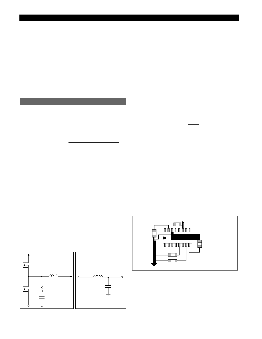
Applications Information
V
2
TM Control Method
The V
2
TM method of control uses a ramp signal that is gen-
erated by the ESR of the output capacitors. This ramp is
proportional to the AC current through the main inductor
and is offset by the value of the DC output voltage. This
control scheme inherently compensates for variation in
either line or load conditions, since the ramp signal is gen-
erated from the output voltage itself. This control scheme
differs from traditional techniques such as voltage mode,
which generates an artificial ramp, and current mode,
which generates a ramp from inductor current.
Figure 1: V
2
TM Control Diagram
The V
2
TM control method is illustrated in Figure 1. The out-
put voltage is used to generate both the error signal and the
ramp signal. Since the ramp signal is simply the output
voltage, it is affected by any change in the output regard-
less of the origin of that change. The ramp signal also con-
tains the DC portion of the output voltage, which allows
the control circuit to drive the main switch to 0% or 100%
duty cycle as required.
A change in line voltage changes the current ramp in the
inductor, affecting the ramp signal, which causes the V
2
TM
control scheme to compensate the duty cycle. Since the
change in inductor current modifies the ramp signal, as in
current mode control, the V
2
TM control scheme has the
same advantages in line transient response.
A change in load current will have an affect on the output
voltage, altering the ramp signal. A load step immediately
changes the state of the comparator output, which controls
the main switch. Load transient response is determined
only by the comparator response time and the transition
speed of the main switch. The reaction time to an output
load step has no relation to the crossover frequency of the
error signal loop, as in traditional control methods.
The error signal loop can have a low crossover frequency,
since transient response is handled by the ramp signal loop.
The main purpose of this `slow' feedback loop is to provide
DC accuracy. Noise immunity is significantly improved,
since the error amplifier bandwidth can be rolled off at a low
frequency. Enhanced noise immunity improves remote sens-
Reference
Voltage
+
C
≠
E
+
≠
Ramp
Signal
Output
Voltage
Feedback
Error
Signal
V
GATE(H)
V
GATE(L)
Error
Amplifier
V
FFB
COMP
V
FB
PWM
Comparator
Theory of Operation

ing of the output voltage, since the noise associated with
long feedback traces can be effectively filtered.
Line and load regulation are drastically improved because
there are two independent voltage loops. A voltage mode
controller relies on a change in the error signal to compen-
sate for a deviation in either line or load voltage. This
change in the error signal causes the output voltage to
change corresponding to the gain of the error amplifier,
which is normally specified as line and load regulation. A
current mode controller maintains fixed error signal under
deviation in the line voltage, since the slope of the ramp
signal changes, but still relies on a change in the error sig-
nal for a deviation in load. The V
2
TM method of control
maintains a fixed error signal for both line and load varia-
tion, since the ramp signal is affected by both line and load.
Constant Off Time
To maximize transient response, the CS5150 uses a constant
off time method to control the rate of output pulses. During
normal operation, the off time of the high side switch is ter-
minated after a fixed period, set by the C
OFF
capacitor. To
maintain regulation, the V
2
TM control loop varies switch on
time. The PWM comparator monitors the output voltage
ramp, and terminates the switch on time.
Constant off time provides a number of advantages. Switch
duty cycle can be adjusted from 0 to 100% on a pulse by
pulse basis when responding to transient conditions. Both
0% and 100% duty cycle operation can be maintained for
extended periods of time in response to load or line tran-
sients. PWM slope compensation to avoid sub-harmonic
oscillations at high duty cycles is avoided.
Switch on time is limited by an internal 30µs timer, mini-
mizing stress to the power components.
Programmable Output
The CS5150 is designed to provide two methods for pro-
gramming the output voltage of the power supply. A four
bit on board digital to analog converter (DAC) is used to
program the output voltage from 2.14V to 3.54V in 100mV
steps, depending on the digital input code. If all four bits
are left open, the CS5150 enters adjust mode. In adjust
mode, the designer can choose any output voltage by using
resistor divider feedback to the V
FB
and V
FFB
pins, as in tra-
ditional controllers. The CS5150 is specifically designed to
be upwards compatible with the CS5155, which uses a five
bit DAC code.
Start Up
Until the voltage on the V
CC1
supply pin exceeds the 3.9V
monitor threshold, the soft start and gate pins are held low.
The FAULT latch is reset (no Fault condition). The output
of the error amplifier (COMP) is pulled up to 1V by the
comparator clamp. When the V
CC1
pin exceeds the monitor
threshold, the GateH output is activated, and the soft start
capacitor begins charging. The GateH output will remain
on, enabling the NFET switch, until terminated by either
the PWM comparator, or the maximum on time timer.
If the maximum on time is exceeded before the regulator
output voltage achieves the 1V level, the pulse is terminat-
ed. The GateH pin drives low, and the GateL pin drives
high for the duration of the extended off time. This time is
set by the time out timer and is approximately equal to the
maximum on time, resulting in a 50% duty cycle. The
GateL pin will then drive low, the GateH pin will drive
high, and the cycle repeats.
When regulator output voltage achieves the 1V level pre-
sent at the COMP pin, regulation has been achieved and
normal off time will ensue. The PWM comparator termi-
nates the switch on time, with off time set by the C
OFF
capacitor. The V
2
TM control loop will adjust switch duty
cycle as required to ensure the regulator output voltage
tracks the output of the error amplifier.
The soft start and COMP capacitors will charge to their
final levels, providing a controlled turn on of the regulator
output. Regulator turn on time is determined by the COMP
capacitor charging to its final value. Its voltage is limited by
the soft start COMP clamp and the voltage on the soft start
pin (see Figures 2 and 3).
Figure 2: CS5150 demonstration board startup in response to increasing
12V and 5V input voltages. Extended off time is followed by normal off
time operation when output voltage achieves regulation to the error
amplifier output.
Figure 3: CS5150 demonstration board startup waveforms.
Trace 1 - Regulator Output Voltage (1V/div.)
Trace 3 - COMP Pin (error amplifier output) (1V/div.)
Trace 4 - Soft Start Pin (2V/div.)
Trace 1 - Regulator Output Voltage (1V/div.)
Trace 2 - Inductor Switching Node (2V/div.)
Trace 3 - 12V input (V
CC1
and V
CC2
) (5V/div.)
Trace 4 - 5V Input (1V/div.)
CS5150
Applications Information: continued
6
CS5150
7
Applications Information: continued
If the input voltage rises quickly, or the regulator output is
enabled externally, output voltage will increase to the level
set by the error amplifier output more rapidly, usually
within a couple of cycles (see Figure 4).
Figure 4: CS5150 demonstration board enable startup waveforms.
Normal Operation
During normal operation, switch off time is constant and
set by the C
OFF
capacitor. Switch on time is adjusted by the
V
2
TM control loop to maintain regulation. This results in
changes in regulator switching frequency, duty cycle, and
output ripple in response to changes in load and line.
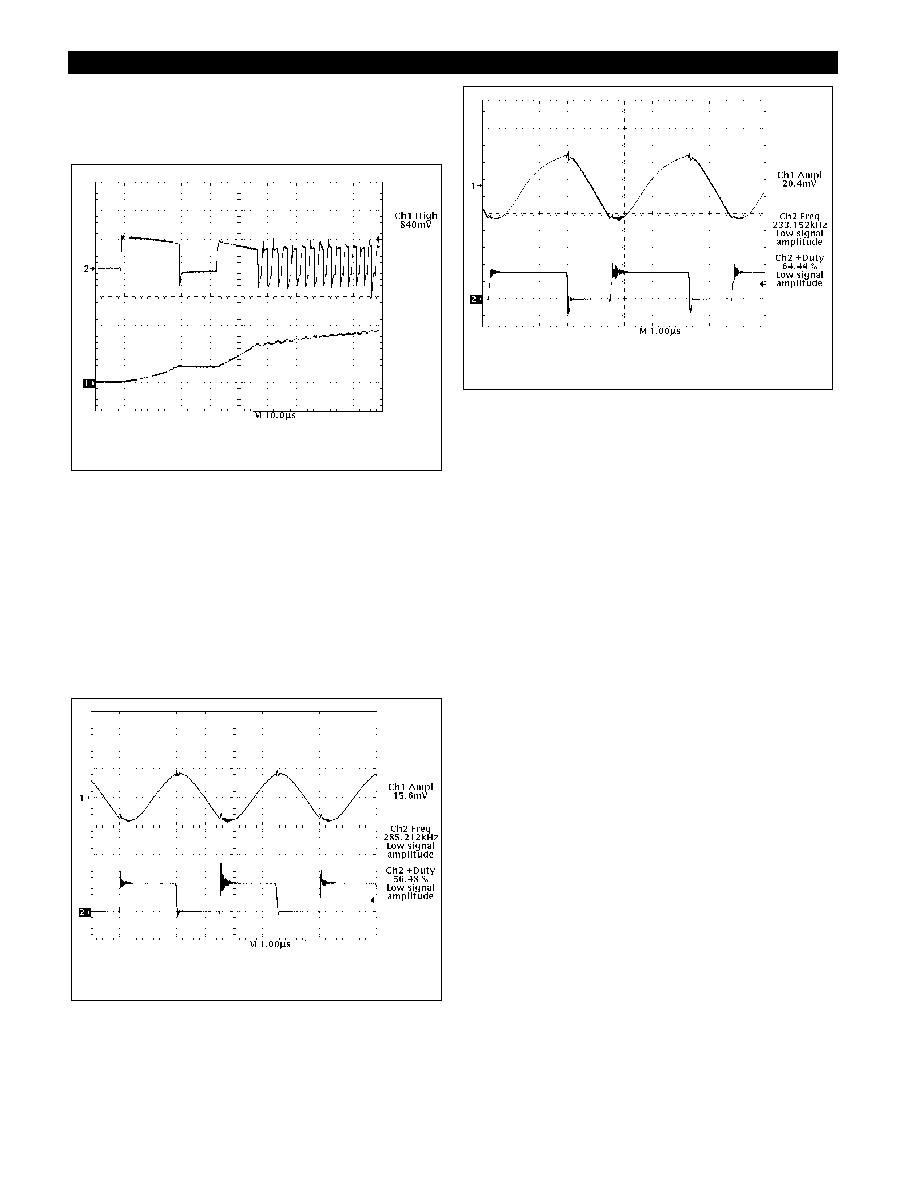
Output voltage ripple will be determined by inductor rip-
ple current working into the ESR of the output capacitors
(see Figures 5 and 6).
Figure 5: Peak-to-peak ripple on V
OUT
= 2.8V, I
OUT
= 0.5A (light load).
Figure 6: Peak-to-peak ripple on V
OUT
= 2.8V, I
OUT
= 13A (heavy load).
Transient Response
The CS5150 V
2
TM control loop's 100ns reaction time pro-
vides unprecedented transient response to changes in
input voltage or output current. Pulse by pulse adjustment
of duty cycle is provided to quickly ramp the inductor cur-
rent to the required level. Since the inductor current cannot
be changed instantaneously, regulation is maintained by
the output capacitor(s) during the time required to slew the
inductor current.
Overall load transient response is further improved
through a feature called "adaptive voltage positioning".
This technique pre-positions the output capacitor's voltage
to reduce total output voltage excursions during changes
in load.
Holding tolerance to 1% allows the error amplifier's refer-
ence voltage to be targeted +40mV high without compro-
mising DC accuracy. A "droop resistor", implemented
through a PC board trace, connects the error amplifier's
feedback pin (V
FB
) to the output capacitors and load and
carries the output current. With no load, there is no DC
drop across this resistor, producing an output voltage
tracking the error amplifier's, including the +40mV offset.
When the full load current is delivered, an 80mV drop is
developed across this resistor. This results in output volt-
age being offset -40mV low.
The result of adaptive voltage positioning is that additional
margin is provided for a load transient before reaching the
output voltage specification limits. When load current sud-
denly increases from its minimum level, the output capaci-
tor is pre-positioned +40mV. Conversely, when load cur-
rent suddenly decreases from its maximum level, the out-
put capacitor is pre-positioned -40mV (see Figures 7, 8, and
9). For best transient response, a combination of a number
of high frequency and bulk output capacitors are usually
used.
Trace1 - Regulator Output Voltage (10V/div.)
Trace 2 - Inductor Switching Node (5V/div.)
Trace 1 - Regulator Output Voltage (10V/div.)
Trace 2 - Inductor Switching Node (5V/div.)
Trace 1 - Regulator Output Voltage (5V/div.)
Trace 2 - Inductor Switching Node (5V/div.)
Applications Information: continued
CS5150
8
If the maximum on time is exceeded while responding to a
sudden increase in load current, a normal off time occurs to
prevent saturation of the output inductor.
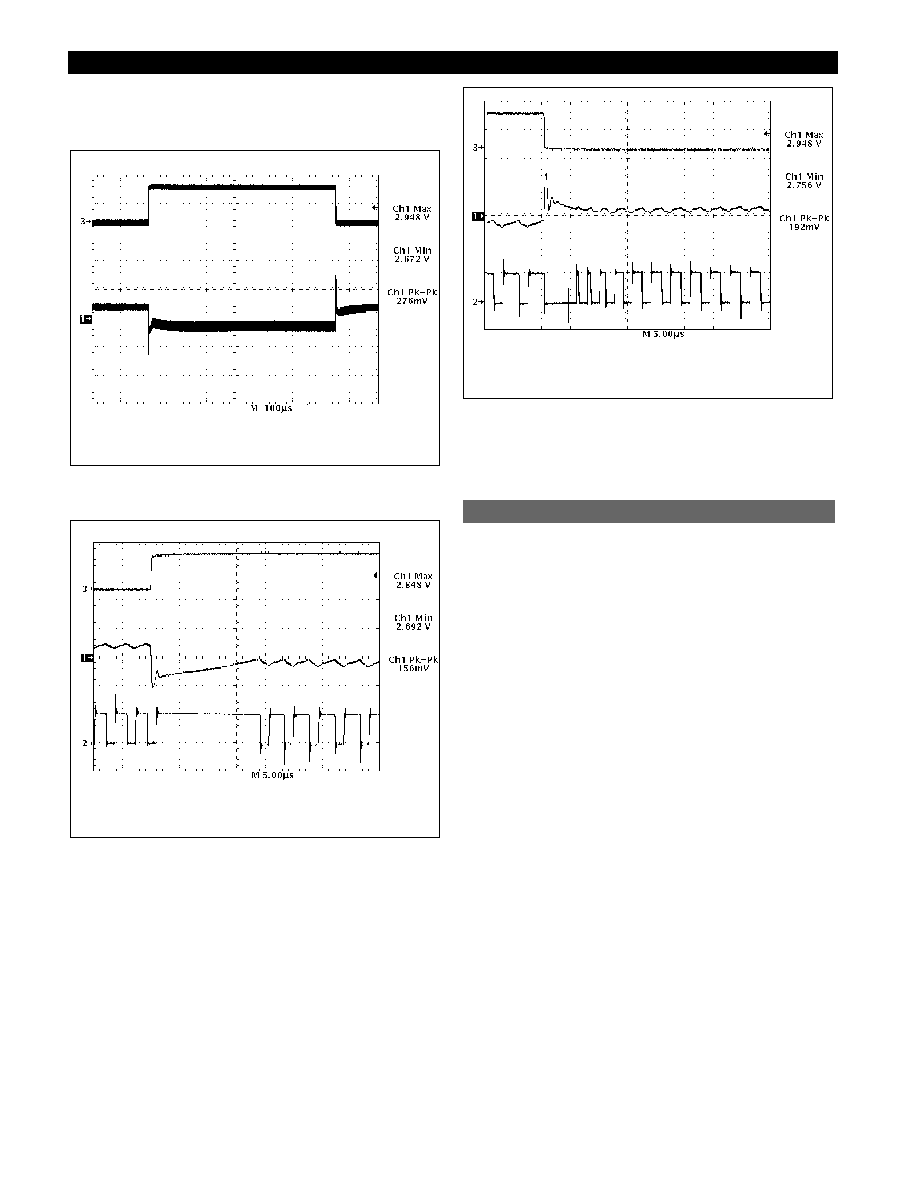
Figure 7: CS5150 demonstration board response to a 0.5 to 13A load
pulse (output set for 2.8V).
Figure 8: CS5150 demonstration board response to 13A load turn on
(output set for 2.8V). Upon completing a normal off time, the V
2
TM con-
trol loop immediately connects the inductor to the input voltage, pro-
viding 100% duty cycle. Regulation is achieved in less than 20µs.
Figure 9: CS5150 demonstration board response to 13A load turn off
(output set for 2.8V). V
2
TM control topology immediately connects
inductor to ground, providing 0% duty cycle. Regulation is achieved in
less than 10µs.
V
CC1
Monitor
To maintain predictable startup and shutdown characteris-
tics an internal V
CC1
monitor circuit is used to prevent the
part from operating below 3.75V minimum startup. The
V
CC1
monitor comparator provides hysteresis and guaran-
tees a 3.70V minimum shutdown threshold.
Short Circuit Protection
A lossless hiccup mode short circuit protection feature is
provided, requiring only the soft start capacitor to imple-
ment. If a short circuit condition occurs (V
FFB
< 1V), the V
FFB
low comparator sets the FAULT latch. This causes the top
MOSFET to shut off, disconnecting the regulator from its
input voltage. The soft start capacitor is then slowly dis-
charged by a 2µA current source until it reaches its lower
0.7V threshold. The regulator will then attempt to restart nor-
mally, operating in its extended off time mode with a 50%
duty cycle, while the soft start capacitor is charged with a
60µA charge current.
If the short circuit condition persists, the regulator output
will not achieve the 1V low V
FFB
comparator threshold
before the soft start capacitor is charged to its upper 2.5V
threshold. If this happens the cycle will repeat itself until the
short is removed. The soft start charge/discharge current
ratio sets the duty cycle for the pulses (2µA/60µA = 3.3%),
while actual duty cycle is half that due to the extended off
time mode (1.65%).
Protection and Monitoring Features
Trace1 - Regulator Output Voltage (1V/div.)
Trace 2 - Inductor Switching Node (5V/div.)
Trace 3 - Output Current (13 to 0.5 Amps) (20V/div.)
Trace 1 - Regulator Output Voltage (1V/div.)
Trace 2 - Inductor Switching Node (5V/div.)
Trace 3 - Output Current (0.5 to 13 Amps) (20V/div.)
Trace 1 - Regulator Output Voltage (1V/div.)
Trace 3 - Regulator Output Current (20V/div.)

CS5150
Applications Information: continued
9
This protection feature results in less stress to the regulator
components, input power supply, and PC board traces
than occurs with constant current limit protection (see
Figures 10 and 11).
If the short circuit condition is removed, output voltage
will rise above the 1V level, preventing the FAULT latch
from being set, allowing normal operation to resume.
Figure 10: CS5150 demonstration board hiccup mode short circuit pro-
tection. Gate pulses are delivered while the soft start capacitor charges,
and cease during discharge.
Figure 11: Startup with regulator output shorted.
Overvoltage Protection
Overvoltage protection (OVP) is provided as result of the
normal operation of the V
2
TM control topology and requires
no additional external components. The control loop
responds to an overvoltage condition within 100ns, causing
the top MOSFET to shut off, disconnecting the regulator
from its input voltage. The bottom MOSFET is then activat-
ed, resulting in a "crowbar" action to clamp the output
voltage and prevent damage to the load (see Figures 12 and
13). The regulator will remain in this state until the over-
voltage condition ceases or the input voltage is pulled low.
The bottom FET and board trace must be properly
designed to implement the OVP function.
Figure 12: OVP response to an input-to-output short circuit by immedi-
ately providing 0% duty cycle, crow-barring the input voltage to
ground.
Figure 13: OVP response to an input-to-output short circuit by pulling
the input voltage to ground.
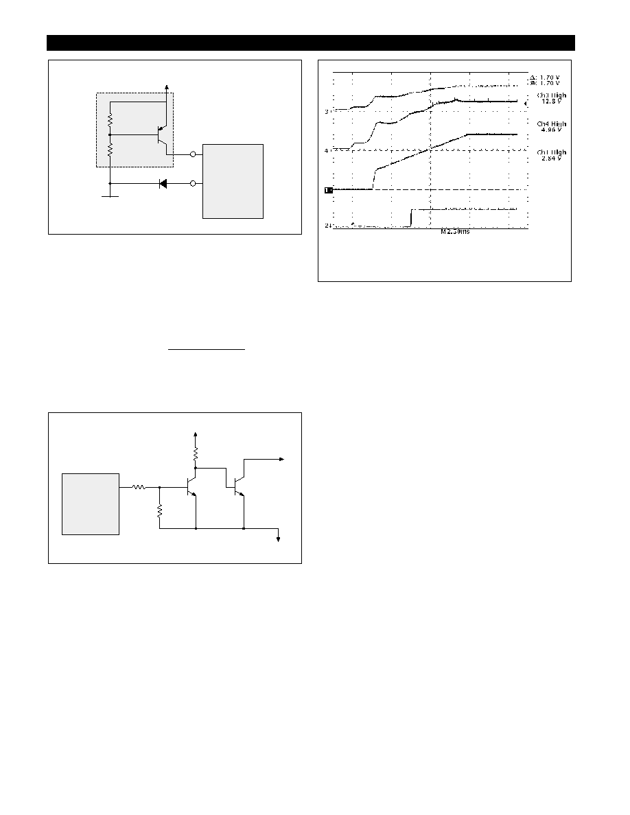
External Output Enable Circuit
On/off control of the regulator can be implemented
through the addition of two additional discrete compo-
nents (see Figure 14). This circuit operates by pulling the
soft start pin high, and the V
FFB
pin low, emulating a short
circuit condition.
Trace 4 = 5V from PC Power Supply (2V/div.)
Trace 1 = Regulator Output Voltage (1V/div.)
Trace 4 = 5V from PC Power Supply (5V/div.)
Trace1 = Regulator Output Voltage (1V/div.)
Trace 2 = Inductor Switching Node (5V/div.)
Trace 4 = 5V from PC Power Supply (2V/div.)
Trace 2 = Inductor Switching Node (2V/div.)
Trace 4 - 5V Supply Voltage (2V/div.)
Trace 3 - Soft Start Timing Capacitor (1V/div.)
Trace 2 - Inductor Switching Node (2V/div.)
Applications Information: continued
CS5150
10
Figure 14: Implementing shutdown with the CS5150.
External Power Good Circuit
An optional Power Good signal can be generated through
the use of four additional external components (see Figure
15). The threshold voltage of the Power Good signal can be
adjusted per the following equation:
V
Power Good
=
This circuit provides an open collector output that drives
the Power Good output to ground for regulator voltages
less than V
Power Good
.
Figure 15: Implementing Power Good with the CS5150.
Figure 16: CS5150 demonstration board during power up. Power Good
signal is activated when output voltage reaches 1.70V.
Selecting External Components
The CS5150 can be used with a wide range of external
power components to optimize the cost and performance of
a particular design. The following information can be used
as general guidelines to assist in their selection.
NFET Power Transistors
Both logic level and standard MOSFETs can be used. The
reference designs derive gate drive from the 12V supply
which is generally available in most computer systems and
utilize logic level MOSFETs. A charge pump may be easily
implemented to support 5V only systems. Multiple
MOSFETs may be paralleled to reduce losses and improve
efficiency and thermal management.
Voltage applied to the MOSFET gates depends on the
application circuit used. Both upper and lower gate driver
outputs are specified to drive to within 1.5V of ground
when in the low state and to within 2V of their respective
bias supplies when in the high state. In practice, the MOS-
FET gates will be driven rail to rail due to overshoot caused
by the capacitive load they present to the controller IC. For
the typical application where V
CC1
= V
CC2
= 12V and 5V is
used as the source for the regulator output current, the fol-
lowing gate drive is provided;
V
GATE(H)
= 12V - 5V = 7V, V
GATE(L)
= 12V (see Figure 17).
Trace 3 = 12V Input (V
CC1
) and V
CC2
) (10V/div.)
Trace 4 = 5V Input (2V/div.)
Trace 1 = Regulator Output Voltage (1V/div.)
Trace 2 = Power Good Signal (2V/div.)
V
OUT
CS5150
R1
10k
R2
6.2k
R3
10k
Power Good
5V
PN3904
PN3904
(R1 + R2) ◊ 0.65V
R2
Shutdown
Input
5V
V
FFB
CS5150
SS
5
8
IN4148
MMUN2111T1 (SOT-23)

CS5150
Applications Information: continued
11
Figure 17: CS5150 gate drive waveforms depicting rail to rail swing.
The most important aspect of MOSFET performance is
RDS
ON
, which effects regulator efficiency and MOSFET
thermal management requirements.
The power dissipated by the MOSFETs may be estimated
as follows;
Switching MOSFET:
Power = I
LOAD
2
◊ RDS
ON
◊ duty cycle
Synchronous MOSFET:
Power = I
LOAD
2
◊ RDSON ◊ (1 - duty cycle)
Duty Cycle =
Off Time Capacitor (C
OFF
)
The C
OFF
timing capacitor sets the regulator off time:
T
OFF
= C
OFF
◊ 4848.5
When the V
FFB
pin is less than 1V, the current charging the
C
OFF
capacitor is reduced. The extended off time can be cal-
culated as follows:
T
OFF
= C
OFF
◊ 24,242.5.
Off time will be determined by either the T
OFF
time, or the
time out timer, whichever is longer.
The preceding equations for duty cycle can also be used to
calculate the regulator switching frequency and select the
C
OFF
timing capacitor:
C
OFF
= ,
where:
Period =
Schottky Diode for Synchronous MOSFET
A Schottky diode may be placed in parallel with the syn-
chronous MOSFET to conduct the inductor current upon
turn off of the switching MOSFET to improve efficiency.
The CS5150 reference circuit does not use this device due to
its excellent design. Instead, the body diode of the syn-
chronous MOSFET is utilized to reduce cost and conducts
the inductor current. For a design operating at 200kHz or so,
the low non-overlap time combined with Schottky forward
recovery time may make the benefits of this device not
worth the additional expense (see Figure 6, channel 2). The
power dissipation in the synchronous MOSFET due to body
diode conduction can be estimated by the following equation:
Power = V
bd
◊ I
LOAD
◊ conduction time ◊ switching frequency
Where V
bd
= the forward drop of the MOSFET body diode.
For the CS5150 demonstration board as shown in Figure 6;
Power = 1.6V ◊ 13A ◊ 100ns ◊ 233kHz = 0.48W
This is only 1.3% of the 36.4W being delivered to the load.
"Droop" Resistor for Adaptive Voltage Positioning
Adaptive voltage positioning is used to reduce output volt-
age excursions during abrupt changes in load current.
Regulator output voltage is offset +40mV when the regula-
tor is unloaded, and -40mV at full load. This results in
increased margin before encountering minimum and maxi-
mum transient voltage limits, allowing use of less capaci-
tance on the regulator output (see Figure 7).
To implement adaptive voltage positioning, a "droop"
resistor must be connected between the output inductor
and output capacitors and load. This is normally imple-
mented by a PC board trace of the following value:
R
DROOP
=
Adaptive voltage positioning can be disabled for improved
DC regulation by connecting the V
FB
pin directly to the load
using a separate, non-load current carrying circuit trace.
80mV
I
MAX
1
switching frequency
Period ◊ (1 - duty cycle)
4848.5
V
OUT
+ (I
LOAD
◊ RDS
ON OF SYNCH FET
)
V
IN
+ (I
LOAD
◊ RDS
ON OF SYNCH FET
) - (I
LOAD
◊ RDS
ON OF SWITCH FET
)
Trace 3 = V
GATE(H)
(10V/div.)
Math 1= V
GATE(H)
- 5V
IN
Trace 4 = V
GATE(L)
(10V/div.)
Trace 2 = Inductor Switching Node (5V/div.)
Applications Information: continued
CS5150
12
Input and Output Capacitors
These components must be selected and placed carefully to
yield optimal results. Capacitors should be chosen to pro-
vide acceptable ripple on the input supply lines and regula-
tor output voltage. Key specifications for input capacitors
are their ripple rating, while ESR is important for output
capacitors. For best transient response, a combination of
low value/high frequency and bulk capacitors placed close
to the load will be required.
Output Inductor
The inductor should be selected based on its inductance,
current capability, and DC resistance. Increasing the induc-
tor value will decrease output voltage ripple, but degrade
transient response.
Thermal Considerations for Power MOSFETs and Diodes
In order to maintain good reliability, the junction tempera-
ture of the semiconductor components should be kept to a
maximum of 150∞C or lower. The thermal impedance (junc-
tion to ambient) required to meet this requirement can be
calculated as follows:
Thermal Impedance =
A heatsink may be added to TO-220 components to reduce
their thermal impedance. A number of PC board layout
techniques such as thermal vias and additional copper foil
area can be used to improve the power handling capability
of surface mount components.
EMI Management
As a consequence of large currents being turned on and off
at high frequency, switching regulators generate noise as a
consequence of their normal operation. When designing for
compliance with EMI/EMC regulations, additional com-
ponents may be added to reduce noise emissions. These
components are not required for regulator operation and
experimental results may allow them to be eliminated. The
input filter inductor may not be required because bulk filter
and bypass capacitors, as well as other loads located on the
board will tend to reduce regulator di/dt effects on the cir-
cuit board and input power supply. Placement of the
power component to minimize routing distance will also
help to reduce emissions.
Figure 18: Filter components
Figure 19: Input Filter
Layout Guidelines
1. Place 12V filter capacitor next to the IC and connect
capacitor ground to pin 11 (PGnd).
2. Connect pin 11 (PGnd) with a separate trace to the
ground terminals of the 5V input capacitors.
3. Place fast feedback filter capacitor next to pin 8 (V
FFB
)
and connect its ground terminal with a separate, wide trace
directly to pin 14 (LGnd).
4. Connect the ground terminals of the Compensation
capacitor directly to the ground of the fast feedback filter
capacitor to prevent common mode noise from effecting
the PWM comparator.
5. Place the output filter capacitor(s) as close to the load as
possible and connect the ground terminal to pin 14 (LGnd).
6. To implement adaptive voltage positioning, connect
both slow and fast feedback pins 16 (V
FB
) and 8 (V
FFB
) to
the regulator output right at the inductor terminal. Connect
inductor to the output capacitors via a trace with the fol-
lowing resistance:
R
TRACE
=
This causes the output voltage to be +40mV with no load,
and -40mV with a full load, improving regulator transient
response. This trace must be wide enough to carry the full
output current. (Typical trace is 1.0 inch long, 0.17 inch
wide). Care should be taken to minimize any additional
losses after the feedback connection point to maximize reg-
ulation.
7. If DC regulation is to be optimized (at the expense of
degraded transient regulation), adaptive voltage position-
ing can be disabled by connecting to V
FB
pin directly to the
load with a separate trace (remote sense).
8. Place 5V input capacitors close to the switching MOSFET
and synchronous MOSFET.
Route gate drive signals V
GATE(H)
(pin 10) and V
GATE(L)
(pin 12 when used) with traces that are a minimum of 0.025
inches wide.
Figure 20: Layout Guidelines
15
To the negative terminal of the
input capacitors
100pF
V
FFB
11
8
OFF TIME
5
SOFTSTART
V
CC
0.1
µ
F
To the negative terminal of the output capacitors
1.0
µ
F
V
COMP
80mV
I
MAX
+
2
µ
H
1200
µ
F x 3/16V
33
1000pF
2
µ
H
T
JUNCTION(MAX)
- T
AMBIENT
Power
Thermal Management
CS5150
13
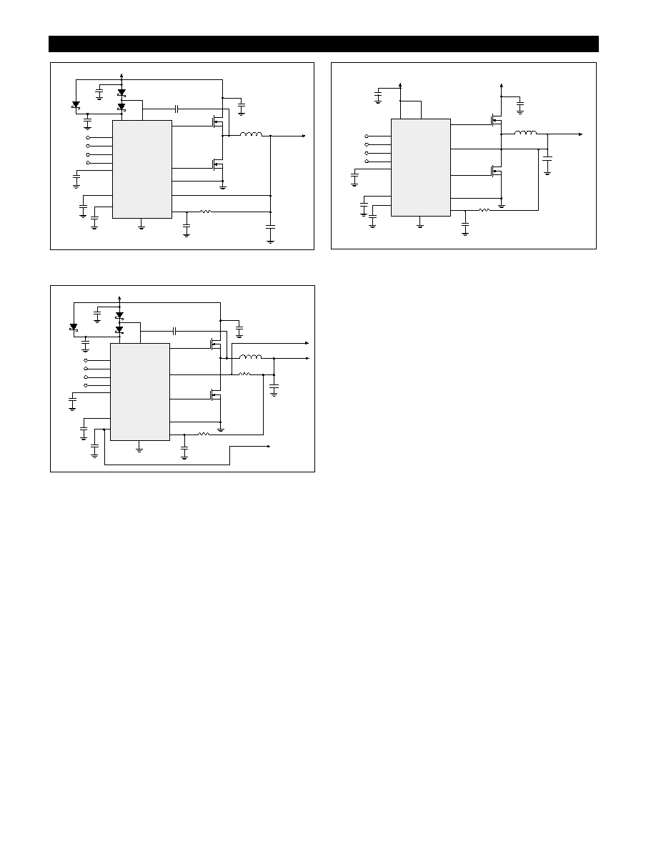
Figure 21: 5V to 3.3V/10A converter.
Figure 22: 5V to 3.3V/10A converter with current sharing.
Figure 23: 3.3V to 2.5V/7A converter with 12V bias.
0.33
µ
F
V
ID0
V
ID1
V
ID2
V
ID3
V
CC1
CS5150
C
OFF
V
FB
V
FFB
COMP
Si9410
Si9410
12V
+
+
5
µ
H
2.5V/7A
V
CC2
PGnd
3.3k
0.1
µ
F
100
µ
F/10V x 2
Tantalum
100pF
330pF
1
µ
F
33
µ
F/25V x 3
Tantalum
3.3V
SS
LGnd
V
GATE(H)
V
GATE(L)
MBRS
120
0.33
µ
F
V
ID0
V
ID1
V
ID2
V
ID3
V
CC1
CS5150
C
OFF
V
FB
V
FFB
COMP
Si9410
Si4410
1
µ
F
5V
+
+
3
µ
H
3.3V/10A
V
CC2
PGnd
3.3k
0.1
µ
F
100
µ
F/10V x 3
Tantalum
100pF
330pF
0.1
µ
F
1
µ
F
MBRS120
MBRS120
100
µ
F/10V x 3
Tantalum
10
Remote
Sense
Connect to
other circuits for
current sharing
SS
LGnd
V
GATE(H)
V
GATE(L)
0.33
µ
F
V
ID0
V
ID1
V
ID2
V
ID3
V
CC1
CS5150
C
OFF
V
FB
V
FFB
COMP
Si9410DY
Si4410DY
1
µ
F
5V
+
+
3
µ
H
3.3V/10A
V
CC2
PGnd
3.3k
0.1
µ
F
100
µ
F/10V x 3
Tantalum
100pF
330pF
0.1
µ
F
1
µ
F
MBRS120
MBRS120
100
µ
F/10V x 3
Tantalum
SS
LGnd
V
GATE(H)
V
GATE(L)
MBRS
120
Additional Application Circuits
14
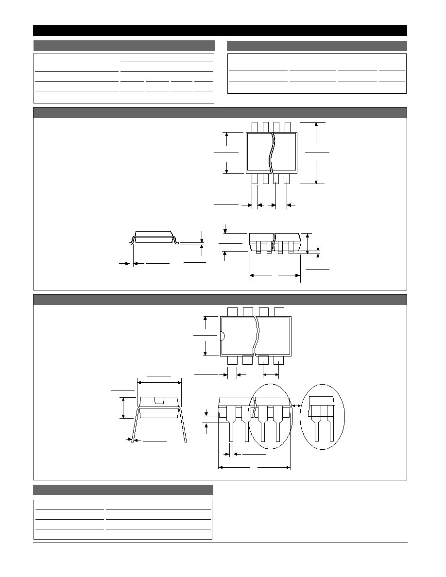
Thermal Data
16L
16L
SO Narrow
PDIP
R
JC
typ
28
42
∞C/W
R
JA
typ
115
80
∞C/W
D
Lead Count
Metric
English
Max
Min
Max
Min
16L SO Narrow
10.00
9.80
.394
.386
16L PDIP
19.69
18.67
.775
.735
CS5150
Package Specification
PACKAGE DIMENSIONS IN mm (INCHES)
PACKAGE THERMAL DATA
Rev. 1/4/99
Ordering Information
Part Number
Description
CS5150GD16
16L SO Narrow
CS5150GDR16
16L SO Narrow (tape & reel)
CS5150GN16
16L PDIP
© 1999 Cherry Semiconductor Corporation
Cherry Semiconductor Corporation reserves the
right to make changes to the specifications without
notice. Please contact Cherry Semiconductor
Corporation for the latest available information.
Surface Mount Narrow Body (D); 150 mil wide
Plastic DIP (N); 300 mil wide
0.39 (.015)
MIN.
2.54 (.100) BSC
1.77 (.070)
1.14 (.045)
D
Some 8 and 16 lead
packages may have
1/2 lead at the end
of the package.
All specs are the same.
.203 (.008)
.356 (.014)
REF: JEDEC MS-001
3.68 (.145)
2.92 (.115)
8.26 (.325)
7.62 (.300)
7.11 (.280)
6.10 (.240)
.356 (.014)
.558 (.022)
1.27 (.050) BSC
0.51 (.020)
0.33 (.013)
6.20 (.244)
5.80 (.228)
4.00 (.157)
3.80 (.150)
1.57 (.062)
1.37 (.054)
D
0.25 (0.10)
0.10 (.004)
1.75 (.069) MAX
1.27 (.050)
0.40 (.016)
REF: JEDEC MS-012
0.25 (.010)
0.19 (.008)