1
V
ID0
PWRGD
V
ID1
V
ID4
V
ID3
V
ID4
V
ID3
V
ID2
COMP
12V
5V
1.2µH
GATE(H)
GATE(L)
PGnd
1200µF/10V x 3
1µF
SS
LGnd
330pF
0.1µF
V
ID0
1200µF
10V x 5
V
ID2
V
ID1
PentiumÆ II
System
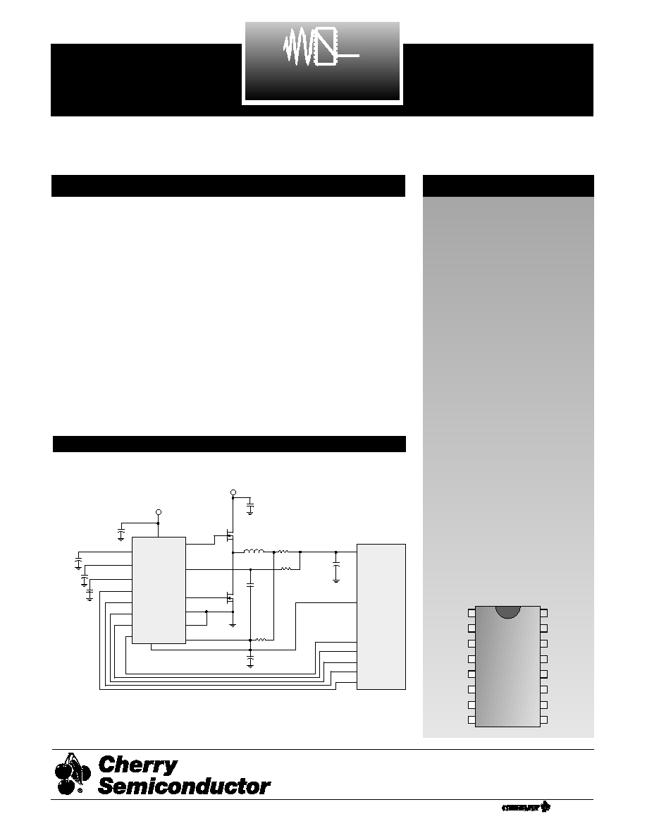
CS5166
V
FB
C
OFF
V
CC
PWRGD
I
SENSE
3.0m
1000pF
510
3.3K
0.1µF
0.1µF
Features
s
V
2
TM
Control Topology
s
Dual N-Channel Design
s
125ns Controller Transient Response
s
Excess of 1Mhz Operation
s
5-bit DAC with 1% Tolerance
s
Power-Good Output with Internal
Delay
s
Adjustable Hiccup Mode Over
Current Protection
s
Complete Pentium
Æ
II System
Requires just 21 Components
s
5V and 12V Operation
s
Adaptive Voltage Positioning
s
Remote Sense Capability
s
Current Sharing Capability
s
V
CC
Monitor
s
Overvoltage Protection (OVP)
s
Programmable Soft Start
s
200ns PWM Blanking
s
65ns FET Non-Overlap
s
40ns Gate Rise and Fall Times
(3.3nF load)
Package Options
CS5166
5-Bit Synchronous CPU Controller
with Power-Good and Current Limit
CS5166
Description
The CS5166 is a synchronous
dual NFET Buck Regulator
Controller. It is designed to pow-
er the core logic of the latest high
performance CPUs. It uses the
V
2
TM
control method to achieve
the fastest possible transient
response and best overall regula-
tion. It incorporates many addi-
tional features required to ensure
the proper operation and protec-
tion of the CPU and power sys-
tem. The CS5166 provides the
industry's most highly integrat-
ed solution, minimizing external
component count, total solution
size, and cost.
The CS5166 is specifically
designed to power Intel's
Pentium
Æ
II processor and
includes the following features:
5-bit DAC with 1% tolerance,
Power-Good output, adjustable
hiccup mode over-current pro-
tection, V
CC
monitor, Soft Start,
adaptive voltage positioning,
over-voltage protection, remote
sense and current sharing capa-
bility.
The CS5166 will operate over a
4.15 to 14V range and is available
in a 16 lead wide body surface
mount package.
Application Diagram
1
16 Lead SO WIDE
A Company
Æ
V
ID0
V
ID1
V
ID2
V
ID3
I
SENSE
C
OFF
SS
V
ID4
V
FB
COMP
LGnd
PWRGD
GATE(L)
PGnd
GATE(H)
V
CC
Pentium is a registered trademark of Intel Corporation.
5V to 2.8V @ 14.2A for 300MHz PentiumÆ II
V
2
is a trademark of Switch Power, Inc.
Rev. 6/28/99
Cherry Semiconductor Corporation
2000 South County Trail, East Greenwich, RI 02818
Tel: (401)885-3600 Fax: (401)885-5786
Email: info@cherry-semi.com
Web Site: www.cherry-semi.com

Absolute Maximum Ratings
Pin Symbol
Pin Name
V
MAX
V
MIN
I
SOURCE
I
SINK
2
PACKAGE PIN #
PIN SYMBOL
FUNCTION
Package Pin Description
CS5166
V
CC
IC Power Input
16V
-0.3V
N/A
1.5A Peak 200mA DC
SS
Soft Start Capacitor
6V
-0.3V
200µA
10µA
COMP
Compensation Capacitor
6V
-0.3V
10mA
1mA
V
FB
Voltage Feedback and Current
6V
-0.3V
1mA
1mA
Sense Comparator Input
C
OFF
Off-Time Capacitor
6V
-0.3V
1mA
50mA
V
ID0-4
Voltage ID DAC Inputs
6V
-0.3V
1mA
10µA
GATE(H)
High-Side FET Driver
16V
-0.3V
1.5A Peak
1.5A Peak
200mA DC
200mA DC
GATE(L)
Low-Side FET Driver
16V
-0.3V
1.5A Peak
1.5A Peak
200mA DC
200mA DC
I
SENSE
Current Sense Comparator Input
6V
-0.3V
1mA
1mA
PWRGD
Power-Good Output
6V
-0.3V
10µA
30mA
PGnd
Power Ground
0V
0V
1.5A Peak
N/A
200mA DC
LGnd
Logic Ground
0V
0V
100mA
N/A
1,2,3,4,6
V
IDO
≠ V
ID4
Voltage ID DAC inputs. These pins are internally pulled up to 5V if left
open. V
ID4
selects the DAC range. When V
ID4
is high (logic one), the
Error Amp reference range is 2.125V to 3.525V with 100mV increments.
When V
ID4
is low (logic zero), the Error amp reference voltage is 1.325V
to 2.075V with 50mV increments.
5
SS
Soft Start Pin. A capacitor from this pin to LGnd sets the Soft Start and
fault timing.
7
C
OFF
Off-Time Capacitor Pin. A capacitor from this pin to LGnd sets both the
normal and extended off time.
8
I
SENSE
Current Sense Comparator Inverting Input
9
V
CC
Input Power Supply Pin.
10
GATE(H)
High Side Switch FET driver pin.
11
PGnd
High Current ground for the GATE(H) and GATE(L) pins.
12
GATE(L)
Low Side Synchronous FET driver pin.
13
PWRGD
Power-Good Output. Open collector output drives low when V
FB
is out
of regulation.
14
LGnd
Reference ground. All control circuits are referenced to this pin.
15
COMP
Error Amp output. PWM Comparator reference input. A capacitor to
LGnd provides Error Amp compensation.
16
V
FB
Error Amp, PWM Comparator feedback input, Current Sense
Comparator Non-Inverting input, and PWRGD comparator input.
Operating Junction Temperature, T
J
. . . . . . . . . . . . . . . . . . . . . . . . . . . . . . . . . . . . . . . . . . . . . . . . . . . . . . . . . . . . . 0∞ to 150∞C
Lead Temperature Soldering:
Reflow (SMD styles only) . . . . . . . . . . . . . . . . . . . . . . . . . . . . . . . . . . . . . . . . . . 60 Sec max. above 183∞C, 230∞C Peak
Storage Temperature Range, T
S
. . . . . . . . . . . . . . . . . . . . . . . . . . . . . . . . . . . . . . . . . . . . . . . . . . . . . . . . . . . . . . . -65∞ to 150∞C