1
Features
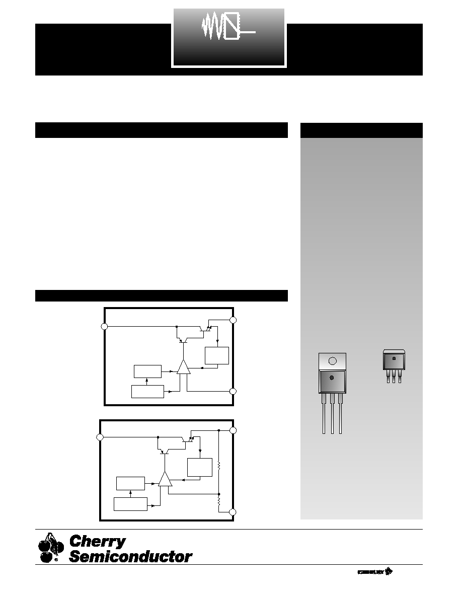
Error
Amplifier
+
Output
Current
Limit
-
V
IN
V
OUT
Adj
Thermal
Shutdown
Bandgap
Error
Amplifier
+
Output
Current
Limit
-
V
IN
V
OUT
Thermal
Shutdown
Bandgap
Gnd
s
Output Current to 6A
s
Output Trimmed to +/- 1%
s
Dropout Voltage
1.3V @ 6A
s
Fast Transient Response
s
Fault Protection Circuitry
Thermal Shutdown
Overcurrent Protection
Safe Area Protection
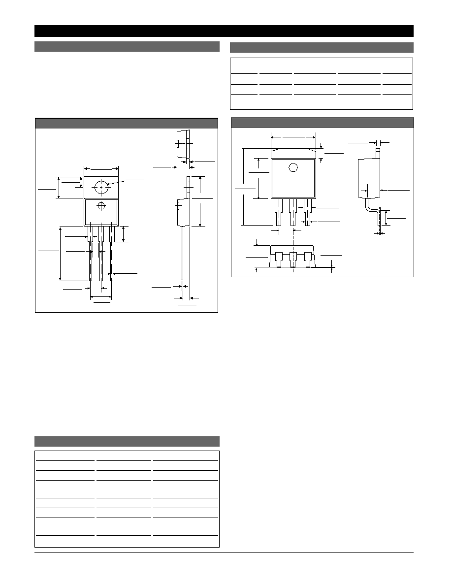
Package Options
3L TO-220
Tab (V
OUT
)
CS5206 -1,-3,-5
6A Adjustable, and Fixed 3.3V
and 5V Linear Regulators
1
CS5206 -1,-3,-5
The CS5206 -X series of linear regu-
lators provides 6A at adjustable
and fixed voltages of 3.3V and 5V
with an accuracy of ±1% and ±2%
respectively. The adjustable version
uses two external resistors to set
the output voltage within a 1.25V
to 13V range.
The regulators are intended for use
as post regulators and microproces-
sor supplies. The fast loop response
and low dropout voltage make
these regulators ideal for applica-
tions where low voltage operation
and good transient response are
important.
The circuit is designed to operate
with dropout voltages as low as 1V
depending on the output current
level. The maximum quiescent cur-
rent is only 10mA at full load.
The regulators are fully protected
against overload conditions with
protection circuitry for Safe
Operating Area (SOA), overcurrent
and thermal shutdown.
The regulators are available in TO-
220 and surface mount D
2
packages.
Block Diagram
CS5206 -3, -5
1
Gnd
2
V
OUT
3
V
IN
CS5206 -1
1
Adj
2
V
OUT
3
V
IN
CS5206 -1
CS5206 -3, -5
Description
3L D
2
PAK
1
Rev. 7/8/97
Cherry Semiconductor Corporation
2000 South County Trail, East Greenwich, RI 02818
Tel: (401)885-3600 Fax: (401)885-5786
Email: info@cherry-semi.com
Web Site: www.cherry-semi.com
A Company
®
2
Electrical Characteristics:
C
IN
= 10µF, C
OUT
= 22µF Tantalum, V
IN
– V
OUT
=3V, V
IN
≤ 10V, 0°C ≤ T
A
≤ 70°C, T
J
≤ +150°C,
unless otherwise specified, I
full load
= 6A.
PARAMETER
TEST CONDITIONS
MIN
TYP
MAX
UNIT
CS5206 -1,-3,-5
Absolute Maximum Ratings
Supply Voltage, V
CC
..................................................................................................................................................................17V
Operating Temperature Range................................................................................................................................-40°C to 70°C
Junction Temperature ............................................................................................................................................................150°C
Storage Temperature Range ..................................................................................................................................-60°C to 150°C
Lead Temperature Soldering: Wave Solder (through hole styles only)..........................................10 sec. max, 260°C peak
Reflow (SMD styles only) ......................................................................................60 sec. max above 183°C, 230°C peak
Electrical Characteristics:
C
IN
= 10µF, C
OUT
= 22µF Tantalum, V
IN
– V
OUT
=3V, V
IN
≤ 15V, 0°C ≤ T
A
≤ 70°C, T
J
≤ +150°C,
unless otherwise specified, I
full load
= 6A.
PARAMETER
TEST CONDITIONS
MIN
TYP
MAX
UNIT
s Fixed Output Voltage (CS5206 -3, -5)
CS5206 -5
V
IN
–V
OUT
= 1.5V;
4.9
5.0
5.1
V
(Notes 1 and 2)
0≤I
OU T
≤6A
(-2%)
(+2%)
CS5206 -3
V
IN
–V
OUT
= 1.5V;
3.234
3.300
3.366
V
(Notes 1 and 2)
0≤I
OUT
≤6A
(-2%)
(+2%)
Line Regulation
1.5V≤V
IN
–V
OUT
≤ 6V; I
OUT
=10mA
0.04
0.20
%
Load Regulation
V
IN
–V
OUT
= 1.5V;
0.1
0.4
%
(Notes 1 and 2)
10mA ≤ I
OUT
≤6A
Dropout Voltage (Note 3)
I
OUT
=6A
1.3
1.4
V
Current Limit
V
IN
–V
OUT
=3V; T
J
≥ 25°C
6.5
8.5
A
V
IN
–V
OUT
=9V
1.0
A
Quiescent Current
V
IN
≤9V; I
OUT
=10mA
5.0
10.0
mA
Thermal Regulation
30ms pulse; T
A
=25°C
0.003
%/W
Ripple Rejection
f=120Hz; I
OUT
=6A
75
dB
Temperature Stability
0.5
%
s Adjustable Output Voltage (CS5206 -1)
Reference Voltage
V
IN
–V
OUT
= 1.5V; V
Adj
= 0V
1.241
1.254
1.266
V
(Notes 1 and 2)
10mA≤I
OUT
≤6A
(-1%)
(+1%)
Line Regulation
1.5V≤V
IN
–V
OUT
≤6V; I
OUT
=10mA
0.04
0.20
%
Load Regulation
V
IN
–V
OUT
=1.5V;
0.1
0.4
%
(Notes 1 and 2)
10mA≤I
OUT
≤6A
Dropout Voltage (Note 3)
I
OUT
=6A
1.3
1.4
V
Current Limit
V
IN
–V
OUT
=3V; T
J
≥ 25°C
6.5
8.5
A
V
IN
–V
OUT
=9V
1.0
A
Minimum Load Current
V
IN
–V
OUT
=7V
1.2
6
mA
Adjust Pin Current
50
100
µA
Adjust Pin Current Change
1.5V≤V
IN
–V
OUT
≤4V; 0.2
5.0
µA
10mA≤I
OUT
≤6A
Thermal Regulation
30ms pulse; T
A
=25°C
0.003
%W
Ripple Rejection
f=120Hz; C
Adj
=25µF; I
OUT
=6A
82
dB
Temperature Stability
0.5
%
RMS Output Noise
10Hz≤f≤10kHz; T
A
=25°C
0.003
%V
OUT
Thermal Shutdown
150
180
°C
Thermal Shutdown Hysteresis
25
°C
CS5206 -1,-3,-5
3
Typical Performance Characteristics
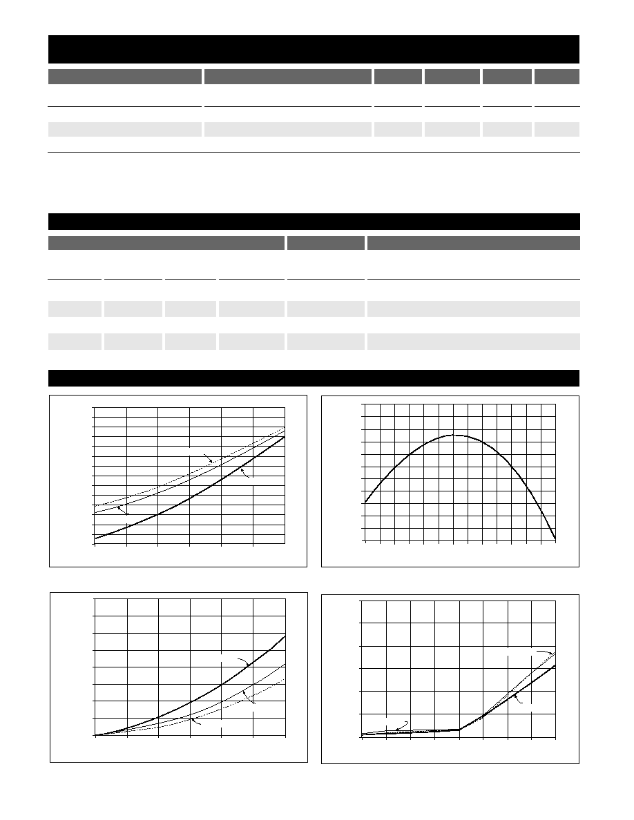
0.85
0.70
0.80
0.90
0.95
1.00
1.05
1.10
1.15
1.20
1.25
1.30
1.35
Dropout V
oltage (V)
Output Current (A)
0.75
1.40
0
1
2
3
4
5
6
T
CASE
= 125
∞C
T
CASE
= 25
∞C
T
CASE
= 0
∞C
0
10
130
-0.12
0.10
Output V
oltage Deviation (%)
T
J
(
∞
C)
20
30
40
50
60
70
80
90 100 110 120
0.08
0.06
0.04
0.02
0.00
-0.02
-0.04
-0.06
-0.08
-0.10
0.025
0.000
0.050
0.075
0.100
0.200
0.125
0.150
0.175
Output Current (A)
Output V
oltage Deviation (%)
0
1
2
3
4
5
6
T
CASE
= 0
∞C
T
CASE
= 125
∞C
T
CASE
= 25
∞C
Dropout Voltage vs. Output Current
Reference Voltage vs. Temperature
Load Regulation vs. Output Current
Package Pin Description
PACKAGE PIN #
PIN SYMBOL
FUNCTION
PARAMETER
TEST CONDITIONS
MIN
TYP
MAX
UNIT
s Fixed Output Voltage (CS5206 -3, -5)
RMS Output Noise (%V
OUT
)
10Hz≤f≤10kHz
0.003
%V
OUT
Thermal Shutdown
150
180
°C
Thermal Shutdown Hysteresis
25
°C
Note 1: Load regulation and output voltage are measured at a constant junction temperature by low duty cycle pulse testing. Changes in out-
put voltage due to thermal gradients or temperature changes must be taken into account separately.
Note 2: Specifications apply for an external Kelvin sense connection at a point on the output pin 1/4” from the bottom of the package.
Note 3: Dropout voltage is a measurement of the minimum input/output differential at full load.
Electrical Characteristics:
C
IN
= 10µF, C
OUT
= 22µF Tantalum, V
IN
– V
OUT
=3V, V
IN
≤ 10V, 0°C ≤ T
A
≤ 70°C, T
J
≤ +150°C,
unless otherwise specified, I
full load
= 6A.
CS5206 -1
CS5206 -3, -5
D
2
PAK
3L TO-220
D
2
PAK
3L TO-220
1
1
N/A
N/A
Adj
Adjust pin (low side of the internal reference).
2
2
2
2
V
OUT
Regulated output voltage (case).
3
3
3
3
V
IN
Input voltage.
N/A
N/A
1
1
Gnd
Ground connection.
1
2
3
4
5
6
0.550
Minimum Load Current (mA)
V
IN
≠ V
OUT
(V)
T
CASE
= 0
∞C
T
CASE
= 125
∞C
7
0.875
1.200
1.525
1.850
2.175
2.500
8
9
T
CASE
= 25
∞C
Minimum Load Current
4
The CS5206 -X family of linear regulators provide fixed or
adjustable voltages at currents up to 6A. The regulators
are protected against short circuit, and include thermal
shutdown and safe area protection (SOA) circuitry. The
SOA protection circuitry decreases the maximum avail-
able output current as the input-output differential volt-
age increases.
The CS5206 -X has a composite PNP-NPN output transistor
and requires an output capacitor for stability. A detailed
procedure for selecting this capacitor is included in the
Stability Considerations section.
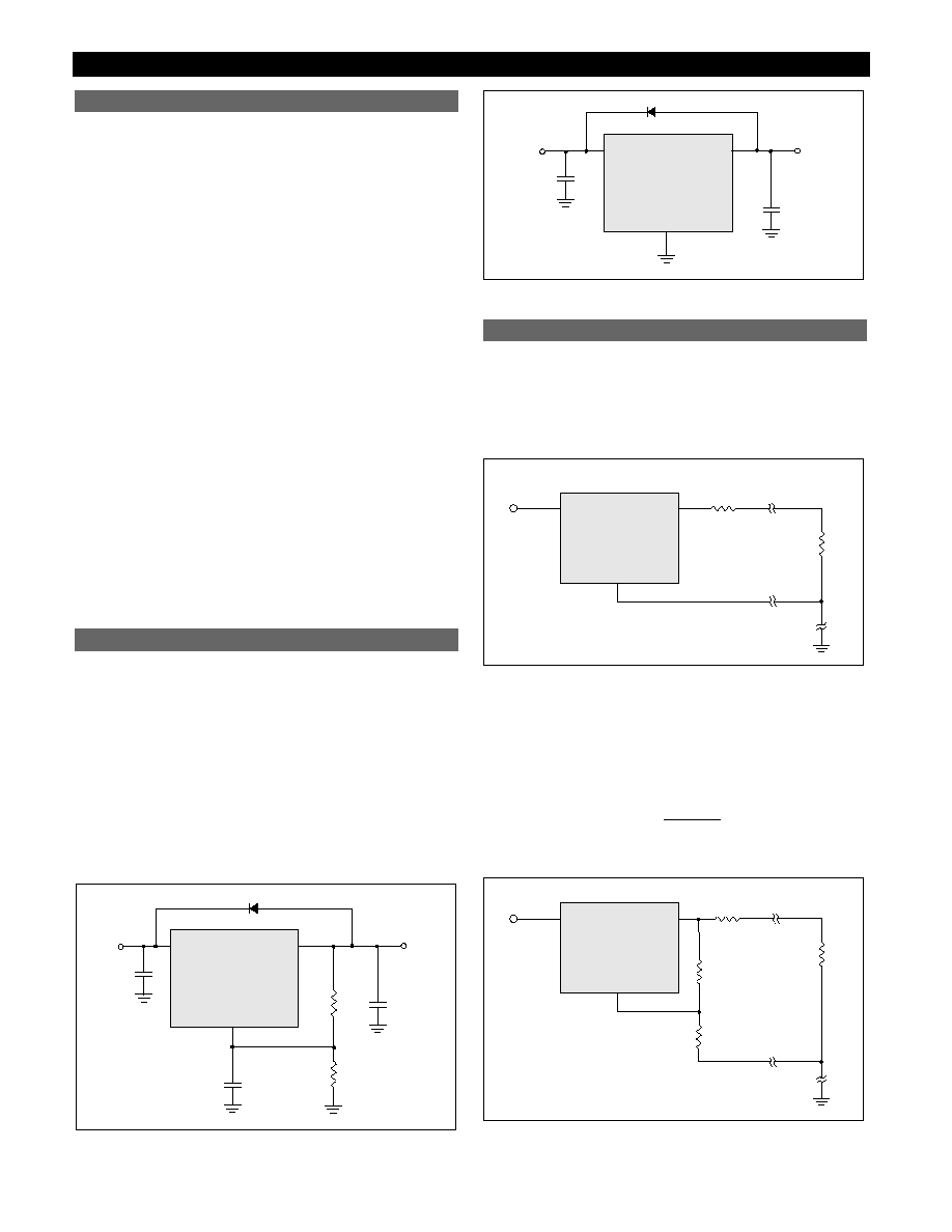
The adjustable regulator (CS5206 -1) has an output voltage
range of 1.25V to 13V. An external resistor divider sets the
output voltage as shown in Figure 1. The regulator main-
tains a fixed 1.25V (typical) reference between the output
pin and the adjust pin.
A resistor divider network R1 and R2 causes a fixed cur-
rent to flow to ground. This current creates a voltage
across R2 that adds to the 1.25V across R1 and sets the
overall output voltage. The adjust pin current (typically
50µA) also flows through R2 and adds a small error that
should be taken into account if precise adjustment of V
OUT
is necessary.
The output voltage is set according to the formula:
V
OUT
= V
REF
¥
(
)
+ I
Adj
¥ R2
The term I
Adj
¥ R2 represents the error added by the adjust
pin current.
R1 is chosen so that the minimum load current is at least
10mA. R1 and R2 should be the same type, e.g. metal film
for best tracking over temperature. The adjust pin is
bypassed to improve the transient response and ripple
rejection of the regulator.
Figure 1. Resistor divider scheme for the adjustable version.
V
OUT
V
IN
CS5206-1
V
IN
Adj
R
1
R
2
C
1
V
OUT
C
2
V
REF
I
Adj
C
Adj
R1 + R2
R1
Adjustable Operation
Applications Information
CS5206 -1,-3,-5
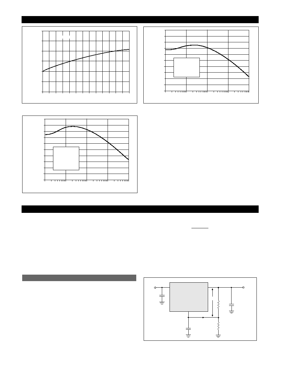
Typical Performance Characteristics: continued
0
20
30
40
50
60
40.0
Adjust Pin Current (
m
A)
Temperature (
∞
C)
80
45.0
50.0
55.0
60.0
65.0
70.0
90
100
10
70
110 120 130
I
O
= 10mA
0.0
10
1
Frequency (Hz)
Ripple Rejection (dB)
10.0
20.0
30.0
40.0
50.0
60.0
70.0
80.0
90.0
100.0
10
2
10
3
10
4
10
5
T
CASE
= 25
∞C
I
OUT
= 6A
(V
IN
– V
OUT
) = 3V
V
RIPPLE
= 1.6V
PP
0.0
10
1
Frequency (Hz)
Ripple Rejection (dB)
10.0
20.0
30.0
40.0
50.0
60.0
70.0
80.0
90.0
100.0
10
2
10
3
10
4
10
5
T
CASE
= 25
∞C
I
OUT
= 6A
(V
IN
– V
OUT
) = 3V
V
RIPPLE
= 1.6V
PP
C
Adj
= 25
mF
Adjust Pin Current vs. Temperature
Ripple Rejection vs. Frequency (Fixed Versions)
Ripple Rejection vs. Frequency (Adjustable Version)
5
The output or compensation capacitor helps determine
three main characteristics of a linear regulator: start-up
delay, load transient response and loop stability.
The capacitor value and type is based on cost, availability,
size and temperature constraints. A tantalum or aluminum
electrolytic capacitor is best, since a film or ceramic capaci-
tor with almost zero ESR, can cause instability. The alu-
minum electrolytic capacitor is the least expensive solu-
tion. However, when the circuit operates at low tempera-
tures, both the value and ESR of the capacitor will vary
considerably. The capacitor manufacturers data sheet pro-
vides this information.
A 22µF tantalum capacitor will work for most applications,
but with high current regulators such as the CS5206 -X the
transient response and stability improve with higher val-
ues of capacitor. The majority of applications for this regu-
lator involve large changes in load current so the output
capacitor must supply the instantaneous load current. The
ESR of the output capacitor causes an immediate drop in
output voltage given by:
∆V = ∆I
¥ ESR
For microprocessor applications it is customary to use an
output capacitor network consisting of several tantalum
and ceramic capacitors in parallel. This reduces the overall
ESR and reduces the instantaneous output voltage drop
under load transient conditions. The output capacitor net-
work should be as close as possible to the load for the best
results.
When large external capacitors are used with a linear regu-
lator it is sometimes necessary to add protection diodes. If
the input voltage of the regulator gets shorted, the output
capacitor will discharge into the output of the regulator.
The discharge current depends on the value of the capaci-
tor, the output voltage and the rate at which V
IN
drops. In
the CS5206-X family of linear regulators, the discharge
path is through a large junction and protection diodes are
not usually needed. If the regulator is used with large
values of output capacitance and the input voltage is
instantaneously shorted to ground, damage can occur. In
this case, a diode connected as shown in Figures 2a and 2b
is recommended.
Figure 2a. Protection diode scheme for adjustable output regulator.
Figure 2b. Protection diode scheme for fixed output regulators.
Since the CS5206 -X is a three terminal regulator, it is not
possible to provide true remote load sensing. Load regula-
tion is limited by the resistance of the conductors connect-
ing the regulator to the load. For best results the fixed reg-
ulators should be connected as shown in Figure 3.
Figure 3. Conductor parasitic resistance can be minimized with the
above grounding scheme for fixed output regulators.
For the adjustable regulator, the best load regulation
occurs when R1 is connected directly to the output pin of
the regulator as shown in Figure 4. If R1 is connected to the
load, R
C
is multiplied by the divider ratio and the effective
resistance between the regulator and the load becomes
R
C
¥
(
)
R
C
= conductor parasitic resistance
Figure 4. Grounding scheme for the adjustable output regulator to min-
imize parasitics.
V
OUT
R
C
V
IN
conductor parasitic
resistance
CS5206-1
V
IN
Adj
R
LOAD
R
1
R
2
R1 + R2
R1
V
OUT
R
C
V
IN
conductor parasitic
resistance
CS5206-X
V
IN
Gnd
R
LOAD
Output Voltage Sensing
V
OUT
V
IN
CS5206-X
V
IN
Gnd
V
OUT
C
2
C
1
IN4002 (optional)
V
OUT
V
IN
CS5206-1
V
IN
Adj
R
1
R
2
C
1
V
OUT
C
2
C
Adj
IN4002 (optional)
Protection Diodes
Stability Considerations
Applications Information: continued
CS5206-1,-3,-5

6
Applications Information: continued
CS5206 -1,-3,-5
The CS5206 -X series of linear regulators includes thermal
shutdown and safe operating area circuitry to protect the
device. High power regulators such as these usually oper-
ate at high junction temperatures so it is important to cal-
culate the power dissipation and junction temperatures
accurately to ensure that an adequate heat sink is used.
The case is connected to V
OUT
on the CS5206 -X, electrical
isolation may be required for some applications. Thermal
compound should always be used with high current regu-
lators such as these.
The thermal characteristics of an IC depend on the follow-
ing four factors:
1. Maximum Ambient Temperature T
A
(°C)
2. Power dissipation P
D
(Watts)
3. Maximum junction temperature T
J
(°C)
4. Thermal resistance junction to ambient R
QJA
(C/W)
These four are related by the equation
T
J
= T
A
+ P
D
¥ R
QJA
(1)
The maximum ambient temperature and the power dissi-
pation are determined by the design while the maximum
junction temperature and the thermal resistance depend
on the manufacturer and the package type.
The maximum power dissipation for a regulator is:
P
D(max)
={V
IN(max)
–V
OUT(min)
}I
OUT(max)
+V
IN(max)
I
Q
(2)
where
V
IN(max)
is the maximum input voltage,
V
OUT(min)
is the minimum output voltage,
I
OUT(max)
is the maximum output current, for the application
I
Q
is the maximum quiescent current at I
OUT
(max).
A heat sink effectively increases the surface area of the
package to improve the flow of heat away from the IC and
into the surrounding air.
Each material in the heat flow path between the IC and the
outside environment has a thermal resistance. Like series
electrical resistances, these resistances are summed to
determine R
QJA
, the total thermal resistance between the
junction and the surrounding air.
1. Thermal Resistance of the junction to case, R
QJC
(°C/W)
2. Thermal Resistance of the case to Heat Sink, R
QCS
(°C/W)
3. Thermal Resistance of the Heat Sink to the ambient air,
R
QSA
(°C/W)
These are connected by the equation:
R
QJA
= R
QJC
+ R
QCS
+ R
QSA
(3)
The value for R
QJA
is calculated using equation (3) and the
result can be substituted in equation (1).
The value for R
QJC
is normally quoted as a single figure for
a given package type based on an average die size. For a
high current regulator such as the CS5206 -X the majority
of the heat is generated in the power transistor section.
The value for R
QSA
depends on the heat sink type, while
R
QCS
depends on factors such as package type, heat sink
interface (is an insulator and thermal grease used?), and
the contact area between the heat sink and the package.
Once these calculations are complete, the maximum per-
missible value of R
QJA
can be calculated and the proper
heat sink selected. For further discussion on heat sink
selection, see application note “Thermal Management for
Linear Regulators.”
Calculating Power Dissipation and Heat Sink Requirements
7
Part Number
Type
Description
CS5206 -1GT3
6A, adj. output
3 L TO-220 Straight
CS5206 -1GDP3
6A, adj. output
3 L D
2
PAK
CS5206 -1GDPR3
6A, adj. output
3 L D
2
PAK
(tape & reel)
CS5206 -3GT3
6A, 3.3V output 3 L TO-220 Straight
CS5206 -3GDP3
6A, 3.3V output 3 L D
2
PAK
CS5206 -3GDPR3
6A, 3.3V output 3 L D
2
PAK
(tape & reel)
CS5206 -5GT3
6A, 5V output
3 L TO-220 Straight
Ordering Information
Rev. 7/8/97
Package Specification
PACKAGE DIMENSIONS IN mm(INCHES)
Thermal Data
3L
3L
TO-220
D
2
PAK
R
Q
JC
typ
1.6
1.6
˚C/W
R
Q
JA
typ
50
10 - 50*
˚C/W
*Depending on thermal properties of substrate. R
QJA
= R
QJC
+ R
QCA
PACKAGE THERMAL DATA
CS5206 -1,-3,-5
© 1999 Cherry Semiconductor Corporation
Cherry Semiconductor Corporation reserves the
right to make changes to the specifications without
notice. Please contact Cherry Semiconductor
Corporation for the latest available information.
3 Lead D
2
PAK (DP)
2.54 (.100) REF
10.31 (.406)
10.05 (.396)
8.53 (.336)
8.28 (.326)
0.91 (.036)
0.66 (.026)
1.40 (.055)
1.14 (.045)
4.57 (.180)
4.31 (.170)
1.68 (.066)
1.40 (.055)
2.74(.108)
2.49(.098)
1.40 (.055)
1.14 (.045)
0.10 (.004)
0.00 (.000)
.254 (.010) REF
15.75 (.620)
14.73 (.580)
2.79 (.110)
2.29 (.090)
3 Lead TO-220 (T) Straight
5.33 (.210)
4.83 (.190)
2.79 (.110)
2.29 (.090)
1.02 (.040)
0.63 (.025)
0.56 (.022)
0.38 (.014)
1.40 (.055)
1.14 (.045)
4.83 (.190)
4.06 (.160)
6.17 (.243) REF
1.14 (.045)
1.52 (.060)
1.14 (.045)
1.40 (.055)
2.87 (.113)
2.62 (.103)
6.55 (.258)
5.94 (.234)
14.22 (.560)
13.72 (.540)
2.92 (.115)
2.29 (.090)
9.78 (.385)
10.54 (.415)
3.71 (.146)
3.96 (.156)
14.99 (.590)
14.22 (.560)