
1
Features
V
OUT
V
IN
CS5208-1
3.3V @ 8A
300
mF
Load
200
124
0.1
mF
100
mF
5.0V
Adj
s
1.25V to 4.5V V
OUT
at 8A
s
Dropout Voltage < 1.0V @ 8A
s
1.5% Trimmed Reference
s
Fast Transient Response
s
Thermal Shutdown
s
Current Limit
s
Short Circuit Protection
Package Options
CS5208-1
8A LDO 3-Pin Adjustable Linear Regulator
CS5208-1
Description
The CS5208-1 linear regulator pro-
vides 8A at adjustable voltages
from 1.25V to 4.5V. This adjustable
device requires two external resis-
tors to set the output voltage and
provide the minimum load current
for proper regulation.
This regulator is intended for use
as a post regulator and micropro-
cessor supply. The fast loop
response and low dropout voltage
make this regulator ideal for appli-
cations where low voltage opera-
tion and good transient response
are important.
The circuit is designed to operate
with dropout voltages as low as
1.0V at 8A.
The regulator is protected against
overload conditions with overcur-
rent and thermal shutdown
protection circuitry.
The regulator is available in a
TO-220 package.
Applications Diagram
1
3 Lead TO-220
1. Adjust
2. V
OUT
3. V
IN
Tab = V
OUT
Cherry Semiconductor Corporation
2000 South County Trail, East Greenwich, RI 02818
Tel: (401)885-3600 Fax: (401)885-5786
Email: info@cherry-semi.com
Web Site: www.cherry-semi.com
A Company
®
Rev. 6/11/97
Package Pin Description
PACKAGE PIN #
PIN SYMBOL
FUNCTION
Electrical Characteristics: 0°C≤T
A
≤ 70°C, 0°C≤T
J
≤ 150°C, V
Adj
= 0V unless otherwise specified.
PARAMETER
TEST CONDITIONS
MIN
TYP
MAX
UNIT
CS5208-1
2
Absolute Maximum Ratings
Input Voltage ...............................................................................................................................................................................6V
Operating Junction Temperature Range ..........................................................................................................0°C ≤ T
J
≤ 150°C
Storage Temperature Range ...............................................................................................................................-65°C to +150°C
Lead Temperature Soldering: Wave Solder (through hole styles only).........................................10 sec. max, 260°C peak
ESD Damage Threshold ...........................................................................................................................................................2kV
3L TO-220
1
Adjust
This pin is connected to the low side of the internally trimmed 1.5%
bandgap reference voltage and carries a bias current of about 70µA.
A resistor divider from Adj to V
OUT
and from Adj to ground sets
the output voltage. Also, transient response can be improved by
adding a small bypass capacitor from this pin to ground.
2
V
OUT
This pin is connected to the emitter of the power pass transistor and
provides a regulated voltage capable of sourcing 8A of current.
3
V
IN
This is the supply voltage for the regulator . For the device to regu-
late, this voltage should be between 1.1V and 1.30V (depending on
the output current) greater than the output voltage.
Reference Voltage
V
IN
=2.75V to 5.5V, I
OUT
=10mA to 8A
1.234
1.253
1.271
V
(-1.5%)
(+1.5%)
Line Regulation
V
IN
=2.75V to 5.5V, I
OUT
=10mA
.02
.20
%
Load Regulation
V
IN
=2.75V,I
OUT
=10mA to 8A
.04
.50
%
Minimum Load Current
V
IN
=5V, ∆V
OUT
= +1.5%
5
10
mA
(Note 1)
Adjust Pin Current
V
IN
=2.75V,I
OUT
=10mA
70
120
µA
Current Limit
V
IN
=2.75V,∆V
OUT
= -1.5%
8.1
9.0
A
Short Circuit Current
V
IN
=2.75V,V
OUT
=0V
6.0
8.5
A
Ripple Rejection
V
IN
=3.25V Avg,
60
80
dB
(Note 2)
V
Ripple
=1V
P-P
@120Hz,
I
OUT
=4A,C
Adj
=0.1µF; C
OUT
= 22µF
Thermal Regulation (Note 2)
30ms Pulse, T
A
=25°C
0.002
%/W
Dropout Voltage
I
OUT
=100mA
0.92
1.15
V
(Minimum V
IN
-V
OUT
)
I
OUT
=1A
0.93
1.15
V
(Note 3)
I
OUT
=2.75A
0.94
1.15
V
I
OUT
=4A
0.95
1.15
V
I
OUT
=8A
0.96
1.30
V
RMS Output Noise
Freq=10Hz to 10kHz, T
A
=25°C
0.003
%V
OUT
Temperature Stability
0.5
%
Thermal Shutdown (Note 4)
150
180
210
°C
Thermal Shutdown Hysteresis
25
°C
(Note 4)
Note 1: The minimum load current is the minimum current required to maintain regulation. Normally the current in the resistor
divider used to set the output voltage is selected to meet the minimum load current requirement.
Note 2: This parameter is guaranteed by design and is not 100% production tested.
Note 3: Dropout voltage is defined as the minimum input/output voltage differential required to maintain 1.5% regulation.
Note 4: This parameter is guaranteed by design, but not parametrically tested in production. However, a 100% thermal shutdown
functional test is performed on each part.

Block Diagram
V
IN
BIAS
and
TSD
EA
IA
V
OUT
Adj
-
+
-
+
V
REF
CS5208-1
3
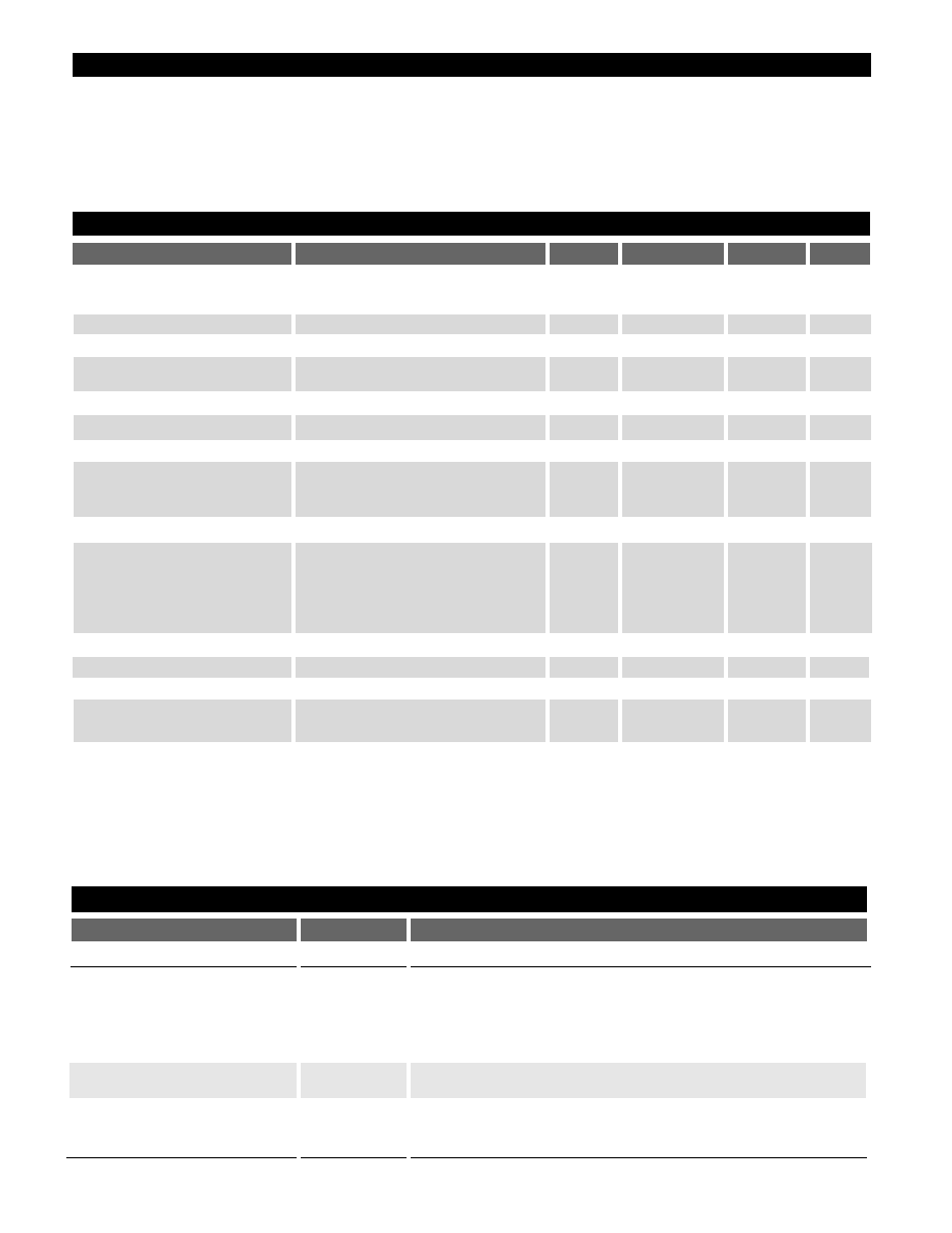
Typical Performance Characteristics
0
10
20
30
40
50
60
70
80
90
100 110 120 130
-0.150
-0.125
-0.100
-0.075
-0.050
-0.025
-0.000
0.025
0.050
0.075
0.100
T
J
(
∞
C)
Output V
oltage Deviation (%)
I
O
=10mA
V
IN
=2.75V
Output V
oltage Deviation (%)
Output Current (A)
T
Case
=0
∞C
T
Case
=25∞C
T
Case
=125
∞C
0.00
8.00
0.000
0.200
0.225
0.250
0.175
0.150
0.125
0.100
0.075
0.050
0.025
1.00
2.00
3.00
4.00
5.00
6.00
7.00
0
10
20
30
40
50
60
70
80 90
100 110 120 130
60.00
65.00
70.00
75.00
80.00
85.00
90.00
T
Case
(
∞
C)
Adjust Pin Current (
m
A)
I
O
=10mA
Reference Voltage vs. Temperature
Load Regulation vs. Output Current
Adjust Pin Current vs Temperature
72.4
72.2
72.0
71.8
71.6
71.4
71.2
71.0
70.8
70.6
70.4
0.0
0.8
1.6
3.2
4.0
5.6
6.4
7.2
I
OUT
(A)
Adjust Pin Current (
m
A)
70.2
70.0
72.6
2.4
4.8
8.0
Adjust Pin Current vs. I
OUT
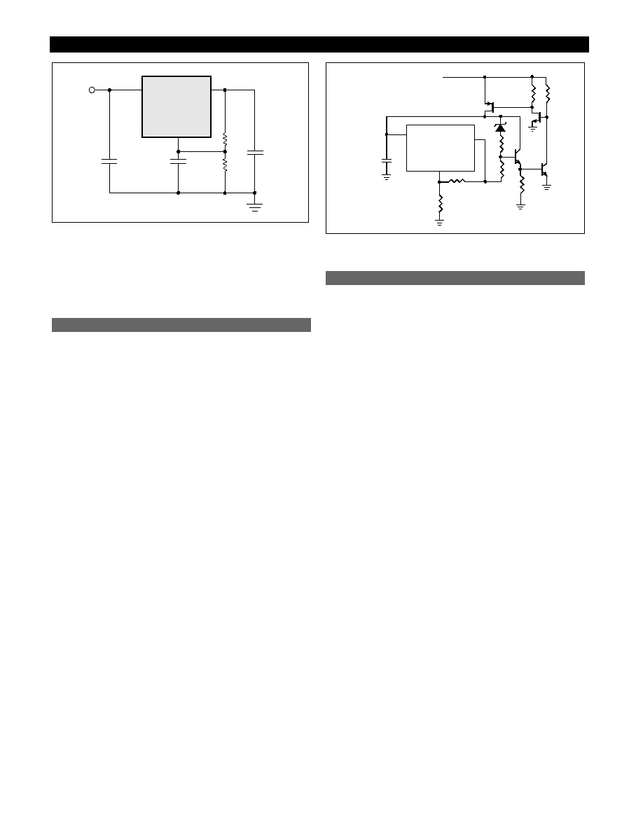
Application Notes
The CS5208-1 linear regulator has a composite PNP-NPN
output stage that requires an output capacitor for stability.
A detailed procedure for selecting this capacitor is includ-
ed in the Stability Considerations section.
Design Guidelines
This LDO adjustable regulator has an output voltage range
of 1.25V to 4.5V. An external resistor divider sets the out-
put voltage as shown in Figure 1. The regulator’s voltage
sensing error amplifier maintains a fixed 1.25V reference
between the output pin and the adjust pin.
A resistor divider network R
1
and R
2
causes a fixed current
to flow to ground. This current creates a voltage across R2
that adds to the 1.25V across R
1
and sets the overall output
voltage. The adjust pin current (typically 50µA) also flows
through R
2
and adds a small error that should be taken
into account if precise adjustment of Vout is necessary. The
output voltage is set according to the formula:
V
OUT
= V
REF
¥
+ R
2
¥ I
Adj
The term I
Adj
¥ R
2
represents the error added by the adjust
pin current.
R
1
is chosen so that the minimum load current is a least
10mA. R
1
and R
2
should be of the same composition for
best tracking over temperature. The divider resistors
should be placed as close to the IC as possible and connect-
ed to the output with a separate metal trace.
R
1
+ R
2
R
1
Adjustable Operation
Theory of Operation
CS5208-1
4
20.0
18.0
16.0
14.0
12.0
10.0
8.0
6.0
4.0
2.0
0.0
0.0
0.5
1.0
1.5
2.0
2.5
3.0
3.5
Output Current (A)
V
IN
-V
OUT
(V)
4.0
4.5
5.0
5.5
Dropout V
oltage (V)
Output Current (A)
0.00
0.25
0.50
0.75
1.00
1.25
0.0
7.0
6.0
5.0
4.0
3.0
2.0
1.0
8.0
1.00
2.00
3.00
4.00
5.00
Minimum Load Current (mA)
V
IN
≠ V
OUT
(V)
0.80
0.82
0.88
0.90
0.98
1.00
T
CASE
= 23
∞C
0.84
0.86
0.92
0.94
0.96
T
CASE
= 125
∞C
T
CASE
= 0
∞C
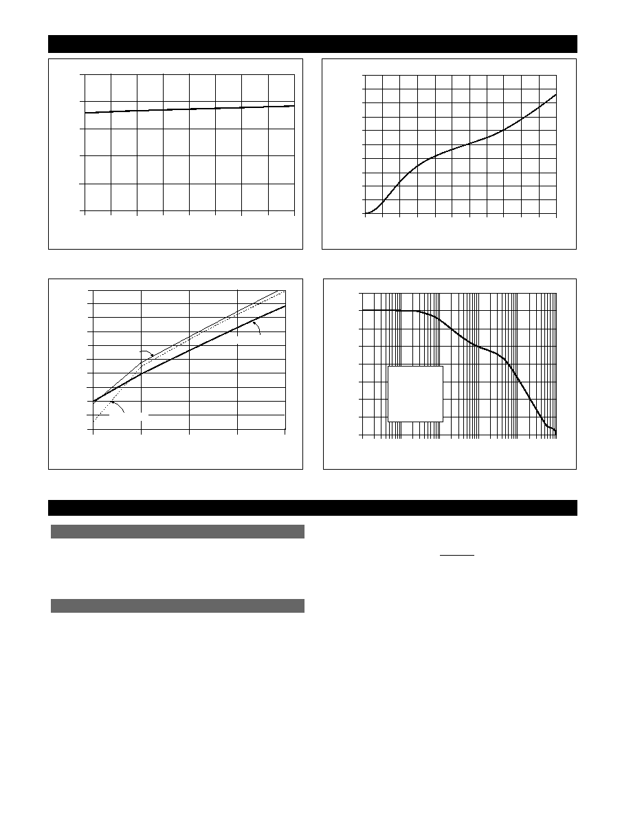
Typical Performance Characteristics: continued
Dropout Voltage vs. Output Current
Short Circuit Current vs. V
IN
- V
OUT
Minimum Load Current vs. V
IN
- V
OUT
10
1
10
2
10
3
10
4
10
5
20.0
30.0
50.0
70.0
90.0
Frequency (Hz)
Ripple Rejection (dB)
80.0
60.0
40.0
10.0
V
IN
- V
OUT
= 2V
V
Ripple
= 1V
PP
I
OUT
= 4A
C
Adj
= 0.1
mF
C
OUT
= 22
mF
10
6
Ripple Rejection vs. Frequency
CS5208-1
Application Notes: continued
5
Figure 1.
While not required, a bypass capacitor connected between
the adjust pin and ground will improve transient response
and ripple rejection. A 0.1µF tantalum capacitor is recom-
mended for “first cut” design. Value and type may be var-
ied to optimize performance vs price.
The CS5208-1 linear regulator has an absolute maximum
specification of 6V for the voltage difference between V
IN
and V
OUT
. However, the IC may be used to regulate volt-
ages in excess of 6V. The main considerations in such a
design are power-up and short circuit capability.
In most applications, ramp-up of the power supply to V
IN
is fairly slow, typically on the order of several tens of mil-
liseconds, while the regulator responds in less than one
microsecond. In this case, the linear regulator begins charg-
ing the output capacitor as soon as the V
IN
to V
OUT
differ-
ential is large enough that the pass transistor conducts cur-
rent. V
OUT
is essentially at ground, and V
IN
is on the order
of several hundred millivolts, so the pass transistor is in
dropout. As V
IN
increases, the pass transistor will remain
in dropout, and current is passed to the load until V
OUT
is
in regulation. Further increase in V
IN
brings the pass tran-
sistor out of dropout. The result is that the output voltage
follows the power supply ramp-up, staying in dropout
until the regulation point is reached. In this manner, any
output voltage may be regulated. There is no theoretical
limit to the regulated voltage as long as the V
IN
to V
OUT
differential of 6V is not exceeded.
However, the maximum ratings of the IC will be exceeded
in a short circuit condition. Short circuit conditions will
result in the immediate operation of the pass transistor
outside of its safe operating area. Over-voltage stresses will
then cause destruction of the pass transistor before over-
current or thermal shutdown circuitry can become active.
Additional circuitry may be required to clamp V
IN
to V
OUT
differential to less than 6V if failsafe operation is required.
One possible clamp circuit is illustrated below; however,
the design of clamp circuitry must be done on an applica-
tion by application basis. Care must be taken to ensure the
clamp actually protects the design. Components used in
the clamp design must be able to withstand the short cir-
cuit conditions indefinitely while protecting the IC.
Figure 2.
The output compensation capacitor helps determine three
main characteristics of a linear regulator: start-up delay,
load transient response, and loop stability.
The capacitor value and type is based on cost, availability,
size and temperature constraints. A tantalum or aluminum
electrolytic capacitor is best, since a film or ceramic capaci-
tor with almost zero ESR can cause instability. The alu-
minum electrolytic capacitor is the least expensive solu-
tion. However, when the circuit operates at low tempera-
tures, both the value and ESR of the capacitor will vary
considerably. The capacitor manufacturer’s data sheet pro-
vides this information.
A 300µF tantalum capacitor will work for most applica-
tions, but with high current regulators such as the
CS5208-1 the transient response and stability improve with
higher values of capacitance. The majority of applications
for this regulator involve large changes in load
current so the output capacitor must supply the instanta-
neous load current. The ESR of the output capacitor causes
an immediate drop in output voltage given by:
∆V = ∆I
¥ ESR.
For microprocessor applications it is customary to use an
output capacitor network consisting of several tantalum
and ceramic capacitors in parallel. This reduces the overall
ESR and reduces the instantaneous output voltage drop
under transient load conditions. The output capacitor net-
work should be as close to the load as possible for the best
results.
Protection Diodes
When large external capacitors are used with a linear regu-
lator it is sometimes necessary to add protection diodes. If
the input voltage of the regulator gets shorted, the output
capacitor will discharge into the output of the regulator.
The discharge current depends on the value of the capaci-
tor, the output voltage, and the rate at which V
IN
drops. In
the CS5208-1 regulator, the discharge path is through a
large junction and protection diodes are not usually need-
ed. If the regulator is used with large values of output
capacitance and the input voltage is instantaneously short-
Stability Considerations
V
IN
V
OUT
V
Adj
EXTERNAL SUPPLY
Other Adjustable Operation Considerations
V
OUT
V
IN
CS5208-1
R1
Adj
R2