Features
CS5231-3
500mA, 3.3V Linear Regulator
with Auxiliary Control
CS5231-3
Description
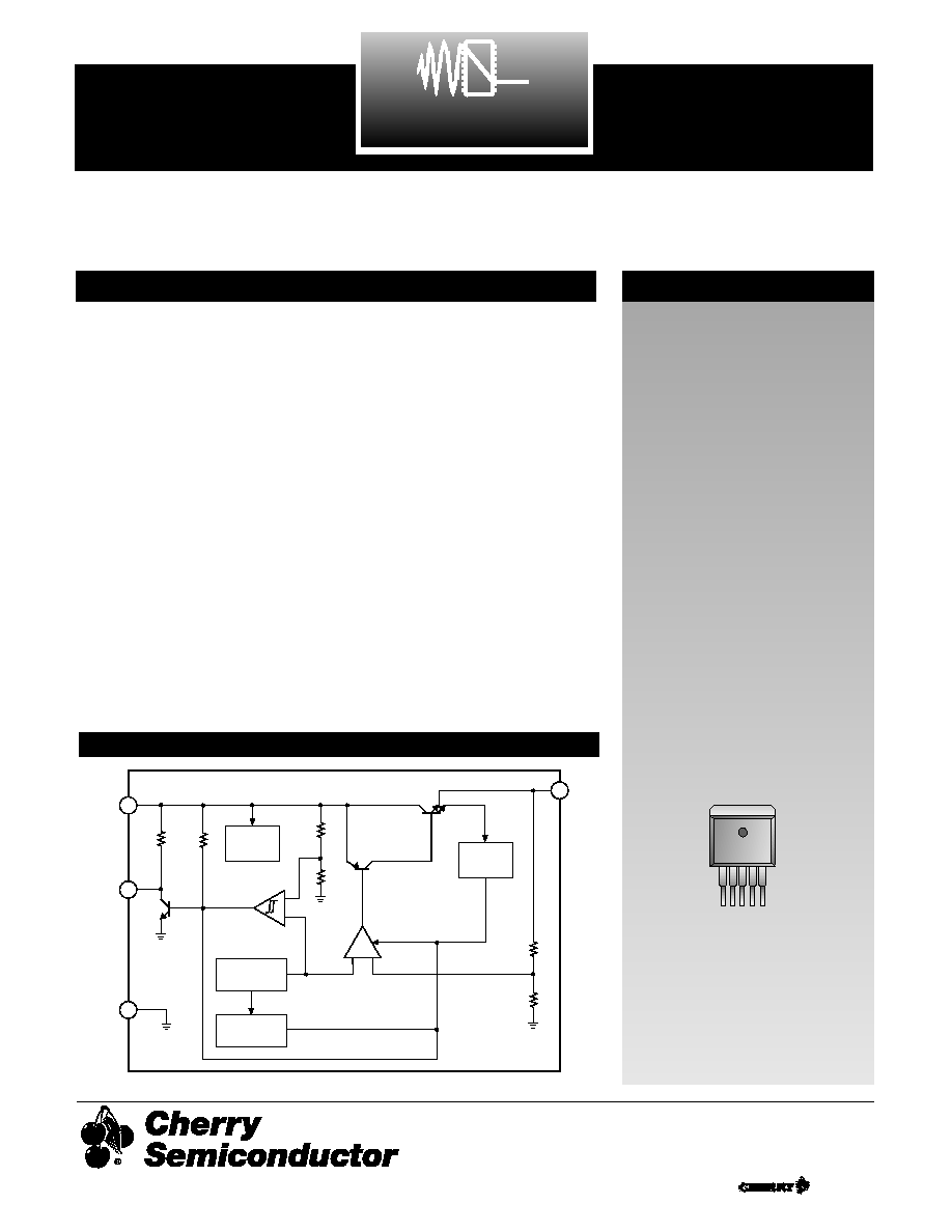
Block Diagram
1
1
1. No Connect
2. V
IN
3. Gnd
4. V
OUT
5. AuxDrv
Tab = Gnd
A Company
Æ
Rev. 3/31/99
Cherry Semiconductor Corporation
2000 South County Trail, East Greenwich, RI 02818
Tel: (401)885-3600 Fax: (401)885-5786
Email: info@cherry-semi.com
Web Site: www.cherry-semi.com
Consult factory for other package
options.
The CS5231-3 combines a three-
terminal linear regulator with cir-
cuitry to control an external PFET
transistor with the intent of manag-
ing two input supplies. A 5V sup-
ply powers the regulator while an
auxiliary 3.3V supply is controlled
by the IC. The design has been opti-
mized to provide a "glitch-free"
transition between the two sup-
plies.
The CS5231-3 linear regulator pro-
vides a fixed 3.3V output @ 500mA
with an overall accuracy of ± 2%.
The NPN-PNP composite pass tran-
sistor provides a low dropout volt-
age and requires less supply cur-
rent than PNP designs. Full protec-
tion including current limit and
thermal shutdown is provided.
Also designed for low reverse cur-
rent, the IC prevents excessive cur-
rent from flowing from the output
to ground if the regulator input
voltage is lower than the output
voltage.
The CS5231-3 also controls an auxil-
iary supply that can provide power
to the regulator output when input
voltage for the regulator is not
available. The AuxDrv auxiliary
output is normally pulled up to the
regulator input voltage and drives
low whenever the input voltage
drops below 4.4V (nominal). It is
typically used to control a PFET
switch that connects a 3.3V auxil-
iary supply to the regulator output.
The CS5231-3 is available in a
5-lead D
2
PAK (TO-263) package.
Applications include Network
Interface Cards (NICs), modem
cards and power supplies with
multiple input sources.
Linear Regulator
s
3.3V ± 2% Output Voltage
s
3mA Quiescent Current
@ 500mA
s
Fast Transient Response
s
Current Limit
s
Thermal Shutdown with
Hysteresis
s
450µA Reverse Output
Current
s
Fast Transient Response
System Power Management
s
Auxiliary Supply Control
-
+
-
+
Internal
Bias
Bandgap
Reference
Thermal
Shutdown
Current
Limit
V
IN
10k
50k
AuxDrv
Gnd
V
IN
UV
Comparator
V
REF
Error
Amp
Shutdown
V
OUT
Package Options
5 Lead D
2
PAK
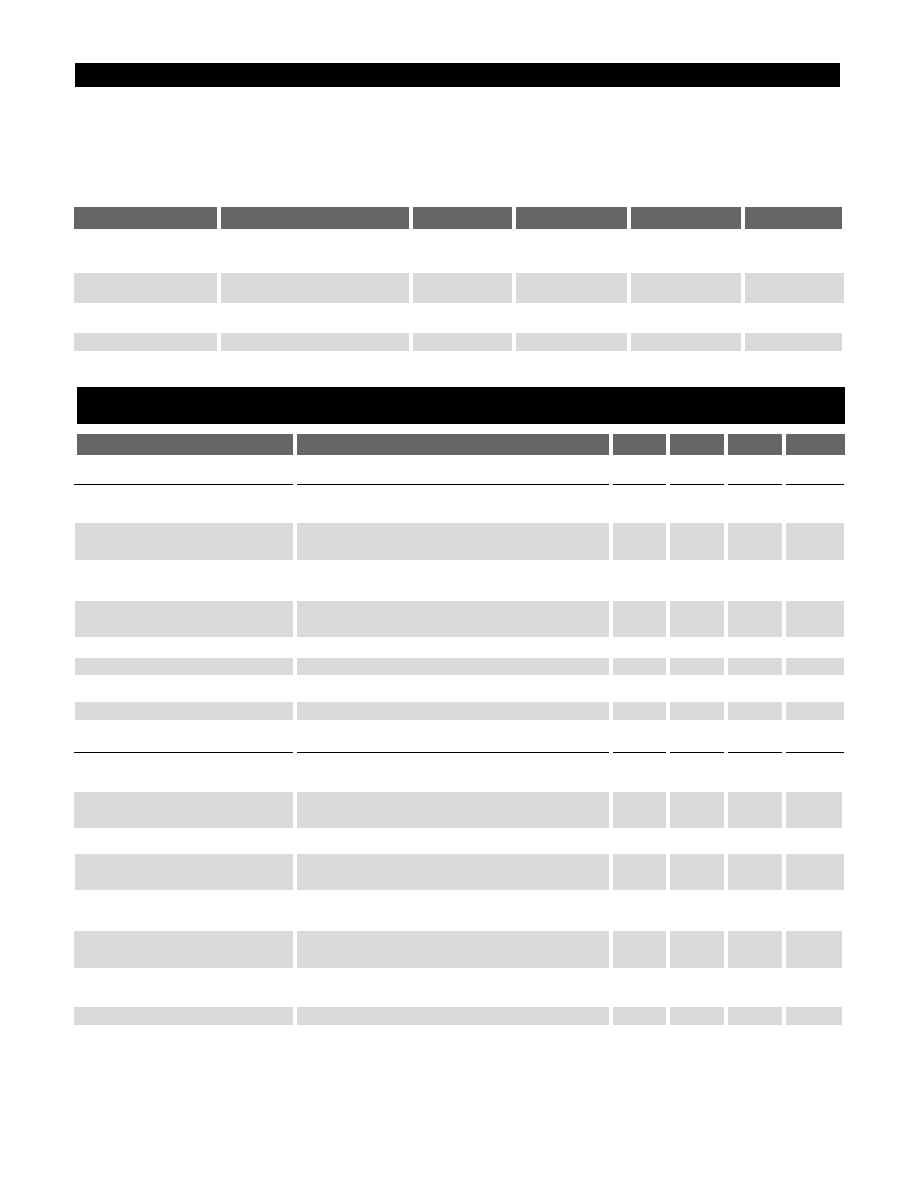
Electrical Characteristics:
0∞C < T
A
< 70∞C, 0∞C < T
J
< 125∞C, 4.75V V
CC
< 6V, C
OUT
10µF with ESR < 1,
I
OUT
= 10mA, unless otherwise specified.
PARAMETER
TEST CONDITIONS
MIN
TYP
MAX
UNIT
CS5231-3
2
Absolute Maximum Ratings
Maximum Operating Junction Temperature ..........................................................................................................................150∞C
Storage Temperature Range .....................................................................................................................................-65∞C to +150∞C
Lead Temperature Soldering
Reflow (SMD styles only) ...........................................................................................60 sec. max above 183∞C, 230∞C peak
ESD Damage Threshold (Human Body Model)....................................................................................................................2kV
PIN SYMBOL
PIN NAME
V
MAX
V
MIN
I
SOURCE
I
SINK
V
IN
IC Power Input
14V
-0.3V
100mA
Internally
Limited
V
OUT
Output Voltage
6V
-0.3V
Internally
100mA
Limited
AuxDrv
Auxiliary Drive Output
14V
-0.3V
10mA
50mA
Gnd
IC Ground
N/A
N/A
N/A
N/A
s
Linear Regulator
Output Voltage
10mA < I
OUT
< 500mA
3.234
3.300
3.366
V
-2%
+2%
Line Regulation
I
OUT
= 10mA,
1
5
mV
V
IN
= 4.75V to 6V
Load Regulation
V
IN
= 5V,
5
15
mV
I
OUT
= 10mA to 500mA
Ground Current
I
OUT
= 10mA
2
3
mA
I
OUT
= 500mA
3
6
mA
Reverse Current
V
IN
= 0V, V
OUT
= 3.3V
0.45
1
mA
Current Limit
0V < V
OUT
< 3.2V
0.55
0.85
1.2
A
Thermal Shutdown
Note 1
150
180
210
∞C
Thermal Shutdown Hysteresis
Note 1
25
∞C
s
Auxiliary Drive
Upper V
IN
Threshold
Increase V
IN
until regulator turns on
4.35
4.5
4.65
V
and AuxDrv drives high
Lower V
IN
Threshold
Decrease V
IN
until regulator turns off
4.25
4.4
4.55
V
and AuxDrv drives low
V
IN
Threshold Hysteresis
75
100
125
mV
Output Low Voltage
I
AuxDrv
= 100µA,
0.1
0.4
V
1V < V
IN
< 4.5V
Output Low Peak Voltage
Increase V
IN
from 0V to 1V.
0.65
0.9
V
Record peak AuxDrv output voltage
AuxDrv Current Limit
V
AuxDrv
= 1V,
0.5
6
25
mA
V
IN
= 4.0V
Response Time
Step V
IN
from 5V to 4V, measure time
1
10
µs
for V
AuxDrv
to drive low. Note 1
Pull-Up/Down Resistance
V
IN
= 0V and V
IN
> 4.7V
5
10
25
k
Note 1: Guaranteed by design, not 100% production tested. Thermal shutdown is 100% functionally tested at wafer
probe.

CS5231-3
Package Pin Description
PACKAGE PIN #
PIN SYMBOL
FUNCTION
3
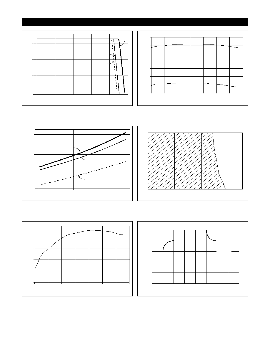
Typical Performance Characteristics
Output Voltage vs. Junction Temperature
Load Regulation (mV)
I
OUT
(A)
1.2
1.0
0.8
0.6
0.4
0.2
0.0
0.0
0.2
0.4
125∞C
27∞C
0∞C
Load Regulation vs. I
OUT
Over Temperature
Line Regulation vs. I
OUT
Over Temperature
Reverse Current (
µ
A)
390
380
370
360
0
20
40
60
80
100
120
Junction Temperature (∞C)
Reverse Current vs. Junction Temperature
5Lead D
2
PAK
1
N/C
No connection.
2
V
IN
Input voltage.
3
Gnd
Ground and IC substrate connection (case).
4
V
OUT
Regulated output voltage.
5
AuxDrv
Output used to control an auxiliary supply voltage. This lead is
driven low if V
IN
is less than 4.5V, and is otherwise pulled up
to V
IN
through an internal 10k resistor.
Output V
oltage (V)
3.302
3.300
3.298
3.296
0
20
40
60
80
100
120
Junction Temperature (∞C)
I
OUT
= 10mA
I
OUT
= 500mA
Line Regulation (
µ
V)
I
OUT
(A)
80
70
60
50
40
0.0
0.2
0.4
27∞C
0∞C
125∞C
4.75V <V
IN
< 6V
CS5231-3
4
Typical Performance Characteristics: continued
Ground Current (mA)
Load Current (A)
2.6
2.4
2.2
2.0
1.8
1.6
0.0
0.2
0.4
T
J
= 0∞C
I
Gnd
@ 0∞C
T
J
= 27∞C
I
Gnd
@ 27∞C
T
J
= 125∞C
I
Gnd
@ 125∞C
Ground Current vs. Load Current
Temperature (C)
Current Limit (mA)
5.000
4.800
4.600
4.400
4.200
4.000
0
20
40
60
80
100
120
140
AuxDrv Current Limit vs. Junction Temperature
V
OUT
(V)
I
OUT
(A)
3
2
1
0
0.0
0.2
0.4
125∞C
27∞C
0∞C
0.6
0.8
1.0
V
OUT
vs. I
OUT
Over Temperature
V
IN
Threshold V
oltage (V)
Junction Temperature (C)
4.520
4.500
4.480
4.460
4.440
4.420
4.400
4.380
0
20
40
60
80
100
120
140
V
IN
Turn-on
Threshold
V
IN
Turn-on
Threshold
V
IN
Thresholds vs. Junction Temperature
6.0
5.0
4.0
3.0
2.0
1.0
0.0
10
100
1000
7.0
Capacitance (
µ
F)
Capacitance ESR()
Region of Stable Operation
3.400
3.300
3.200
500mA
10mA
Time, 5µs per division
V
OUT
I
OUT
C
IN
= 33µF
C
OUT
= 33µF
V
IN
= 5.00V
Transient Response

Theory of Operation
The CS5231-3 is a fixed 3.3V linear regulator that contains
an auxiliary drive control feature. When V
IN
is greater than
the typical 4.5V threshold, the IC functions as a linear regu-
lator. It provides up to 500mA of current to a load through
a composite PNP-NPN pass transistor. An output capacitor
greater than 10µF with equivalent series resistance less
than 1 is required for compensation. More information is
provided in the Stability Considerations section.
The CS5231-3 provides an auxiliary drive feature that
allows a load to remain powered even if the V
IN
supply for
the IC is absent. An external p-channel FET is the only
additional component required to implement this function
if an auxiliary power supply is available. The PFET gate is
connected to the AuxDrv lead. The PFET drain is connect-
ed to the auxiliary power supply, and the PFET source is
connected to the load. The polarity of this connection is
very important, since the PFET body diode will be connect-
ed between the load and the auxiliary supply. If the PFET
is connected with its drain to the load and its source to the
supply, the body diode will be forward-biased if the auxil-
iary supply is turned off. This will result in the linear regu-
lator providing current to everything on the auxiliary sup-
ply rail.
The AuxDrv lead is internally connected to a 10k resistor
and to a saturating NPN transistor that acts as a switch. If
the V
IN
supply is off, the AuxDrv output will connect the
PFET gate to ground through the 10k resistor, and the
PFET will conduct current to the load.
As the V
IN
supply begins to rise, the AuxDrv lead will also
rise until it reaches a typical voltage of about 650mV. The
NPN transistor connected to the AuxDrv lead will saturate
at this point, and the gate of the PFET will be pulled down
to a typical voltage of about 100mV. The PFET will contin-
ues to conduct current to the load.
The V
IN
supply voltage will continue to rise, but the linear
regulator output is disabled until V
IN
reaches a typical
threshold of 4.5V. During this time, the load continues to
be powered by the auxiliary driver. Once the 4.5V V
IN
threshold is reached, the saturating NPN connected to the
AuxDrv lead turns off. The on-chip 10k pull-up resistor
will pull the PFET gate up to V
IN
, thus turning the PFET
off. The linear regulator turns on at the same time. An
external compensation capacitor is required for the linear
regulator to be stable, and this capacitance also serves as a
charge reservoir to minimize any "glitching" that might
result during the supply changeover. Hysteresis is present
in the AuxDrv circuitry, requiring V
IN
to drop by 100mV
(typical) after the linear regulator is providing power to the
load before the AuxDrv circuitry can be re-enabled.
CS5231-3
5
Application Information
V
IN
V
OUT
V
AUXDRV
I
OUT
= STARTUP 375mA
Figure 1. Initial power-up, V
AUX
not present R
OUT
= 8.8.
Application Circuit
+5V PCI
C1
33µF
V
IN
Gnd
V
OUT
AuxDrv
CS5231-3
M1
+3.3V V
AUX
C1
33µF
C3
33µF
ASIC
V
DD
*indicates PFET body diode
V
IN
V
OUT
V
AUXDRV
I
OUT
= 375mA V
AUX
= 3.30V
Figure 2a. Power-up, V
AUX
= 3.30V. Note the "oscillatory performance"
as the linear regulator charges the V
OUT
node. I
OUT
◊ R
DS(ON)
130mV

CS5231-3
6
Stability Considerations
The output capacitor helps determine three main charac-
teristics of a linear regulator: startup, transient response
and stability.
Startup is affected because the output capacitor must be
charged. At initial startup, the V
IN
supply may not be pre-
sent, and the output capacitor will be charged through the
PFET. The PFET will initially provide current to the load
through its body diode. The diode will act as a voltage fol-
lower until sufficient voltage is present to turn the FET on.
Since most commercial power supplies have a fairly low
ramp rate, charging through the body diode should effec-
tively limit in-rush current to the capacitor.
During normal operation, transient load current require-
ments will be satisfied from the charge stored in the output
capacitor until either the linear regulator or the auxiliary
supply can respond. Larger values of capacitance will
improve transient response, but will also cost more. A lin-
ear regulator will respond within microseconds, where an
external power supply may take milliseconds to react. The
output capacitance will provide the difference in current
until this occurs. The result will be an instantaneous volt-
age change at the output. This change is the product of the
current change and the capacitor ESR:
Application Information: continued
V
IN
V
OUT
V
AUXDRV
I
OUT
= 375mA V
AUX
= 3.30
Figure 3b. Power-down, V
AUX
= 3.135V. The difference in voltage is
now I
OUT
◊ R
DS(ON)
plus the difference in supply voltages (3.30 -V
AUX
).
V
IN
V
OUT
V
AUXDRV
I
OUT
= 375mA V
AUX
= 3.465
V
IN
V
OUT
V
AUXDRV
I
OUT
= 375mA V
AUX
= 3.135V
V
IN
V
OUT
V
AUXDRV
I
OUT
= 375mA V
AUX
= 3.135
Figure 4a. Power-up, V
AUX
= 3.465V. I
OUT
◊ R
DS(ON)
is compensated by
the higher value of V
AUX
V
IN
V
OUT
V
AUXDRV
I
OUT
= 375mA V
AUX
= 3.465
Figure 2b. Power-down, V
AUX
= 3.30V. Again, note V = I
OUT
R
DS(ON)
130mV.
Figure 3a. Power-up, V
AUX
= 3.135V. The "oscillatory performance"
mode lasts longer because the difference between V
AUX
and 3.30 is
greater.
Figure 4b. Power-down, V
AUX
= 3.465V.

V
OUT
= (I
LOAD
) (ESR)
This limitation directly affects load regulation. Capacitor
ESR must be minimized if output voltage must be main-
tained within tight tolerances. In such a case, it is often
advisable to use a parallel network of different types of
capacitors. For example, electrolytic capacitors provide
high charge storage capacity in a small size, while tantalum
capacitors have low ESR. The parallel combination will
result in a high capacity, low ESR network. It is also impor-
tant to physically locate the capacitance network close to
the load, and to connect the network to the load with wide
PC board traces to minimize the metal resistance.
The CS5231-3 has been carefully designed to be stable for
output capacitances greater than 10µF with equivalent
series resistance less than 1. While careful board layout is
important, the user should have a stable system if these
constraints are met. A graph showing the region of stability
for the CS5231-3 is included in the "Typical Performance
Characteristics" section of this data sheet.
Input Capacitors and the V
IN
Thresholds
A capacitor placed on the V
IN
pin will help to improve
transient response. During a load transient, the input
capacitor serves as a charge "reservoir", providing the
needed extra current until the external power supply can
respond. One of the consequences of providing this current
is an instantaneous voltage drop at V
IN
due to capacitor
ESR. The magnitude of the voltage change is again the
product of the current change and the capacitor ESR.
It is very important to consider the maximum current step
that can exist in the system. If the change in current is large
enough, it is possible that the instantaneous voltage drop
on V
IN
will exceed the V
IN
threshold hysteresis, and the IC
will enter a mode of operation resembling an oscillation.
As the part turns on, the output current I
OUT
will increase,
reaching current limit during initial charging. Increasing
I
OUT
results in a drop at V
IN
such that the shutdown
threshold is reached. The part will turn off, and the load
current will decrease. As I
OUT
decreases, V
IN
will rise and
the part will turn on, starting the cycle all over again. This
oscillatory operation is most likely at initial startup when
the output capacitance is not charged, and in cases where
the ramp-up of the V
IN
supply is slow. It may also occur
during the power transition when the linear regulator
turns on and the PFET turns off. a 15µs delay exists
between turn-on of the regulator and the AUXDRV pin
pulling the gate of the PFET high. This delay prevents
"chatter" during the power transitions. During this inter-
val, the linear regulator will attempt to regulate the output
voltage as 3.3V. If the output voltage is significantly below
3.3V, the IC will go into current limit while trying to raise
V
OUT
. It is a short-lived phenomenon and is mentioned
here to alert the user that the condition can exist. It is typi-
cally not a problem in applications. Careful choice of the
PFET switch with respect to R
DS(ON)
will minimize the volt-
age drop which the output must charge through to return
to a regulated state. More information is provided in the
section on choosing the PFET switch.
If required, using a few capacitors in parallel to increase
the bulk charge storage and reduce the ESR should give
better performance than using a single input capacitor.
Short, straight connections between the power supply and
V
IN
lead along with careful layout of the PC board ground
plane will reduce parasitic inductance effects. Wide V
IN
and V
OUT
traces will reduce resistive voltage drops.
Choosing the PFET Switch
The choice of the external PFET switch is based on two
main considerations. First, the PFET should have a very
low turn-on threshold. Choosing a switch transistor with
V
GS(ON)
1V ensures the PFET will be fully enhanced with
only 3.3V of gate drive voltage. Second, the switch transis-
tor should be chosen to have a low R
DS(ON)
to minimize the
voltage drop due to current flow in the switch. The formu-
la for calculating the maximum allowable on-resistance is
R
DS(ON)(MAX)
=
where V
AUX(MIN)
is the minimum value of the auxiliary
supply voltage, V
OUT(MIN)
is the minimum allowable out-
put voltage, I
OUT(MAX)
is the maximum output current and
1.5 is a "fudge factor" to account for increases in R
DS(ON)
due to temperature.
Output Voltage Sensing
It is not possible to remotely sense the output voltage of
the CS5231-3 since the feedback path to the error amplifier
is not externally available. It is important to minimize volt-
age drops due to metal resistance of high current PC board
traces. Such voltage drops can occur in both the supply
traces and the return traces.
The following board layout practices will help to minimize
output voltage errors:
∑ Always place the linear regulator as close to both load
and output capacitors as possible.
∑ Always use the widest possible traces to connect the lin-
ear regulator to the capacitor network and to the load.
∑ Connect the load to ground through the widest possible
traces.
∑ Connect the IC ground to the load ground trace at the
point where it connects to the load.
Current Limit
The CS5231-3 has internal current limit protection. Output
current is limited to a typical value of 850mA, even under
output short circuit conditions. If the load current drain
exceeds the current limit value, the output voltage will be
pulled down and will result in an out of regulation condi-
tion. The IC does not contain circuitry to report this fault.
Thermal Shutdown
The CS5231-3 has internal temperature monitoring circuit-
ry. The output is disabled if junction temperature of the IC
reaches a typical value of 180∞C. Thermal hysteresis is typi-
V
AUX(MIN)
- V
OUT(MIN)
1.5 ◊ I
OUT(MAX)
CS5231-3
7
Application Information: continued
cally 25∞C and allows the IC to recover from a thermal
fault without the need for an external reset signal. The
monitoring circuitry is located near the composite PNP-
NPN output transistor, since this transistor is responsible
for most of the on-chip power dissipation. The combina-
tion of current limit and thermal shutdown will protect the
IC from nearly any fault condition.
Reverse Current Protection
During normal system operation, the auxiliary drive cir-
cuitry will maintain voltage on the V
OUT
pin when V
IN
is
absent. IC reliability and system efficiency are improved
by limiting the amount of reverse current that flows from
V
OUT
to ground and from V
OUT
to V
IN
. Current flows from
V
OUT
to ground through the feedback resistor divider that
sets up the output voltage. This resistor can range in value
from 6k to about 10k, and roughly 500µA will flow in
the typical case. Current flow from V
OUT
to V
IN
will be
limited to leakage current after the IC shuts down. On-chip
RC time constants are such that the output transistor
should be turned off well before V
IN
drops below the V
OUT
voltage.
Calculating Power Dissipation and
Heatsink Requirements
Most linear regulators operate under conditions that result
in high on-chip power dissipation. This results in high
junction temperatures. Since the IC has a thermal shut-
down feature, ensuring the regulator will operate correctly
under normal conditions is an important design considera-
tion. Some heatsinking will usually be required.
Thermal characteristics of an IC depend on four parame-
ters: ambient temperature (T
A
in ∞C), power dissipation
(P
D
in watts), thermal resistance from the die to the ambi-
ent air (
JA
in ∞C per watt) and junction temperature (T
J
in
∞C). The maximum junction temperature is calculated from
the formula below:
T
J(MAX)
= T
A(MAX)
+ (
JA
) (P
D(MAX)
)
Maximum ambient temperature and power dissipation are
determined by the design, while
JA
is dependent on the
package manufacturer. The maximum junction tempera-
ture for operation of the CS5231-3 within specification is
150∞C. The maximum power dissipation of a linear regula-
tor is given as
P
D(MAX)
= (V
in(MAX)
- V
OUT(MIN)
) (I
LOAD(MAX)
)
+ (V
IN (MAX)
) (I
Gnd(MAX)
)
where I
Gnd(MAX)
is the IC bias current.
It is possible to change the effective value of
JA
by adding
a heatsink to the design. A heatsink serves in some manner
to raise the effective area of the package, thus improving
the flow of heat from the package into the surrounding air.
Each material in the path of heat flow has its own charac-
teristic thermal resistance, all measured in ∞C per watt. The
thermal resistances are summed to determine the total
thermal resistance between the die junction and air. There
are three components of interest: junction-to-case thermal
resistance (
JC
), case-to-heatsink thermal resistance (
CS
)
and heatsink-to-air thermal resistance (
SA
). The resulting
equation for junction-to-air thermal resistance is
JA
=
JC
+
CS
+
SA
The value of
JC
for the CS5231-3 is provided in the
Packaging Information section of this data sheet.
CS
can
be considered zero, since heat is conducted out of the
package by the IC leads and the tab of the D
2
PAK package,
and since the IC leads and tab are soldered directly to the
PC board.
Modification of
SA
is the primary means of thermal man-
agement. For surface mount components, this means mod-
ifying the amount of trace metal that connects to the IC.
The thermal capacity of PC board traces is dependent on
how much copper area is used, whether or not the IC is in
direct contact with the metal, whether or not the metal sur-
face is coated with some type of sealant, and whether or
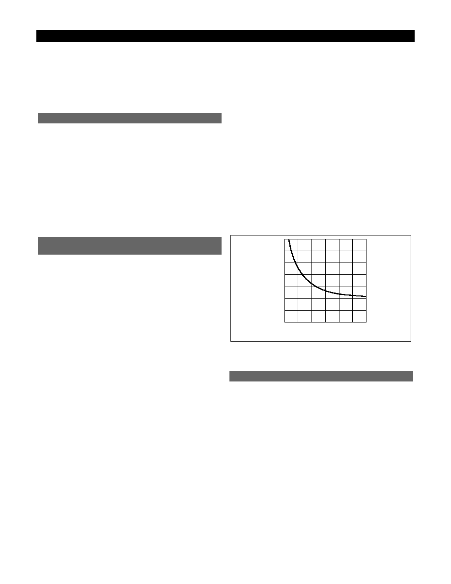
not there is airflow across the PC board. The chart provid-
ed below shows heatsinking capability of a square, single
sided copper PC board trace. The area is given in square
millimeters. It is assumed there is no airflow across the PC
board.
Figure 5: Thermal Resistance Capability of Copper PC Board Metal
Traces
Typical D
2
PAK PC Board Heatsink Design
A typical design of the PC board surface area needed for
the D
2
PAK package is shown below. Calculations were
made assuming V
IN(MAX)
=5.25V, V
OUT(MIN)
= 3.266V,
I
OUT(MAX)
= 500mA, I
Gnd(MAX)
= 5mA and T
A
= 70∞C.
P
D
= (5.25V - 3.266V) (0.5A) + (5.25V) (0.005A) = 1018mW
Maximum temperature rise T = T
J(MAX)
- T
A
=
150∞C - 70∞C = 80∞C.
JA
(worst case) = T/P
D
= 80∞C/1.018W = 78.56∞C/W
First, we determine the need for heatsinking. If we assume
the maximum
JA
= 50∞C/W for the D
2
PAK, the maximum
temperature rise is found to be
T = (P
D
) (
JA
) = (1.018W) (50∞C/W) = 50.9∞C
This is less than the maximum specified operating junction
temperature of 125∞C, and no heatsinking is required.
Since the D
2
PAK has a large tab, mounting this part to the
70
60
50
40
30
20
10
0
0
2000
4000
6000
Thermal Resistance,
∞
C/W
PC Board Trace Area (mm
2
)
8
CS5231-3
Application Information: continued

PC board by soldering both tab and leads will provide
superior performance with no PC board area penalty.
Description
The CS5231-3 application circuit has been implemented as
shown in the following pages. The schematic, bill of mate-
rials and printed circuit board artwork can be used to build
the circuit. The design is very simple and consists of two
capacitors, a p-channel FET and the CS5231-3. Five turret
pins are provided for connection of supplies, meters, oscil-
loscope probes and loads. The CS5231-3 power supply
management solution is implemented in an area less than
1.5 square inches. Due to the simplicity of the design, out-
put current must be derated if the CS5231-3 is operated at
V
IN
voltages greater than 7V. Figure 15 provides the derat-
ing curve on a maximum power dissipation if heatsink is
added. Operating at higher power dissipation without
heatsink may result in a thermal shutdown condition.
Figure 6: Demo Board Output Current Derating vs V
IN
The V
IN
Connection
The V
IN
connection is denoted as such on the PC board.
The maximum input voltage to the IC is 14V before dam-
age to the IC is possible. However, the specification range
for the IC is 4.75V < V
IN
< 6V.
The Gnd Connection
The Gnd connection ties the IC power return to two turret
pins. The extra turret pin provides for connection of multi-
ple instrument grounds to the demonstration board.
The AuxDrv Connection
The AuxDrv lead of the CS5231-3 is connected to the gate
of the external PFET. This connection is also brought to a
turret pin to allow easy connection of an oscilloscope probe
for viewing the AuxDrv waveforms.
The V
AUX
Connection
The V
AUX
turret pin provides a connection point between
an external 3.3V supply and the PFET drain.
The V
OUT
Connection
The V
OUT
connection is tied to the V
OUT
lead of the
CS5231-3 and the PFET source. This point provides a con-
venient point at which some type of lead may be applied.
Application Circuit Schematic
PC Board Layout Artwork
The PC board is a single layer copper design. The layout
artwork is reproduced at actual size below.
Top Copper Layer
Top Silk Screen Layer
AUX.DRV
AUX3.3V
V
OUT
3.3V
GND
GND
V
IN
5V
2"
1.5"
2"
1.5"
C1
V
IN
TP1
GND
TP2
TP3
TP5
TP6
AUXDRV
C2
V
IN
GND
AUXDRV
V
OUT
CS5231-3
Q1
TP4
+3.3V V
AUX
U1
600
500
400
300
200
100
0
5
6
7
8
9
10
11
12
13
14
V
IN
(VOLTS)
I
OUT
(mA)
Application Circuit Characteristics
CS5231-3
9

Application Circuit Bill of Materials
Application Circuit Characteristics: continued
Refdes
Description
Part Number
Manufacturer
Contact Information
C1, C2
33µF, 16V tantalum capacitors
TAJ336K016
AVX Corp
www.avxcorp.com
1-843-448-9411
Q1
p-channel FET transistor
MGSF1P02ELT1
Motorola
www.mot-sps.com
U1
Linear regulator with auxiliary
CS5231-3DPS
Cherry Semiconductor
www.cherry-sem.com
1-800-272-3601
T1-T6
Turret pins
40F6023
Newark Electronics
www.newark.com
1-800-463-9275
10
Test Descriptions
The startup and supply transition waveforms shown in fig-
ures 1 through 4b were obtained using the application cir-
cuit board with a resistive load of 8.8. This provides a DC
load of 375mA when the regulated output voltage is 3.3V.
A standard 2A bench supply was used to provide power to
the application circuit. The transient response waveforms
shown in the Typical Performance Characteristics section
were obtained by switching a 6.3 resistor across the out-
put.
Temperature Performance
The graph below shows thermal performance for the
CS5231-3 across the normal operating output current range.
Figure 7: Package Temperature vs Load Current (V
IN
= 5V, T
A
=23 C∞)
PFET R
DS(ON)
Performance
The graph provided below show typical R
DS(ON)
perfor-
mance for the PFET. The data is provided as V
DS
vs I
OUT
for different values of V
AUX
.
Figure 8: PFET Vds vs I
OUT
140
120
100
80
60
40
0
100
200
300
400
500
I
OUT
(mA)
Vds (mV)
160
20
0
V
AUX
= 3.465V
V
AUX
= 3.135V
V
AUX
= 3.300V
50
45
40
35
30
25
0
50
100
150
200
250
300
350
400
450
500
Load Current (mA)
Package T
emperature
(C)
20
55
CS5231-3

Cherry Semiconductor Corporation reserves the right to
make changes to the specifications without notice. Please
contact Cherry Semiconductor Corporation for the latest
available information.
PACKAGE DIMENSIONS IN mm (INCHES)
11
Rev. 3/31/99
Package Specification
PACKAGE THERMAL DATA
Ordering Information
Part Number
Description
CS5231-3GDP5
5 Lead D
2
PAK
CS5231-3GDPR5
5 Lead D
2
PAK (tape & reel)
© 1999 Cherry Semiconductor Corporation
CS5231-3
Thermal Data
5Lead
D
2
PAK
R
JC
typ
2.5
∞C/W
R
JA
typ
10-50*
∞C/W
*Depending on thermal properties of substrate. R
JA
= R
JC
+ R
CA
5 Lead D
2
PAK (DP)
1.70 (.067) REF
0.10 (.004)
0.00 (.000)
10.31 (.406)
10.05 (.396)
0.91 (.036)
0.66 (.026)
1.40 (.055)
1.14 (.045)
4.57 (.180)
4.31 (.170)
1.68 (.066)
1.40 (.055)
2.74(.108)
2.49(.098)
.254 (.010) REF
2.79 (.110)
2.29 (.090)
15.75 (.620)
14.73 (.580)
8.53 (.336)
8.28 (.326)