 | –≠–ª–µ–∫—Ç—Ä–æ–Ω–Ω—ã–π –∫–æ–º–ø–æ–Ω–µ–Ω—Ç: CS52510-1 | –°–∫–∞—á–∞—Ç—å:  PDF PDF  ZIP ZIP |
Features
s
1.25V to 5V V
OUT
at 10A
s
V
POWER
Dropout < 0.65V @
10A
s
V
CONTROL
Dropout < 1.25V @
10A
s
1.5% Trimmed Reference
s
Fast Transient Response
s
Remote Voltage Sensing
s
Thermal Shutdown
s
Current Limit
s
Short Circuit Protection
s
Backwards Compatible with
3-pin Regulators
Package Options
CS52510-1
10A LDO 5-Pin Adjustable Linear Regulator
CS52510-1
Description
5 Lead TO-220
1
1. V
SENSE
2. Adjust
3. V
OUT
4. V
CONTROL
5. V
POWER
Tab = V
OUT
1
A Company
®
Rev. 3/17/99
Cherry Semiconductor Corporation
2000 South County Trail, East Greenwich, RI 02818
Tel: (401)885-3600 Fax: (401)885-5786
Email: info@cherry-semi.com
Web Site: www.cherry-semi.com
This new very low dropout regula-
tor is designed to power the next
generation of advanced micropro-
cessor. To achieve very low
dropout, the internal pass transistor
is powered separately from the con-
trol circuitry. Furthermore, with the
control and power inputs tied
together, this device can be used in
single supply configuration and
still offer a better dropout voltage
than conventional PNP-NPN based
LDO regulators. In this mode the
dropout is determined by the mini-
mum control voltage.
It is supplied in a five-terminal
TO-220 package, which allows for
the implementation of a remote-
sense pin permitting very accurate
regulation of output voltage direct-
ly at the load, where it counts,
rather than at the regulator. This
remote sensing feature virtually
eliminates output voltage variations
due to load changes and resistive
voltage drops. Typical load regula-
tion measured at the sense pin is
1mV for an output voltage of 2.5V
with a load step of 10mA to 10A.
The very fast transient loop
response easily meets the needs of
the latest microprocessors. In addi-
tion, a small capacitor on the Adjust
pin will further improve the tran-
sient capabilities.
Internal protection circuitry pro-
vides for “bust-proof” operation,
similar to three-terminal regulators.
This circuitry, which includes over-
current, short circuit, supply
sequencing and overtemperature
protection, will self protect the reg-
ulator under all fault conditions.
The CS52510-1 is ideal for generat-
ing a secondary 2 - 2.5V low voltage
supply on a motherboard where
both 5V and 3.3V are already
available.
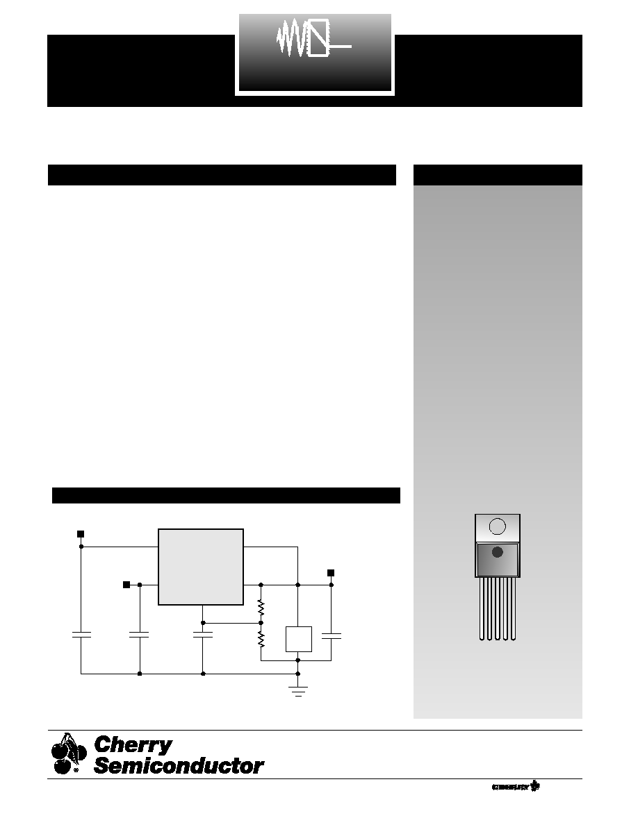
Applications Diagram
V
SENSE
V
OUT
V
CONTROL
V
POWER
CS52510-1
2.5V@10A
300
mF
5V
Load
124
1%
124
1%
0.1
mF
5V
100
mF
5V
10
mF
10V
3.3V
5.0V
Adjust
CS52510-1
2
Absolute Maximum Ratings
V
POWER
Input Voltage . . . . . . . . . . . . . . . . . . . . . . . . . . . . . . . . . . . . . . . . . . . . . . . . . . . . . . . . . . . . . . . . . . . . . . . . . . . . . . . . . . 6V
V
CONTROL
Input Voltage . . . . . . . . . . . . . . . . . . . . . . . . . . . . . . . . . . . . . . . . . . . . . . . . . . . . . . . . . . . . . . . . . . . . . . . . . . . . . . . 13V
Operating Junction Temperature Range . . . . . . . . . . . . . . . . . . . . . . . . . . . . . . . . . . . . . . . . . . . . . . . . . . . . . . . 0°C ≤ T
J
≤ 150°C
Storage Temperature Range . . . . . . . . . . . . . . . . . . . . . . . . . . . . . . . . . . . . . . . . . . . . . . . . . . . . . . . . . . . . . . . . . . -65°C to +150°C
Lead Temperature Soldering
Wave Solder (through hole styles only) . . . . . . . . . . . . . . . . . . . . . . . . . . . . . . . . . . . . . . . . . . . . 10 sec. max, 260°C peak
ESD Damage Threshold . . . . . . . . . . . . . . . . . . . . . . . . . . . . . . . . . . . . . . . . . . . . . . . . . . . . . . . . . . . . . . . . . . . . . . . . . . . . . . . . 2kV
Electrical Characteristics: 0°C ≤ T
A
≤ 70°C, 0°C ≤ T
J
≤ 150°C, V
SENSE
= V
OUT
and V
Adj
= 0V unless otherwise specified.
PARAMETER
TEST CONDITIONS
MIN
TYP
MAX
UNIT
Reference Voltage
V
CONTROL
= 2.75V to 12V, V
POWER
= 2.5V to 5.5V,
1.234
1.253
1.272
V
10mA ≤ I
OUT
≤ 10A
(-1.5%)
(+1.5%)
Line Regulation
V
CONTROL
= 2.5V to 12V, V
POWER
= 1.75V to 5.5V,
.02
.20
%
I
OUT
= 10mA
Load Regulation
V
CONTROL
= 2.75V, V
POWER
= 2.5V,
.04
.20
%
(Note 3)
I
OUT
= 10mA to 10A, with remote sense
Minimum Load Current
V
CONTROL
= 5V, V
POWER
= 3.3V, ∆V
OUT
= +1%
5
10
mA
(Note 1)
Control Pin Current
V
CONTROL
= 2.75V, V
POWER
= 2.5V, I
OUT
= 100mA
6
10
mA
(Note 2)
V
CONTROL
= 2.75V, V
POWER
= 2.5V, I
OUT
= 4A
30
60
mA
V
CONTROL
= 2.75V, V
POWER
= 1.75V, I
OUT
= 4A
33
70
mA
V
CONTROL
= 2.75V, V
POWER
= 2.5V, I
OUT
= 10A
80
180
mA
Adjust Pin Current
V
CONTROL
= 2.75V, V
POWER
=2.5V, I
OUT
= 10mA
60
120
µA
Current Limit
V
CONTROL
= 2.75V, V
POWER
= 2.5V, ∆V
OUT
= -1.5%
10.1
11.0
A
Short Circuit Current
V
CONTROL
= 2.75V, V
POWER
= 2.5V, V
OUT
= 0V
8.0
9.5
A
Ripple Rejection
V
CONTROL
= V
POWER
= 3.25V Avg,
60
80
dB
(Note 3)
V
RIPPLE
= 1V
P-P
@120Hz, I
OUT
= 4A, C
ADJ
= 0.1µF
Thermal Regulation
30ms Pulse, T
A
= 25°C
0.002
%/W
V
CONTROL
Dropout Voltage
V
POWER
= 2.5V, I
OUT
= 100mA
1.00
1.15
V
(Minimum V
CONTROL
-V
OUT
)
V
POWER
= 2.5V, I
OUT
= 1A
1.00
1.15
V
(Note 4)
V
POWER
= 2.5V, I
OUT
= 2.75A
1.00
1.15
V
V
POWER
= 2.5V, I
OUT
= 4A
1.00
1.15
V
V
POWER
= 2.5V, I
OUT
= 10A
1.25
1.40
V
V
POWER
Dropout Voltage
V
CONTROL
= 2.75V, I
OUT
= 100mA
.10
.15
V
(Minimum VPOWER-V
OUT
)
V
CONTROL
= 2.75V, I
OUT
= 1A
.15
.20
V
(Note 4)
V
CONTROL
= 2.75V, I
OUT
= 2.75A
.20
.30
V
V
CONTROL
= 2.75V, I
OUT
= 4A
.26
.40
V
V
CONTROL
= 2.75V, I
OUT
= 10A
.65
.80
V
RMS Output Noise
Freq = 10Hz to 10kHz, T
A
= 25°C
0.003
%V
OUT
Temperature Stability
0.5
%
Thermal Shutdown (Note 5)
150
180
210
°C
Thermal Shutdown Hysteresis
25
°C
V
CONTROL
Supply Only
V
CONTROL
= 13V, V
POWER
not connected,
50
mA
Output Current
V
ADJUST
= V
OUT
= V
SENSE
= 0V
CS52510-1
Package Pin Description
PACKAGE PIN #
PIN SYMBOL
FUNCTION
3
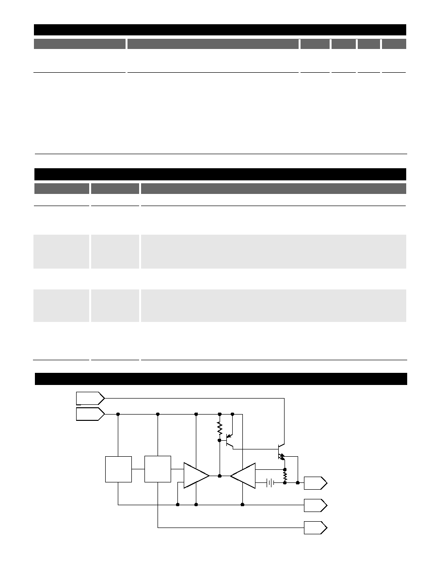
Block Diagram
V
POWER
V
CONTROL
BIAS
and
TSD
V
REF
EA
IA
V
OUT
V
SENSE
Adjust
-
+
-
+
Electrical Characteristics: 0°C≤T
A
≤ 70°C, 0°C≤T
J
≤ 150°C, V
SENSE
= V
OUT
and V
Adj
= 0V unless otherwise specified.
PARAMETER
TEST CONDITIONS
MIN
TYP
MAX
UNIT
V
POWER
Supply Only
V
POWER
= 6V, V
CONTROL
not connected,
0.1
1
mA
Output Current
V
ADJUST
= V
OUT
= V
SENSE
= 0V
Note 1:
The minimum load current is the minimum current required to maintain regulation. Normally the current in the resistor
divider used to set the output voltage is selected to meet the minimum load current requirement.
Note 2:
The control pin current is the drive current required for the output transistor. This current will track output current with
roughly a 1:100 ratio. The minimum value is equal to the quiescent current of the device.
Note 3:
This parameter is guaranteed by design and is not 100% production tested.
Note 4:
Dropout is defined as either minimum control voltage (V
CONTROL
) or minimum power voltage (V
POWER)
to output voltage dif-
ferential required to maintain 1.5% regulation at a particular load.
Note 5:
This parameter is guaranteed by design, but not parametrically tested in production. However, a 100% thermal shutdown
functional test is performed on each part.
5L TO-220
1
V
SENSE
This Kelvin sense pin allows for remote sensing of the output voltage at the load
for improved regulation. It is internally connected to the positive input of the
voltage sensing error amplifier.
2
Adjust
This pin is connected to the low side of the internally trimmed 1.5% bandgap refer-
ence voltage and carries a bias current of about 50µA. A resistor divider from Adj
to V
OUT
and from Adj to ground sets the output voltage. Also, transient response
can be improved by adding a small bypass capacitor from this pin to ground.
3
V
OUT
This pin is connected to the emitter of the power pass transistor and provides a
regulated voltage capable of sourcing 10A of current.
4
V
CONTROL
This is the supply voltage for the regulator control circuitry. For the device to
regulate, this voltage should be between 1V and 1.4V (depending on the output
current) greater than the output voltage. The control pin current will be about 1%
of the power pin output current .
5
V
POWER
This is the power input voltage. This pin is physically connected to the collector of
the power pass transistor. For the device to regulate, this voltage should be
between 0.1V and .8V greater than the output voltage depending on output cur-
rent. The output load current of 10A is supplied through this pin.
CS52510-1
4
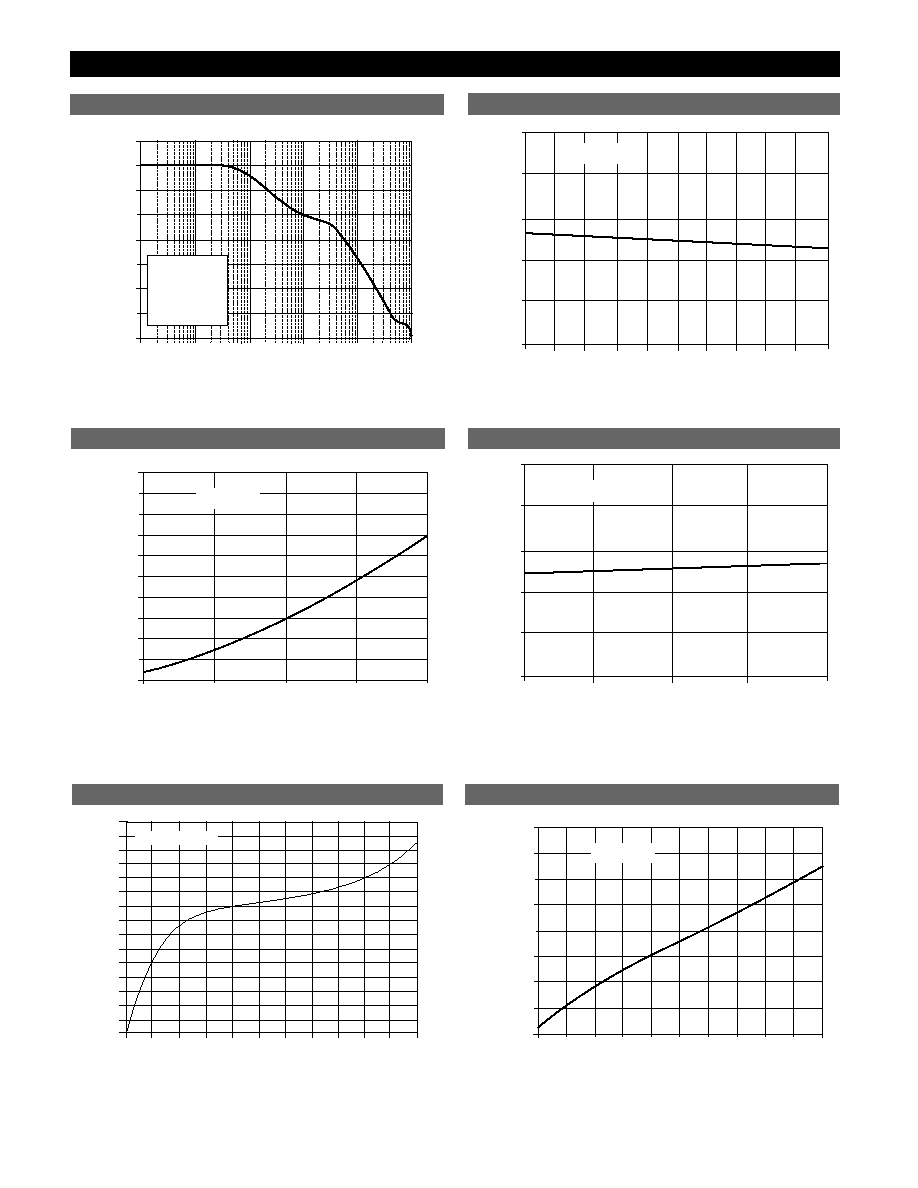
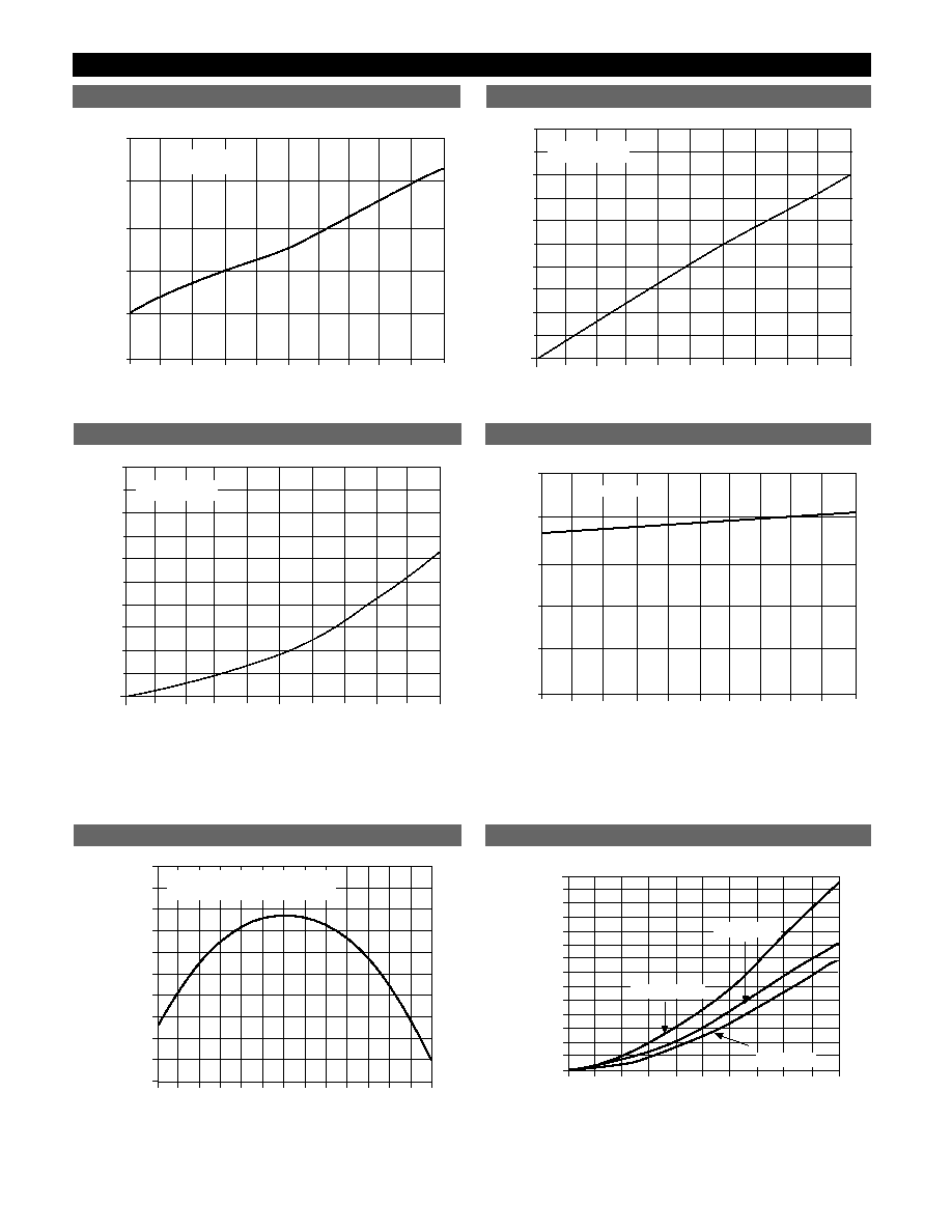
Typical Performance Characteristics
Ripple Rejection vs Frequency
Adjust Pin Current vs V
POWER
-V
OUT
0.0
0.5
0.0
15.0
Output Current (A)
V
POWER
-V
OUT
(V)
1.0
1.5
2.0
2.5
3.0
3.5
4.0
4.5
5.0
5.5
14.0
13.0
12.0
6.0
5.0
4.0
3.0
2.0
1.0
11.0
10.0
7.0
8.0
9.0
V
CONTROL
=2.75V
Short Circuit Current vs V
POWER
-V
OUT
Minimum Load Current vs V
POWER
-V
OUT
1.0
3.0
4.0
5.0
6.0
7.0
800.000
Minimum Load Curent (
m
A)
V
CONTROL
-V
OUT
(V)
9.0
10.0
11.0
2.0
8.0
850.000
900.000
950.000
1000.000
1050.000
1100.000
1150.000
1200.000
V
POWER
=3.3V
D V
OUT
=+1%
Minimum Load Current vs V
CONTROL
-V
OUT
Adjust Pin Current vs V
CONTROL
-V
OUT
10.0
10
1
Frequency (Hz)
Ripple Rejection (dB)
20.0
30.0
40.00
60.0
70.0
80.0
90.0
10
2
10
3
10
4
10
6
10
5
50.0
V
IN
-V
OUT
=2V
I
OUT
=4A
V
RIPPLE
=1V
P-P
C
OUT
=22
mF
C
ADJ
=0.1
mF
1.0
3.0
4.0
5.0
6.0
7.0
70.00
Adjust Pin Current (
m
A)
V
CONTROL
-V
OUT
(V)
9.0
71.00
72.00
73.00
74.00
75.00
10.0
11.0
2.0
8.0
V
POWER
=2.5V
IL=10mA
0.50
1.50
2.50
915.500
Minimum Load Current (
m
A)
V
POWER
-V
OUT
(V)
3.50
4.50
915.600
915.700
915.800
915.900
916.000
916.100
916.200
916.400
V
CONTROL
=5V
D V
OUT
=+1%
915.400
916.300
0.50
70.00
Adjust Pin Current (
m
A)
V
POWER
-V
OUT
(V)
2.50
71.00
72.00
73.00
74.00
75.00
3.50
4.50
1.50
V
CONTROL
=2.75V
IL=10mA
CS52510-1
Typical Performance Characteristics: continued
Load Regulation vs Output Current
Adjust Pin Current vs Output Current
V
CONTROL
Dropout Voltage vs I
OUT
V
POWER
Dropout Voltage vs I
OUT
5
0
10 20 30 40 50 60 70 80 90 100 110120130
-0.150
-0.125
-0.100
-0.075
-0.050
-0.025
-0.000
0.025
0.050
0.075
0.100
I
0
=10mA
V
CONTROL
=2.75V, V
POWER
=2.5V
T
J
(
∞
C)
Output V
oltage Deviation (%)
0.00
2.00
4.00
6.00
8.00
10.00
0.000
0.050
0.150
0.200
0.300
Output Current (A)
Output V
oltage Deviation (%)
0.350
0.250
0.100
T
Case
=0
∞C
T
Case
=125
∞C
T
Case
=25
∞C
Load Regulation vs Output Current
Reference Voltage vs Temperature
0.00
2.00
3.00
4.00
5.00
6.00
72.00
Adjust Pin Current (
m
A)
Output Current (A)
8.00
73.00
74.00
75.00
76.00
77.00
9.00 10.00
1.00
7.00
V
POWER
=2.5V
V
CONTROL
=2.75V
3.00
2.00
0.00
0.000
0.060
0.070
0.080
0.090
0.100
Output Current (A)
Output V
oltage Deviation (%)
1.00
4.00
6.00
5.00
7.00
0.010
0.020
0.050
0.040
0.030
8.00
9.00
10.00
V
POWER
=2.5V
V
CONTROL
=2.75V
3.00
2.00
0.00
0.000
0.600
0.700
0.800
0.900
1.000
Output Current (A)
V
POWER
Dropout V
oltage (V)
1.00
4.00
6.00
5.00
7.00
0.100
0.200
0.500
0.400
0.300
8.00
9.00
10.00
V
POWER
=2.5V
V
CONTROL
=2.75V
0.00
2.00
3.00
4.00
5.00
6.00
0.000
V
CONTROL
Dropout V
oltage (V)
Output Current (A)
8.00
0.250
0.500
0.750
1.000
1.250
9.00 10.00
1.00
7.00
V
POWER
=2.5V
Typical Performance Characteristics: continued
CS52510-1
6
0.0
83.0
Adjust Pin Current (
m
A)
Temperature (C)
40.0
60.0
80.0
100.0
81.0
79.0
77.0
75.0
73.0
71.0
69.0
67.0
65.0
20.0
120.0
160.0
140.0
Adjust Pin Current vs Temperature
Application Notes
50
0
-50
-100
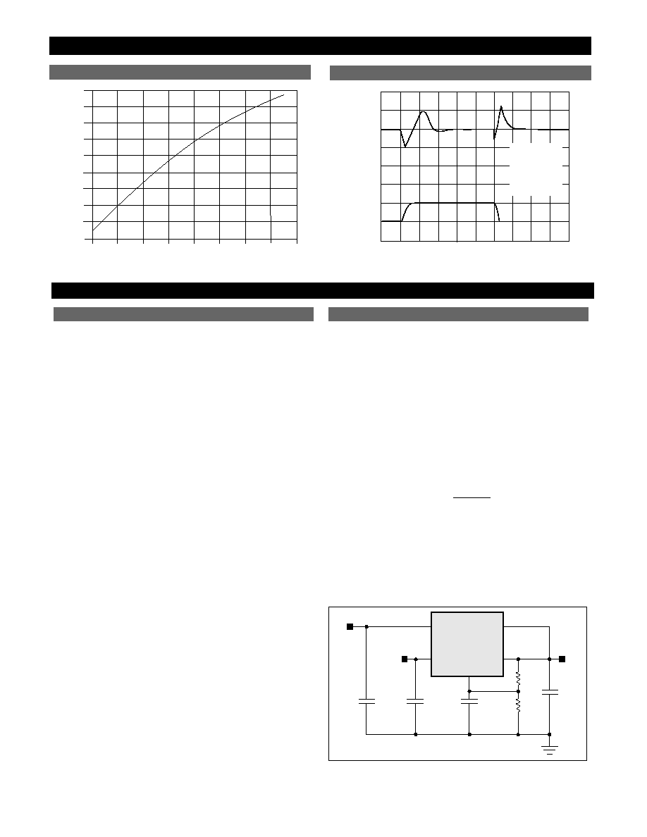
7
0
0
2
5
0
Time (
m
s)
Output V
oltage Deviation (mV)
Current (A)
100
1
3
4
C
OUT
=330
mF
C
POWER
=110
mF
C
CONTROL
=10
mF
C
ADJUST
=25
mF
V
CONTROL
=5V
V
POWER
=3.3V
V
OUT
=2.5V
Current Step Transient Response
The CS52510-1 linear regulator provides adjustable voltages
from 1.25V to 5V at currents up to 10A. The regulator is pro-
tected against short circuits, and includes a thermal shut-
down circuit with hysteresis. The output, which is current
limited, consists of a PNP-NPN transistor pair and requires
an output capacitor for stability. A detailed procedure for
selecting this capacitor is included in the Stability
Considerations section.
V
POWER
Function
The CS52510-1 utilizes a two supply approach to maximize
efficiency. The collector of the power device is brought out to
the V
POWER
pin to minimize internal power dissipation
under high current loads.V
CONTROL
provides power for the
control circuitry and the drive for the output NPN transistor.
V
CONTROL
should be at least 1V greater than the output volt-
age. Special care has been taken to ensure that there are no
supply sequencing problems. The output voltage will not
turn on until both supplies are operating. If the control volt-
age comes up first, the output current will be typically limit-
ed to about 3mA until the power input voltage comes up. If
the power input voltage comes up first the output will not
turn on at all until the control voltage comes up. The output
can never come up unregulated.
The CS52510-1 can also be used as a single supply device
with the control and power inputs tied together. In this
mode, the dropout will be determined by the minimum con-
trol voltage.
Output Voltage Sensing
The CS52510-1 five terminal linear regulator includes a dedi-
cated Vsense function. This allows for true Kelvin sensing of
the output voltage. This feature can virtually eliminate errors
in the output voltage due to load regulation. Regulation will
be optimized at the point where the sense pin is tied to the
output.
Adjustable Operation
This LDO adjustable regulator has an output voltage range
of 1.25V to 5V. An external resistor divider sets the output
voltage as shown in Figure 1. The regulator’s voltage sensing
error amplifier maintains a fixed 1.253V reference between
the output pin and the adjust pin.
A resistor divider network R
1
and R
2
causes a fixed current
to flow to ground. This current creates a voltage across R
2
that adds to the 1.253V across R1 and sets the overall output
voltage. The adjust pin current (typically 50µA) also flows
through R
2
and adds a small error that should be taken into
account if precise adjustment of V
OUT
is necessary. The out-
put voltage is set according to the formula:
V
OUT
= 1.253V
¥
+ R
2
¥ I
ADJ
The term I
ADJ
¥ R
2
represents the error added by the adjust
pin current.
R
1
is chosen so that the minimum load current is a least
10mA. R
1
and R
2
should be of the same composition for best
tracking over temperature. The divider resistors should be
placed as close to the load as possible.
Figure 1: An external resistor divider sets the value of V
OUT
. The 1.253V
reference voltage drops across R1.
V
SENSE
V
OUT
V
CONTROL
V
POWER
CS52510-1
R1
Adjust
R2
R
1
+ R
2
R
1
Design Guidelines
Theory of Operation
CS52510-1
7
Application Notes: continued
While not required, a bypass capacitor connected between
the adjust pin and ground will improve transient response
and ripple rejection. A 0.1µF tantalum capacitor is recom-
mended for “first cut” design. Value and type may be varied
to optimize performance vs. price.
Other Adjustable Operation Considerations
The CS52510-1 linear regulator has an absolute maximum
specification of 6V for the voltage difference between V
IN
and V
OUT
. However, the IC may be used to regulate voltages
in excess of 6V. The two main considerations in such a
design are the sequencing of power supplies and short cir-
cuit capability.
Power supply sequencing should be such that the V
CONTROL
supply is brought up coincidentally with or before the V
POW-
ER
supply. This allows the IC to begin charging output capac-
itor as soon as the V
POWER
to V
OUT
differential is large
enough that the pass transistor conducts. As V
POWER
increas-
es, the pass transistor will remain in dropout, and current is
passed to the load until V
OUT
is in regulation. Further
increase in the supply voltage brings the pass transistor out
of dropout. In this manner, any output voltage less than 13V
may be regulated, provided the V
POWER
to V
OUT
differential
is less than 6V. In the case where V
CONTROL
and V
POWER
are
shorted, there is no theoretical limit to the regulated voltage
as long as the V
POWER
to V
OUT
differential of 6V is not
exceeded.
There is a possibility of damaging the IC when V
POWER
-V
IN
is greater than 6V if a short circuit occurs. Short circuit condi-
tions will result in the immediate operation of the pass tran-
sistor outside of its safe operating area. Over-voltage stresses
will then cause destruction of the pass transistor before over-
current or thermal shutdown circuitry can become active.
Additional circuitry may be required to clamp the V
POWER
to
V
OUT
differential to less than 6V if fail safe operation is
required. One possible clamp circuit is illustrated in Figure 2;
however, the design of clamp circuitry must be done on an
application by application basis. Care must be taken to
ensure the clamp actually protects the design. Components
used in the clamp design must be able to withstand the short
circuit condition indefinitely while protecting the IC.
Figure 2: Example clamp circuitry for V
POWER
- V
OUT
> 6V.
Stability Considerations
The output compensation capacitor helps determine three
main characteristics of a linear regulator: start-up delay, load
transient response, and loop stability.
The capacitor value and type is based on cost, availability,
size and temperature constraints. A tantalum or aluminum
electrolytic capacitor is best, since a film or ceramic capacitor
with almost zero ESR can cause instability. The aluminum
electrolytic capacitor is the least expensive solution.
However, when the circuit operates at low temperatures,
both the value and ESR of the capacitor will vary consider-
ably. The capacitor manufacturers data sheet provides this
information.
A 300µF tantalum capacitor will work for most applications,
but with high current regulators such as the CS52510-1 the
transient response and stability improve with higher values
of capacitor. The majority of applications for this regulator
involve large changes in load current so the output capacitor
must supply the instantaneous load current. The ESR of the
output capacitor causes an immediate drop in output voltage
given by:
∆V = ∆I
¥ ESR.
For microprocessor applications it is customary to use an
output capacitor network consisting of several tantalum and
ceramic capacitors in parallel. This reduces the overall ESR
and reduces the instantaneous output voltage drop under
transient load conditions. The output capacitor network
should be as close to the load as possible for the best results.
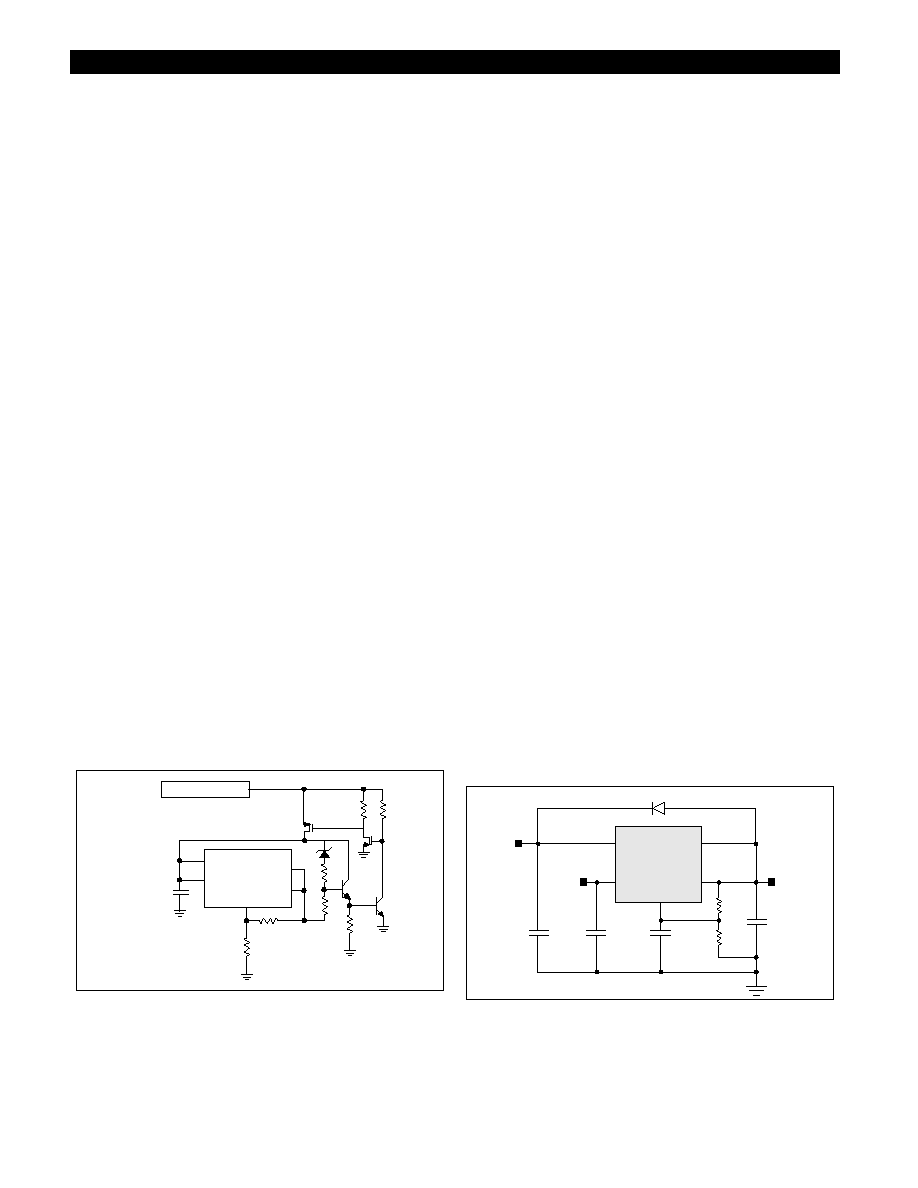
Protection Diodes
When large external capacitors are used with a linear regula-
tor it is sometimes necessary to add protection diodes. If the
input voltage of the regulator gets shorted, the output capac-
itor will discharge into the output of the regulator. The dis-
charge current depends on the value of the capacitor, the
output voltage, and the rate at which V
CONTROL
drops. In the
CS52510-1 regulator, the discharge path is through a large
junction and protection diodes are not usually needed. If the
regulator is used with large values of output capacitance and
the input voltage is instantaneously shorted to ground, dam-
age can occur. In this case, a diode connected as shown in
Figure 3 is recommended. Use of this diode has the added
benefit of bleeding V
OUT
to ground if V
CONTROL
is shorted.
This prevents an unregulated output from causing system
damage.
Figure 3: Diode protection against V
CONTROL
short circuit conditions.
V
SENSE
V
OUT
V
CONTROL
V
POWER
CS52510-1
Adjust
External Supply
V
Control
V
Power
V
Adjust
V
OUT
V
SENSE

8
CS52510-1
Application Notes: continued
A rule of thumb useful in determining if a protection diode is
required is to solve for current
I = C ¥ V ,
T
where
I
is the current flow out of the load capacitance
when V
CONTROL
is shorted,
C
is the value of load capacitance
V
is the output voltage, and
T
is the time duration required for V
CONTROL
to
transition from high to being shorted.
If the calculated current is greater than or equal to the typical
short circuit current value provided in the specifications, seri-
ous thought should be given to the use of a protection diode.
Current Limit
The internal current limit circuit limits the output current
under excessive load conditions.
Short Circuit Protection
The device includes short circuit protection circuitry that
clamps the output current at approximately two amperes less
than its current limit value. This provides for a current fold-
back function, which reduces power dissipation under a
direct shorted load.
Thermal Shutdown
The thermal shutdown circuitry is guaranteed by design to
become activate above a die junction temperature of approxi-
mately 150°C and to shut down the regulator output. This
circuitry has 25°C of typical hysteresis, thereby allowing the
regulator to recover from a thermal fault automatically.
Calculating Power Dissipation and Heat Sink
Requirements
High power regulators such as the CS52510-1 family usually
operate at high junction temperatures. Therefore, it is impor-
tant to calculate the power dissipation and junction tempera-
tures accurately to ensure that an adequate heat sink is used.
Since the package tab is connected to V
OUT
on the CS52510-1,
electrical isolation may be required for some applications.
Also, as with all high power packages, thermal compound is
necessary to ensure proper heat flow. For added safety, this
high current LDO includes an internal thermal shutdown cir-
cuit.
The thermal characteristics of an IC depend on the following
four factors: junction temperature, ambient temperature, die
power dissipation, and the thermal resistance from the die
junction to ambient air. The maximum junction temperature
can be determined by:
T
J(max)
= T
A(max)
+ PD
(max)
¥ R
QJA
The maximum ambient temperature and the power dissipa-
tion are determined by the design while the maximum junc-
tion temperature and the thermal resistance depend on the
manufacturer and the package type. The maximum power
dissipation for a regulator is:
PD
(max)
= (V
IN(max)
-V
OUT(min)
)I
OUT(max)
+ V
IN(max)
¥ I
IN(max)
A heat sink effectively increases the surface area of the pack-
age to improve the flow of heat away from the IC and into
the surrounding air. Each material in the heat flow path
between the IC and the outside environment has a thermal
resistance which is measured in degrees per watt. Like series
electrical resistances, these thermal resistances are summed
to determine the total thermal resistance between the die
junction and the surrounding air, R
QJA
. This total thermal
resistance is comprised of three components. These resistive
terms are measured from junction to case (R
QJC
), case to heat
sink R
QCS
), and heat sink to ambient air (R
QSA
). The equation
is:
R
QJA
= R
QJC
+ R
QCS
+ R
QSA
The value for R
QJC
is 1.4˚C/watt for the CS52510-1 in a
TO-220 package. For a high current regulator such as the
CS52510-1 the majority of heat is generated in the power
transistor section. The value for R
QSA
depends on the heat
sink type, while the R
QCS
depends on factors such as package
type, heat sink interface (is an insulator and thermal grease
used?), and the contact area between the heat sink and the
package. Once these calculations are complete, the maximum
permissible value of R
QJA
can be calculated and the proper
heat sink selected. For further discussion on heat sink selec-
tion, see our Cherry application note “Thermal Management
for Linear Regulators.”

9
PACKAGE THERMAL DATA
CS52510-1
Rev. 3/17/99
Package Specification
Ordering Information
Part Number
Description
CS52510-1GT5
5L TO-220 Straight
© 1999 Cherry Semiconductor Corporation
PACKAGE DIMENSIONS IN mm (INCHES)
Thermal Data
5L
TO-220
R
QJC
typ
1.4
˚C/W
R
QJA
typ
50
˚C/W
Cherry Semiconductor Corporation reserves the right to
make changes to the specifications without notice. Please
contact Cherry Semiconductor Corporation for the latest
available information.
5 Lead TO-220 (T) Straight
2.87 (.113)
2.62 (.103)
6.93(.273)
6.68(.263)
9.78 (.385)
10.54 (.415)
1.02(.040)
0.63(.025)
1.83(.072)
1.57(.062)
0.56 (.022)
0.36 (.014)
2.92 (.115)
2.29 (.090)
1.40 (.055)
1.14 (.045)
4.83 (.190)
4.06 (.160)
6.55 (.258)
5.94 (.234)
14.22 (.560)
13.72 (.540)
1.02 (.040)
0.76 (.030)
3.71 (.146)
3.96 (.156)
14.99 (.590)
14.22 (.560)