Features
s
1.25V to 5V V
OUT
at 8A
s
V
POWER
Dropout <0.4V @ 8A
s
V
CONTROL
Dropout <1.15V @
8A
s
1.5% Trimmed Reference
s
Fast Transient Response
s
Remote Voltage Sensing
s
Thermal Shutdown
s
Current Limit
s
Short Circuit Protection
s
Backwards Compatible with
3-pin Regulators
Package Options
CS5258-1
8A LDO 5-Pin Adjustable Linear Regulator
CS5258-1
Description
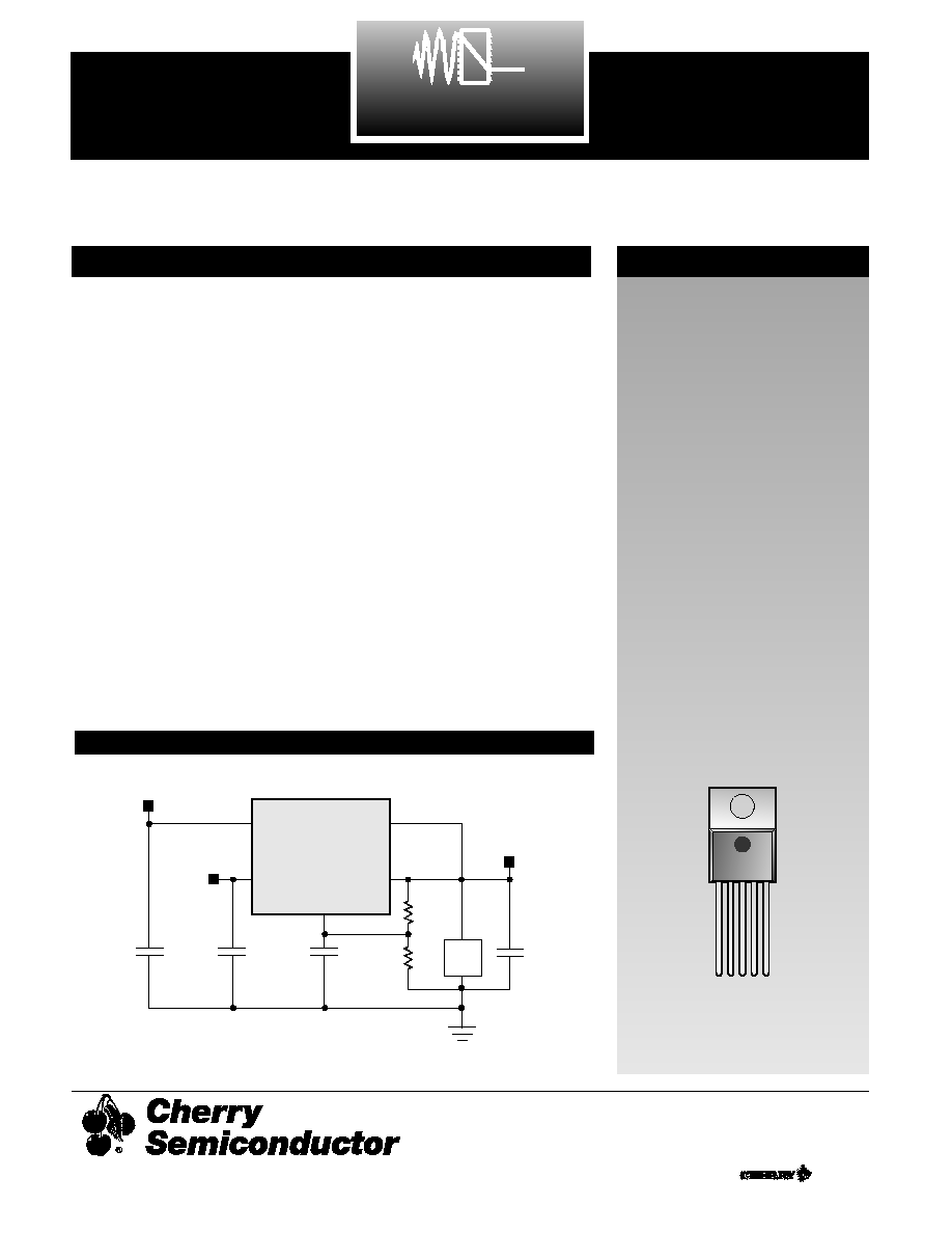
Applications Diagram
5 Lead TO-220
1
1. V
SENSE
2. Adjust
3. V
OUT
4. V
CONTROL
5. V
POWER
Tab = V
OUT
This new very low dropout regula-
tor is designed to power the next
generation of advanced microproces-
sors. To achieve very low dropout,
the internal pass transistor is pow-
ered separately from the control cir-
cuitry. Furthermore, with the control
and power inputs tied together, this
device can be used in single supply
configuration and still offer a better
dropout voltage than conventional
PNP-NPN based LDO regulators. In
this mode the dropout is determined
by the minimum control voltage.
It is supplied in a five-terminal TO-
220 package, which allows for the
implementation of a remote-sense
pin permitting very accurate regula-
tion of output voltage directly at the
load, where it counts, rather than at
the regulator. This remote sensing
feature virtually eliminates output
voltage variations due to load
changes and resistive voltage drops.
Typical load regulation measured at
the sense pin is 1mV for an output
voltage of 2.5V with a load step of
10mA to 8A.
The very fast transient loop response
easily meets the needs of the latest
microprocessors. In addition, a small
capacitor on the Adjust pin will fur-
ther improve the transient capabili-
ties.
Internal protection circuitry pro-
vides for �bust-proof� operation,
similar to three-terminal regulators.
This circuitry, which includes over-
current, short circuit, supply
sequencing and overtemperature
protection, will self protect the regu-
lator under all fault conditions.
The CS5258-1 is ideal for generating
a secondary 2 - 2.5V low voltage
supply on a motherboard where
both 5V and 3.3V are already
available.
V
SENSE
V
OUT
V
CONTROL
V
POWER
CS5258-1
2.5V@8A
300
mF
5V
Load
124
1%
124
1%
0.1
mF
5V
100
mF
5V
10
mF
10V
3.3V
5.0V
Adjust
1
A Company
�
Rev. 3/17/99
Cherry Semiconductor Corporation
2000 South County Trail, East Greenwich, RI 02818
Tel: (401)885-3600 Fax: (401)885-5786
Email: info@cherry-semi.com
Web Site: www.cherry-semi.com
PARAMETER
TEST CONDITIONS
MIN
TYP
MAX
UNIT
CS5258-1
2
Absolute Maximum Ratings
Reference Voltage
V
CONTROL
= 2.75V to 12V, V
POWER
= 2.15V to 5.5V,
1.234
1.253
1.272
V
10mA � I
OUT
� 8A
(-1.5%)
(+1.5%)
Line Regulation
V
CONTROL
= 2.5V to 12V, V
POWER
= 1.75V to 5.5V,
.02
.20
%
I
OUT
= 10mA
Load Regulation
V
CONTROL
= 2.75V, V
POWER
= 2.15V,
.04
.20
%
(Note 3)
I
OUT
= 10mA to 8A, with remote sense
Minimum Load Current
V
CONTROL
= 5V, V
POWER
= 3.3V, �V
OUT
= +1%
5
10
mA
(Note 1)
Control Pin Current
V
CONTROL
= 2.75V, V
POWER
= 2.15V, I
OUT
= 100mA
6
10
mA
(Note 2)
V
CONTROL
= 2.75V, V
POWER
= 2.15V, I
OUT
= 4A
30
60
mA
V
CONTROL
= 2.75V, V
POWER
= 1.75V, I
OUT
= 4A
33
70
mA
V
CONTROL
= 2.75V, V
POWER
= 2.15V, I
OUT
= 8A
80
180
mA
Adjust Pin Current
V
CONTROL
= 2.75V, V
POWER
= 2.15V, I
OUT
= 10mA
60
120
�A
Current Limit
V
CONTROL
= 2.75V, V
POWER
= 2.15V, �V
OUT
= -1.5%
8.1
10.0
A
Short Circuit Current
V
CONTROL
= 2.75V, V
POWER
= 2.15V, V
OUT
= 0V
6.0
9.0
A
Ripple Rejection
V
CONTROL
= V
POWER
= 3.25V Avg,
60
80
dB
(Note 3)
V
Ripple
= 1V
P-P
@ 120Hz, I
OUT
= 4A, C
ADJ
= 0.1�F
Thermal Regulation
30ms Pulse, T
A
= 25�C
0.002
%/W
V
CONTROL
Dropout Voltage
V
POWER
= 2.15V, I
OUT
= 100mA
1.00
1.15
V
(Minimum V
CONTROL
-V
OUT
)
V
POWER
= 2.15V, I
OUT
= 1A
1.00
1.15
V
(Note 4)
V
POWER
= 2.15V, I
OUT
= 2.75A
1.00
1.15
V
V
POWER
= 2.15V, I
OUT
= 4A
1.00
1.15
V
V
POWER
= 2.15V, I
OUT
= 8A
1.15
1.30
V
V
POWER
Dropout Voltage
V
CONTROL
= 2.75V, I
OUT
= 100mA
.10
.15
V
(Minimum V
POWER
-V
OUT
)
V
CONTROL
= 2.75V, I
OUT
= 1A
.15
.20
V
(Note 4)
V
CONTROL
= 2.75V, I
OUT
= 2.75A
.20
.30
V
V
CONTROL
= 2.75V, I
OUT
= 4A
.26
.40
V
V
CONTROL
= 2.75V, I
OUT
= 8A
.40
.70
V
RMS Output Noise
Freq = 10Hz to 10kHz, T
A
= 25�C
0.003
%V
OUT
Temperature Stability
0.5
%
Thermal Shutdown (Note 5)
150
180
210
�C
Thermal Shutdown Hysteresis
25
�C
V
CONTROL
Supply Only
V
CONTROL
= 13V, V
POWER
not connected,
50
mA
Output Current
V
ADJUST
= V
OUT
= V
SENSE
= 0V
Electrical Characteristics: 0�C � T
A
� 70�C, 0�C � T
J
� 150�C, V
SENSE
= V
OUT
and V
Adj
= 0V unless otherwise specified.
V
POWER
Input Voltage .................................................................................................................................................................6V
V
CONTROL
Input Voltage ...........................................................................................................................................................13V
Operating Junction Temperature Range...........................................................................................................0�C � T
J
� 150�C
Storage Temperature Range ................................................................................................................................-65�C to +150�C
ESD Damage Threshold............................................................................................................................................................2kV
Lead Temperature Soldering
Wave Solder (through hole styles only) .....................................................................................10 sec. max, 260�C peak
CS5258-1
PACKAGE PIN #
PIN SYMBOL
FUNCTION
3
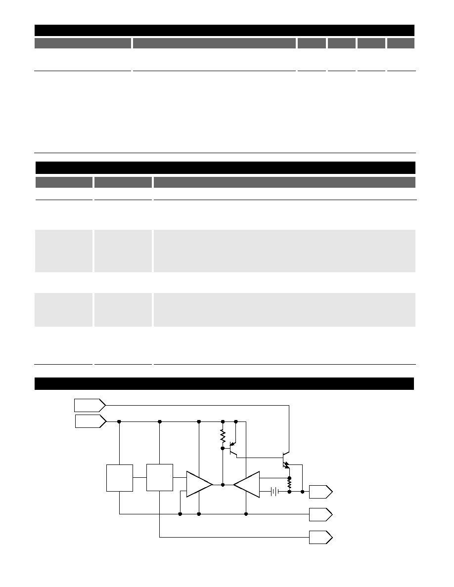
Block Diagram
V
POWER
V
CONTROL
BIAS
and
TSD
V
REF
EA
IA
V
OUT
V
SENSE
Adjust
-
+
-
+
Electrical Characteristics: 0�C � T
A
� 70�C, 0�C � T
J
� 150�C, V
SENSE
= V
OUT
and V
Adj
= 0V unless otherwise specified.
PARAMETER
TEST CONDITIONS
MIN
TYP
MAX
UNIT
V
POWER
Supply Only
V
POWER
= 6V, V
CONTROL
not connected,
0.1
1
mA
Output Current
V
ADJUST
= V
OUT
= V
SENSE
= 0V
Note 1:
The minimum load current is the minimum current required to maintain regulation. Normally the current in the resistor
divider used to set the output voltage is selected to meet the minimum load current requirement.
Note 2:
The control pin current is the drive current required for the output transistor. This current will track output
current with roughly a 1:100 ratio. The minimum value is equal to the quiescent current of the device.
Note 3:
This parameter is guaranteed by design and is not 100% production tested.
Note 4:
Dropout is defined as either minimum control voltage (V
CONTROL
) or minimum power voltage (V
POWER
) to output volt-
age differential required to maintain 1.5% regulation at a particular load current.
Note 5:
This parameter is guaranteed by design, but not parametrically tested in production. However, a 100% thermal shutdown
functional test is performed on each part.
Package Pin Description
5L TO-220
1
V
SENSE
This Kelvin sense pin allows for remote sensing of the output voltage at the
load for improved regulation. It is internally connected to the positive input of
the voltage sensing error amplifier.
2
Adjust
This pin is connected to the low side of the internally trimmed 1.5% bandgap
reference voltage and carries a bias current of about 50uA. A resistor divider
from Adj to V
OUT
and from Adj to ground sets the output voltage. Also, tran-
sient response can be improved by adding a small bypass capacitor from this
pin to ground.
3
V
OUT
This pin is connected to the emitter of the power pass transistor and provides
a regulated voltage capable of sourcing 8A of current.
4
V
CONTROL
This is the supply voltage for the regulator control circuitry. For the device to
regulate, this voltage should be between 1V and 1.30V (depending on the out-
put current) greater than the output voltage. The control pin current will be
about 1% of the output current .
5
V
POWER
This is the power input voltage. The pin is physically connected to the collec-
tor of the power pass transistor. For the device to regulate, this voltage should
be between 0.1V and .7V greater than the output voltage depending on output
current. The output load current of 8A is supplied through this pin.
CS5258-1
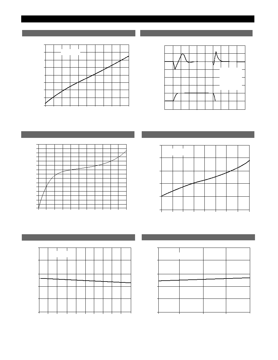
4
V
CONTROL
Dropout vs I
OUT
V
POWER
Dropout Voltage vs I
OUT
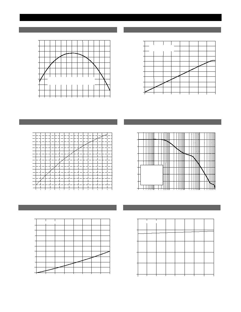
Typical Performance Characteristics
0 10
20 30
40
50 60 70 80
90 100 110 120 130
-0.150
-0.125
-0.100
-0.075
-0.050
-0.025
-0.000
0.025
0.050
0.075
0.100
I
0
=10mA
V
CONTROL
=2.75V, V
POWER
=2.15V
T
J
(
�
C)
Ooutput V
oltage Deviation (%)
0.00
8.00
0.000
Output Current (A)
Output V
oltage Deviation (%)
0.080
0.090
0.100
0.070
0.060
0.050
0.040
0.030
0.020
0.010
1.00
2.00
3.00
4.00
5.00
6.00
7.00
VPOWER=2.15V
VCONTROL=2.75V
Load Regulation vs Output Current
Reference Voltage vs Temperature
3.00
2.00
0.00
0.00
0.250
0.500
0.750
1.000
1.250
Output Current (A)
V
CONTROL
Drop Out V
oltage (V)
V
POWER
=2.15V
1.00
4.00
6.00
5.00
7.00
8.00
0.00
8.00
0.000
1.000
V
POWER
Dropout V
oltage (V)
Output Current
(A)
1.00
2.00
3.00
4.00
5.00
6.00
7.00
0.900
0.800
0.700
0.600
0.500
0.400
0.300
0.200
0.100
V
CONTROL
=2.75V
Ripple Rejection vs Frequency
Adjust Pin Current vs Temperature
10.0
10
1
Frequency (Hz)
Ripple Rejection (dB)
20.0
30.0
40.00
60.0
70.0
80.0
90.0
10
2
10
3
10
4
10
6
10
5
50.0
V
IN
-V
OUT
=2V
I
OUT
=4A
V
RIPPLE
=1V
P-P
C
OUT
=22
mF
C
ADJ
=0.1
mF
0.0
83.0
Adjust Pin Current (
m
A)
Temperature (C)
40.0
60.0
80.0
100.0
81.0
79.0
77.0
75.0
73.0
71.0
69.0
67.0
65.0
20.0
120.0
160.0
140.0
CS5258-1
Typical Performance Characteristics: continued
Current Step Transient Response
5
Minimum Load Current vs V
CONTROL
-V
OUT
50
0
-50
-100
8
0
0
2
5
0
Time (
m
s)
Output V
oltage Deviation (mV)
Current (A)
100
1
3
4
C
OUT
=330
mF
C
POWER
=110
mF
C
CONTROL
=10
mF
C
ADJUST
=0.1
mF
V
CONTROL
=5V
V
POWER
=3.3V
V
OUT
=2.5V
1.0
3.0
4.0
5.0
6.0
7.0
800.000
Minimum Load Current (
m
A)
V
CONTROL
-V
OUT
(V)
9.0
10.0
11.0
2.0
8.0
850.000
900.000
950.000
1000.000
1050.000
1100.000
1150.000
1200.000
V
POWER
= 3.3V
D V
OUT
= +1%
74.00
76.00
77.00
0.00
1.00
5.00
7.00
Output Current (A)
Adjust Pin Current (
m
A)
75.00
73.00
72.00
6.00
2.00
3.00
4.00
8.00
V
POWER
=2.15
V
CONTROL
=2.75V
Adjust Pin Current vs Output Current
0.0
0.5
0.0
15.0
Output Current (A)
V
POWER
-V
OUT
(V)
1.0
1.5
2.0
2.5
3.0
3.5
4.0
4.5
5.0
5.5
14.0
13.0
12.0
6.0
5.0
4.0
3.0
2.0
1.0
11.0
10.0
7.0
8.0
9.0
Short Circuit Current vs V
POWER
-V
OUT
1.0
3.0
4.0
5.0
6.0
7.0
70.00
Adjust Pin Current (
m
A)
V
CONTROL
-V
OUT
(V)
9.0
71.00
72.00
73.00
74.00
75.00
10.0
11.0
2.0
8.0
V
POWER
=2.15V
IL=10mA
Adjust Pin Current vs V
CONTROL
-V
OUT
0.50
70.00
Adjust Pin Current (
m
A)
V
POWER
-V
OUT
(V)
2.50
71.00
72.00
73.00
74.00
75.00
3.50
4.50
1.50
V
CONTROL
=2.75V
IL=10mA
Adjust Pin Current vs V
POWER
-V
OUT