Features
V
BAT
42.5
mH
10
mF
C
FLT
.25
mF
R
OSC
C
OSC
390pF
OUTPUT
Gnd
INH
FLT
R
OSC
I
ADJ
I
SENSE+
NC
V
REG
C
OSC
CTL
PGnd
V
CC
P1
N1
10K
100K
10K
10K
10K
R
CS1
51
R
CS2
51
C
CS
.022
mF
10K
10K
Input
1000
mF
MOT+
R
SENSE
4m
W
105K
MOT-
1000
mF
R
S
51
R
GATE
6
10
mF
.01
mF
1M
I
SENSE-
s
200 mA Peak PWM Gate
Drive Output
s
Patented Voltage
Compensation Circuit
s
100% Duty Cycle
Capability
s
5V, ± 3% Linear Reg.
s
Low Current Sleep Mode
s
Overvoltage Protection
s
Over Current Protection
of External MOSFET /
IGBT
s
Output Inhibit
Package Options
CS7054
Low Side PWM FET Controller
CS7054
Description
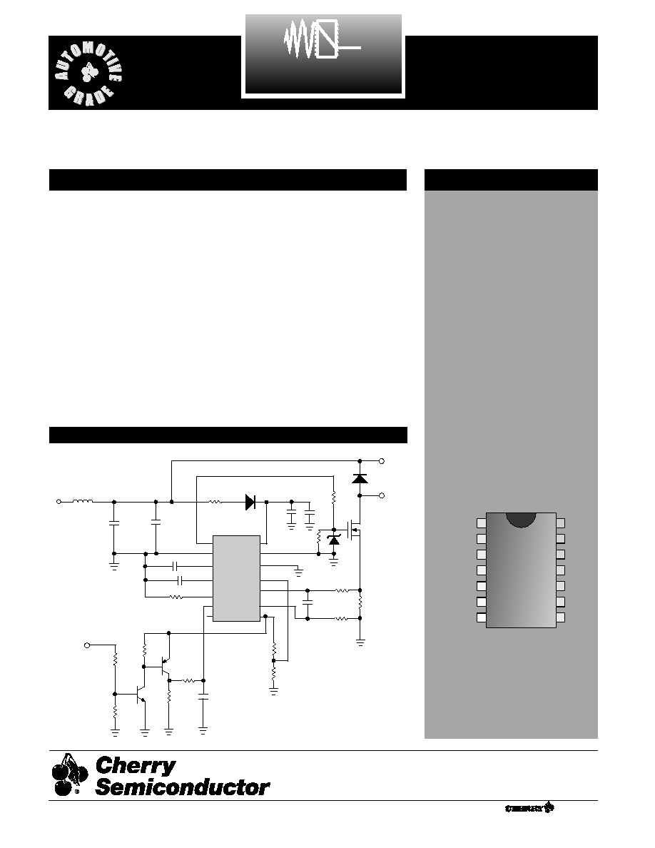
The CS7054 is a monolithic integrat-
ed circuit designed primarily to
control the rotor speed of perma-
nent magnet, direct current (DC)
brush motors. It drives the gate of
an N channel power MOSFET or
IGBT with a user-adjustable, fixed
frequency, variable duty cycle,
pulse width modulated (PWM) sig-
nal. The CS7054 can also be used to
control other loads such as incan-
descent bulbs and solenoids.
Inductive current from the motor or
solenoid is recirculated through an
external diode.
The CS7054 accepts a DC level
input signal of 0 to 5V to control the
pulse width of the output signal.
This signal can be generated by a
potentiometer referenced to the on-
chip 5V linear regulator, or a fil-
tered 0% to 100% PWM signal also
referenced to the 5V regulator.
The IC is placed in a sleep state by
pulling the CTL lead below 0.5V. In
this mode everything on the chip is
shut down except for the on-chip
regulator and the overall current
draw is less than 275 µA. There are
a number of on-chip diagnostics
that look for potential failure modes
and can disable the external power
MOSFET.
Application Diagram
1
OUTPUT
2
3
4
5
6
7
Gnd
FLT
R
OSC
CTL
NC
14
13
12
11
10
V
CC
PGnd
INH
I
ADJ
V
REG
8
9
C
OSC
I
SENSE+
I
SENSE-
14 Lead PDIP
1
Consult factory for 16 lead SO
wide package.
Cherry Semiconductor Corporation
2000 South County Trail, East Greenwich, RI 02818
Tel: (401)885-3600 Fax: (401)885-5786
Email: info@cherry-semi.com
Web Site: www.cherry-semi.com
A Company
®
Rev. 4/21/99
CS7054
2
Storage Temperature ................................................................................................................................................-65˚C to 150˚C
V
CC
................................................................................................................................................................................-0.3V to 30V
Supply Voltage Range (load dump = 26Vw/series 51Ω resistor) V
CC
Peak Transient Voltage.....................................40V
Input Voltage Range (at any input) ...........................................................................................................................-0.3V to 10V
Maximum Junction Temperature ..........................................................................................................................................150˚C
ESD Capability (Human Body Model) ....................................................................................................................................2kV
Lead Temperature Soldering: Wave Solder (through hole styles only)..........................................10 sec. max, 260°C peak
Absolute Maximum Ratings
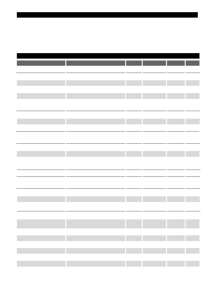
Electrical Characteristics:
8V < V
CC
< 16V, -40˚C < T
A
< 125°C, (unless otherwise specified)
PARAMETER
TEST CONDITIONS
MIN
TYP
MAX
UNIT
s V
CC
Supply
Operating Current Supply
5
10
mA
Quiescent Current
V
CC
= 12V
170
275
µA
Overvoltage Shutdown
18
19.5
21
V
Overvoltage Hysteresis
150
325
500
mV
s Control (CTL)
Control Input Current
CTL = 0V to 5V
-2
0.1
2
µA
Sleep Mode Threshold
8%
10%
12%
V
REG
Sleep Mode Hysteresis
50
100
150
mV
s Current Sense
Differential Voltage Sense
I
ADJ
=51.2% V
REG
and R
CS1
= 51Ω
60.5
79.5
mV
I
ADJ
Input Current
I
ADJ
= 0V to 5V
-5
0.3
2
µA
s Linear Regulator V
REG
Output Voltage
V
CC
= 13.2V
4.85
5.00
5.15
V
s Inhibit
Inhibit Threshold
40%
50%
60%
V
REG
Inhibit Hysteresis
150
325
500
mV
s External Drive (OUTPUT)
Output Frequency
R
OSC
= 105kΩ, C
OSC
= 390pF
17
20
23
kHz
Voltage to Duty Cycle
V
CC
= 13V, CTL = 30% V
REG
26.3
38.5
%
Conversion
V
CC
= 13V, CTL = 70% V
REG
69.5
81.5
%
Output Rise Time
V
CC
= 13V, R
GATE
= 6Ω, C
GATE
= 5nF
.25
1
µs
Output Fall Time
V
CC
= 13V, R
GATE
= 6Ω, C
GATE
= 5nF
.30
1
µs
Output Sink Current
V
CC
= 13V, R
GATE
= 6Ω, C
GATE
= 5nF
400
mA
Output Source Current
V
CC
= 13V, R
GATE
= 6Ω, C
GATE
= 5nF
400
mA
Output High Voltage
I
OUT
= 1mA
V
CC
- 1.7
V
Output Low Voltage
I
OUT
= -1mA
1.3
V

CS7054
3
Package Lead Description
PACKAGE LEAD #
LEAD SYMBOL
FUNCTION
Application Information
Oscillator
The IC sets up a constant frequency triangle wave at the
C
OSC
lead whose frequency is determined by the external
components R
OSC
and C
OSC
by the following equation:
Frequency =
The peak and valley of the triangle wave are proportional
to V
CC
by the following:
V
VALLEY
= 0.2
¥ V
CC
V
PEAK
= 0.8
¥ V
CC
This is required to make the voltage compensation func-
tion properly. In order to keep the frequency of the oscilla-
tor constant the current that charges C
OSC
must also vary
with supply. R
OSC
sets up the current which charges C
OSC
.
The voltage across R
OSC
is 50% of V
CC
and therefore:
I
ROSC
= 0.5
¥
I
ROSC
is multiplied by two (2) internally and transferred to
the C
OSC
lead. Therefore:
I
COSC
= ±
The period of the oscillator is:
T = 2C
OSC
¥
The R
OSC
and C
OSC
components can be varied to create fre-
quencies over the range of 15Hz to 25kHz. With the sug-
gested values of 105kΩ and 390pF for R
OSC
and C
OSC
respectively, the nominal frequency will be approximately
20 kHz. I
ROSC
, at V
CC
= 14V, will be 66.7 µA. I
ROSC
should
not change over a more than 2:1 ratio and therefore C
OSC
should be changed to adjust the oscillator frequency.
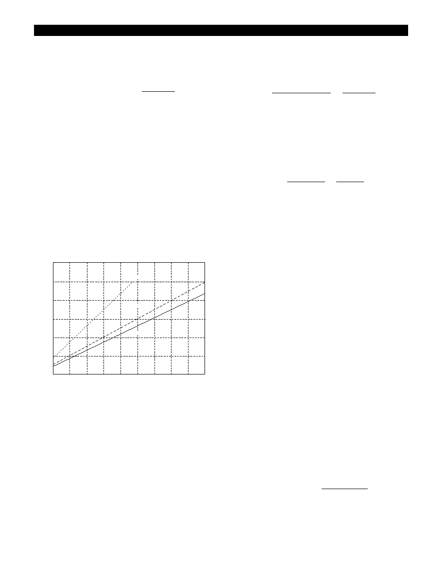
Voltage Duty Cycle Conversion
The IC translates an input voltage at the CTL lead into a
duty cycle at the OUTPUT lead. The transfer function
incorporates Cherry Semiconductor’s patented Voltage
Compensation method to keep the average voltage and
current across the load constant regardless of fluctuations
(V
PEAK
- V
VALLEY
)
I
COSC
V
CC
R
OSC
V
CC
R
OSC
0.83
R
OSC
¥ C
OSC
Theory Of Operation
14 Lead PDIP
1
OUTPUT
MOSFET Gate Drive
2
Gnd
Ground
3
FLT
Fault time out capacitor
4
C
OSC
Oscillator capacitor
5
R
OSC
Oscillator resistor
6
CTL
Pulse width control input
7
NC
No connection
8
V
REG
5V linear regulator
9
I
SENSE-
Current sense minus
10
I
SENSE+
Current sense plus
11
I
ADJ
Current limit adjust
12
INH
Output Inhibit
13
PGnd
Power ground for on chip clamp
14
V
CC
Positive power supply input
CS7054
4
Application Information: continued
in the supply voltage. The duty cycle is varied based upon
the input voltage and supply voltage by the following
equation:
Duty Cycle = 100%
¥
An internal DC voltage equal to:
V
DC
= (1.683
¥ V
CTL
) + (V
VALLEY
)
is compared to the oscillator voltage to produce the com-
pensated duty cycle. The transfer is set up so that at V
CC
=
14V the duty will equal V
CTL
divided by V
REG
. For exam-
ple at V
CC
= 14V, V
REG
= 5V and V
CTL
= 2.5V, the duty
cycle would be 50% at the output. This would place a 7V
average voltage across the load. If V
CC
then drops to 10V,
the IC would change the duty cycle to 70% and hence keep
the average load voltage at 7V.
Figure 1: Voltage Compensation
5V Linear Regulator
There is a 5V, 5mA linear regulator available at the V
REG
lead for external use. This voltage acts as a reference for
many internal and external functions. It has a drop out of
approximately 1.5V at room temperature and does not
require an external capacitor for stability.
Current Sense and Timer
The IC differentially monitors the load current on a cycle
by cycle basis at the I
SENSE+
and I
SENSE-
leads. The differen-
tial voltage across these two leads is amplified internally
and compared to the voltage at the I
ADJ
lead. The gain, A
V
,
is set internally and externally by the following equation:
A
V
=
=
The current limit (I
LIM
) is set by the external current sense
resistor (R
SENSE
) placed across the I
SENSE+
and I
SENSE-
ter-
minals and the voltage at the I
ADJ
lead.
I
LIM
=
¥
The R
CS
resistors and C
CS
components form a differential
low pass filter which filters out high frequency noise gen-
erated by the switching of the external MOSFET and the
associated lead noise. R
CS
also forms an error term in the
gain of the I
LIM
equation because the I
SENSE+
and I
SENSE-
leads are low impedance inputs thereby creating a good
current sensing amplifier. Both leads source 50µA while
the chip is in run mode. R
CS
should be much less than 1000
Ω to minimize error in the I
LIM
equation. I
ADJ
should be
biased between 1V and 4V.
When the current through the external MOSFET exceeds
I
LIM
, an internal latch is set and the output pulls the gate of
the MOSFET low for the remainder of the oscillator cycle
(fault mode). At the start of the next cycle, the latch is reset
and the IC reverts back to run mode until another fault
occurs. If a number of faults occur in a given period of
time, the IC “times out” and disables the MOSFET for a
long period of time to let it cool off. This is accomplished
by charging the C
FLT
capacitor each time an over current
condition occurs. If a cycle goes by with no overcurrent
fault occurring, an even smaller amount of charge will be
removed from C
FLT
. If enough faults occur together, even-
tually C
FLT
will charge up to 2.4V and the fault latch will
be set. The fault latch will not be reset until the C
FLT
dis-
charges to 0.6V. This action will continue indefinitely if the
fault persists.
The off time and on time are set by the following:
Off Time = C
FLT
¥
2.4V - 0.6V
4.5µA
V
I(ADJ)
R
SENSE
(1000 + R
CS
)
37000
37000
1000 + R
CS
V
I(ADJ)
I
SENSE+
- I
SENSE-
120%
100%
80%
60%
40%
20%
0%
10%
20%
30%
40%
50%
60%
70%
80%
90%
100%
CTL Voltage (% of V
REG
)
Duty Cycle( %)
V
CC
= 8V
V
CC
= 14V
V
CC
= 16V
2.8
¥ V
CTL
V
CC

CS7054
5
Application Information: continued
On Time = C
FLT
¥
where:
I
AVG
= (295.5µA
¥ DC) - [4.5µA ¥ (1 - DC)]
I
AVG
= (300µA
¥ DC) - 4.5µA
DC = PWM Duty Cycle
Sleep State
This device will enter into a low current mode (<275µA)
when CTL lead is brought to less than 0.5V. All functions
are disabled in this mode, except for the regulator.
Inhibit
When the inhibit voltage is greater than 2.5V the internal
latch is set and the external MOSFET will be turned off for
the remainder of the oscillator cycle. The latch is then reset
at the start of the next cycle.
Overvoltage Shutdown
The IC will disable the output during an overvoltage
event. This is a real time fault event and does not set the
internal latch and therefore is independent of the oscillator
timing (i.e. asynchronous). There is no undervoltage lock-
out. The device will shutdown gracefully once it runs out
of headroom.
Reverse Battery
The CS7054 will not survive a reverse battery condition.
Therefore, a series diode is required between the battery
and the V
CC
lead.
Load Dump
V
CC
is internally clamped to 30V. It is recommended that a
51Ω resistor, (R
S
) is placed in series with V
CC
to limit the
current flow into the IC in the event of a 40V peak tran-
sient condition.
2.4V - 0.6V
I
AVG
Thermal Data
14L
PDIP
R
QJC
typ
48
˚C/W
R
QJA
typ
85
˚C/W
6
Rev. 4/21/99
© 1999 Cherry Semiconductor Corporation
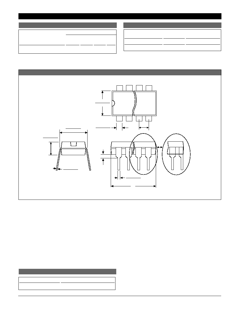
Package Specification
PACKAGE DIMENSIONS IN mm (INCHES)
D
Lead Count
Metric
English
Max
Min
Max
Min
14L PDIP
19.69
18.67
.775
.735
PACKAGE THERMAL DATA
CS7054
Ordering Information
Part Number
Description
CS7054YN14
14 Lead PDIP
Cherry Semiconductor Corporation reserves the
right to make changes to the specifications without
notice. Please contact Cherry Semiconductor
Corporation for the latest available information.
Plastic DIP (N); 300 mil wide
0.39 (.015)
MIN.
2.54 (.100) BSC
1.77 (.070)
1.14 (.045)
D
Some 8 and 16 lead
packages may have
1/2 lead at the end
of the package.
All specs are the same.
.203 (.008)
.356 (.014)
REF: JEDEC MS-001
3.68 (.145)
2.92 (.115)
8.26 (.325)
7.62 (.300)
7.11 (.280)
6.10 (.240)
.356 (.014)
.558 (.022)