1
Features
Over
Voltage
Shutdown
RESET
Comparator
Error
Amplifier
+
-
TO V
OUT
+
+
-
VREF
ENABLE
Comparator
Bandgap
Supply
Output
Current
Limit
Bandgap
Reference
Thermal
Shutdown
-
V
IN
ENABLE
RESET
V
OUT
Gnd
s
5V ± 4% Output Voltage
300mA
s
Low Dropout Voltage
(1V @ 150mA)
s
Low Quiescent Current
(2.5mA @ I
OUT
= 150mA)
s
µP Compatible Control
Functions
s
Low Current Sleep Mode
I
Q
=250µA
s
Fault Protection
Thermal Shutdown
Short Circuit
60V Load Dump
ENABLE
RESET
Package Options
5 Lead TO-220
Tab (Gnd)
14 Lead SOIC
Narrow
8 Lead PDIP
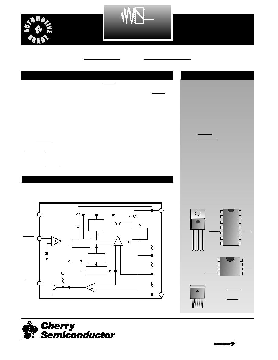
CS8120
5V, 300mA Linear Regulator with
and ENABLE
RESET
1
CS8120
Description
The CS8120 is a 5V, 300mA precision
linear regulator with two microproces-
sor compatible control functions and
protection circuitry included on chip.
The composite NPN-PNP output pass
transistor assures a lower dropout volt-
age (1V @ 200mA) without requiring
excessive supply current (2.5mA).
The CS8120’s two logic control func-
tions make this regulator well suited to
applications requiring microprocessor-
based control at the board or module
level.
controls the output
stage. A high voltage (>2.9V) on the
lead turns off the regula-
tor’s pass transistor and sends the IC
into Sleep mode where it draws only
250µA. The
function sends a
signal when the IC is power-
ing up or whenever the output voltage
moves out of regulation. The
signal is valid down to V
OUT
= 1V.
The CS8120 design optimizes supply
rejection by switching the internal
bandgap reference from the supply
input to the regulator output as soon as
the nominal output voltage is achieved.
Additional on chip filtering enhances
rejection of high frequency transients
on all external leads.
The CS8120 is fault protected against
short circuit, over voltage and thermal
runaway conditions.
RESET
RESET
RESET
ENABLE
ENABLE
Block Diagram *
1
V
IN
SENSE
NC
V
OUT
Gnd
NC
NC
NC
NC
NC
NC
NC
RESET
ENABLE
1
V
IN
ENABLE
Gnd
RESET
V
OUT
SENSE
NC
NC
1
V
IN
2
3
Gnd
4
5
V
OUT
RESET
ENABLE
* TO-220 Block Diagram
1
5 Lead D
2
PAK
Rev. 2/3/98
Cherry Semiconductor Corporation
2000 South County Trail, East Greenwich, RI 02818
Tel: (401)885-3600 Fax: (401)885-5786
Email: info@cherry-semi.com
Web Site: www.cherry-semi.com
A Company
®

2
Electrical Characteristics:
V
IN
= 14V, I
OUT
=5 mA, -40˚C ≤ T
J
≤ 150˚C, -40˚C ≤ T
C
≤ 125˚C unless otherwise specified
PARAMETER
TEST CONDITIONS
MIN
TYP
MAX
UNIT
CS8120
Absolute Maximum Ratings
DC Input Voltage ...........................................................................................................................................................-0.7 to 26V
Load Dump .................................................................................................................................................................................60V
Output Current .................................................................................................................................................Internally Limited
Electrostatic Discharge (Human Body Model) ......................................................................................................................2kV
Operating Temperature .......................................................................................................................................-40°C to +125°C
Junction Temperature...........................................................................................................................................-40°C to +150°C
Storage Temperature ............................................................................................................................................-55°C to +150°C
Lead Temperature Soldering
Wave Solder (through hole styles only) .....................................................................................10 sec. max, 260°C peak
Reflow (SMD styles only) ......................................................................................60 sec. max above 183°C, 230°C peak
* To have safe operating junction temperatures, low duty cycle pulse testing is used on tests where applicable.
s Output Stage
Output Voltage, V
OUT
7V ≤ V
IN
≤ 26V, 1mA ≤ I
OUT
≤ 300mA
4.8
5.0
5.2
V
Line Regulation
7V ≤ V
IN
≤ 26V, I
OUT
= 200mA
50
mV
Load Regulation
1mA ≤ I
OUT
≤ 300mA
50
mV
Supply Voltage Rejection
V
IN
= 14VDC + 1
VRMS
40
70
dB
@120Hz, I
LOAD
= 25Ω
Dropout Voltage
I
OUT
= 200mA
1.0
1.5
V
Quiescent Current
= High, V
IN
= 12V
0.25
0.65
mA
= Low, I
OUT
= 200mA
2.5
15.0
mA
s Protection Circuits
Short Circuit Current
300
600
mA
Thermal Shutdown
150
190
˚C
Overvoltage Shutdown
26
40
V
s
Saturation Voltage
1V < V
OUT
< V
RT(OFF)
, 3.1kΩ pull-up
0.1
0.4
V
to V
OUT
Output Leakage
= Low
0
25
µA
Current
V
OUT
> V
RT(ON)
, V
= V
OUT
Power ON/OFF
3.1kΩ pull-up to V
OUT
0.7
1.0
V
Peak Output Voltage
Threshold ON
V
OUT
- 0.10
V
OUT
- 0.04
V
(V
OUT
Increasing)
Threshold OFF
4.75
V
OUT
- 0.14
V
(V
OUT
Decreasing)
Threshold Hysteresis
10
40
mV
s
Input High Voltage
7V < V
IN
< 26V
2.9
3.9
V
Input Low Voltage
7V < V
IN
< 26V
1.1
2.1
V
Input Hysteresis
7V < V
IN
< 26V
0.4
0.8
2.8
V
Input Current
Gnd < V
IN(HI)
< V
OUT
-10
0
+10
µA
ENABLE
RESET
RESET
RESET
RESET
RESET
ENABLE
RESET
RESET
RESET
ENABLE
ENABLE

-35
-40
-45
-50
0
100
200
300
400
500
-30
-25
-20
-15
-10
-5
0
- 4 0
∞ C
2 5 ∞ C
1 2 5
∞ C
IOUT (mA)
Load Reg. (mV)
VIN =14V
Load Regulation vs. Output Current Over Temperature
5.02
5.01
5
4.99
4.98
4.97
4.96
4.95
-40 -20
0
20
40
60 80 100 120 140 150
Junction Temperature (
∞C)
V
OUT
(V)
5.00V @25
∞C
IOUT = 100mA
Output Voltage vs. Temperature
0
-10
0
50
100 150 200 250 300 350 400 450 500
10
20
30
40
50
- 4 0
∞ C
1 2 5
∞ C
IOUT (mA)
Line Reg. (mV)
25
∞C
VIN = 7 to 25V
Line Regulation vs. Output Current Over Temperature
1.4
1.2
1.0
0.8
0.6
0.4
0.2
0.0
0
Output Current (mA)
Dropout V
oltage (V)
-40
∞C
25
∞C
125
∞C
50
100
350
150
200
250
300
Dropout Voltage vs. Output Current Over Temperature
3
CS8120
Typical Performance Characteristics
Package Lead Description
PACKAGE LEAD #
LEAD SYMBOL
FUNCTION
5 Lead
8 Lead 14 Lead SO 5 Lead D
2
TO-220
PDIP
Narrow
PAK
1
2
1
1
V
IN
Supply voltage to IC, usually direct from the battery.
2
4
5
2
CMOS compatible logical input. V
OUT
is disabled i.e.
placed in a high impedance state when
is high.
3
8
13
3
Gnd
Ground connection.
4
6
10
4
CMOS compatible output lead.
goes low when-
ever V
OUT
falls out of regulation. The
delay is
externally programmed.
5
1
14
5
V
OUT
Regulated output voltage, 5V (typ).
N/A
7
12
SENSE
Kelvin Connection which allows remote sensing of out-
put voltage for improved regulation. If remote sensing is
not desired, connect to V
OUT
.
3, 5
2,3,4,
NC
No connection
6,7,8,9,11
RESET
RESET
RESET
ENABLE
ENABLE
Precision Voltage Reference
The regulated output voltage depends on the precision
band gap voltage reference in the IC. By adding an error
amplifier into the feedback loop , the output voltage is
maintained within ±4% over temperature and supply
variation.
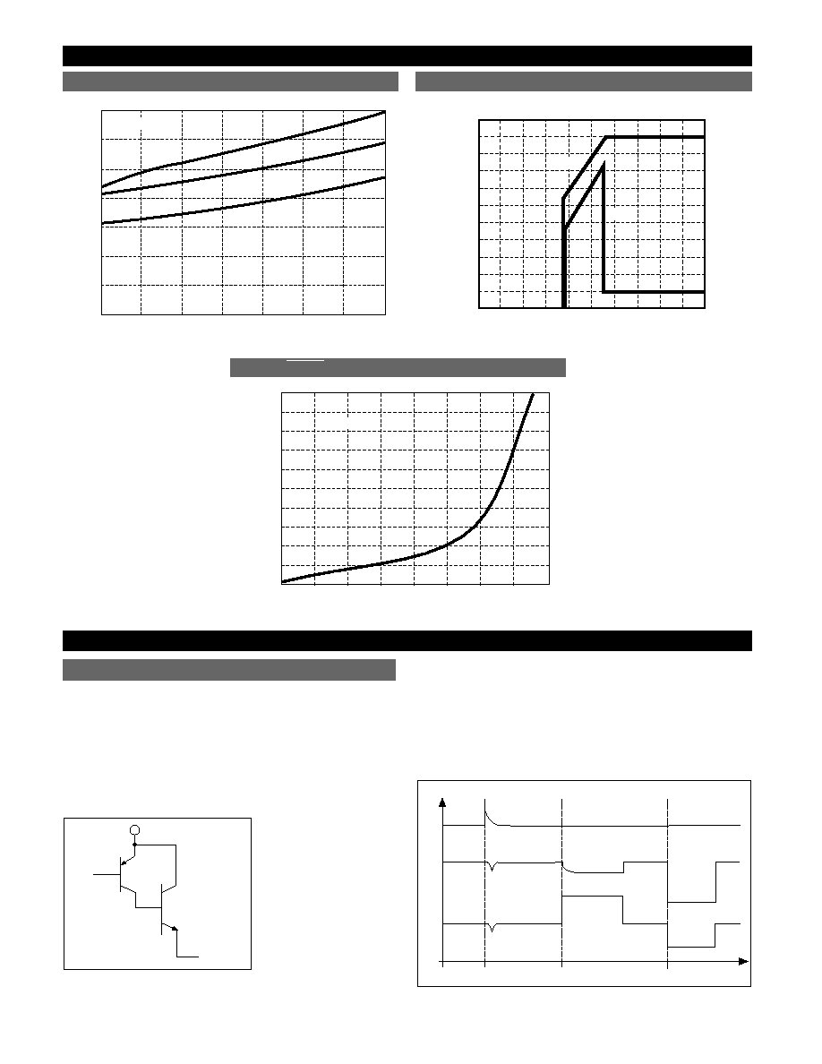
Output Stage
The composite PNP-
NPN output structure
(Figure 1) provides
300mA (typ) of output
current while maintain-
ing a low drop out volt-
age (1.00V, typ) and
drawing little quiescent
current (2.5mA).
The NPN pass device prevents deep saturation of the out-
put stage which in turn improves the IC’s efficiency by
preventing excess current from being used and dissipated
by the IC.
Output Stage Protection
The output stage is protected against overvoltage, short
circuit and thermal runaway conditions (Figure 2).
4
CS8120
Circuit Description
Typical Performance Characteristics: continued
Voltage Reference and Output Circuitry
V
OUT
V
IN
I
OUT
V
OUT
V
IN
Load
Dump
Short
Circuit
Thermal
Shutdown
> 30V
Figure 1: Composite Output Stage of the CS8120
5.5
10.0
0.0
Supply Voltage (V)
Supply Current (mA)
V
OUT
(V)
V
OUT
I
Q
5.0
4.0
3.0
2.0
1.0
0.0
22.0
20.0
16.0
12.0
8.0
4.0
0.0
2.0
4.0
6.0
8.0
Output Voltage and Supply Current vs. Input Voltage
2000
1800
1600
1400
1200
1000
800
600
400
200
0
1
5
10
15
20
25
30
35
40
V
IN
= 5V
Reset Output Current (mA)
Reset Output V
oltage (mV)
RESET Output Voltage vs. Output Current
3.5
3.0
2.5
2.0
1.5
1.0
0.5
0.0
0
50
-40
∞C
25
∞C
125
∞C
Output Current (mA)
Quiescent Current (mA)
V
IN
= 14V
100
150
200
250
300
350
Quiescent Current vs. Output Current Over Temperature
Figure 2: Typical Circuit Waveforms for Output Stage Protection.

If the input voltage rises above 26V (e.g. load dump), the
output shuts down. This response protects the internal cir-
cuitry and enables the IC to survive unexpected voltage
transients.
Using an emitter sense scheme, the amount of current
through the NPN pass transistor is monitored. Feedback
circuitry insures that the output current never exceeds a
preset limit.
Should the junction temperature of the power device
exceed 180˚C (typ) the power transistor is turned off.
Thermal shutdown is an effective means to prevent die
overheating since the power transistor is the principle heat
source in the IC.
The CS8120 contains two microprocessor compatible con-
trol functions:
and
(Figure 3).
Function
switches the output transistor. When the voltage
on the
lead exceeds 2.9V typ, the output pass
transistor turns off, leaving a high impedance facing the
load. The IC will remain in Sleep mode, drawing only
250µA, until the voltage on the lead drops below 2.1V typ.
Hysteresis (800mV) is built into the
function to
Figure 3: Circuit Waveforms for CS8120
provide good noise immunity.
Function
A
signal (low voltage) is generated as the IC pow-
ers up (V
OUT
> V
OUT
- 100mV) or when V
OUT
drops out of
regulation (V
OUT
< V
OUT
- 140mV, typ). 40mV of hysteresis
is included in the function to minimize oscillations.
The
output is an open collector NPN transistor,
controlled by a low voltage detection circuit. The circuit is
functionally independent of the rest of the IC, thereby
Figure 4: RC Network for
Delay circuitry
guaranteeing that the
signal is valid for V
OUT
as low
as 1V.
An external RC network on the
lead (Figure 4) pro-
vides a sufficiently long delay for most microprocessor
based applications. RC values can be chosen using the fol-
lowing formula:
R
TOT
¥ C
RST
where:
R
TOT
= R
RST
in parallel with R
IN,
R
IN
= µP port impedance,
C
RST
=
delay capacitor,
t
Delay
= desired delay time,
V
RST
= V
SAT
of lead
(0.7V @ turn - on), and
V
T
= µP logic threshold voltage.
RESET
RESET
]
[
RESET
RESET
RESET
C
RST
R
RST
C
2
22
mF
5V to
mP
and
System
Power
to
mP
RESET
Port
RESET
CS≠8120
V
OUT
RESET
RESET
RESET
(1) = NO RESET DELAY CAPACITOR
(2) = WITH RESET DELAY CAPACITOR
FOR 7V < V
IN
< 26V
V
OUT
V
RT(ON)
ENABLE
V
RT(OFF)
(1)
(2)
V
IN
V
IN(HI)
H
HI
LO
VR
PEAK
VR
SAT
VR
PEAK
RESET
ENABLE
ENABLE
ENABLE
ENABLE
RESET
ENABLE
Regulator Control Functions
5
–t
Delay
ln
)
V
T
– V
OUT
V
RST
– V
OUT
(
Applications Notes
CS8120
The circuit depicted in Figure 5 lets the microprocessor
control its power source, the CS8120 regulator. An I/O
port on the µP and the SWITCH port are used to drive the
base of Q1. When Q1 is driven into saturation, the voltage
on the
lead falls below its lower threshold. The
regulator’s output is switched out. When the drive cur-
rent is removed, the voltage on the
lead rises,
the output is switched off and the IC moves into Sleep
mode where it draws 250µA.
By coupling these two controls with
, the system
has added flexibility. Once the system is running, the
state of the SWITCH is irrelevant as long as the I/O port
continues to drive Q1. The µP can turn off its own power
by withdrawing drive current, once the SWITCH is open.
This software control at the I/O port allows the µP to fin-
ish key housekeeping functions before power is removed.
The logic options are summarized in Table 1 below
ENABLE
ENABLE
ENABLE
Circuit Description: continued
Table 1: Logic Control of CS8120 Output
µP I/O drive
SWITCH
Output
ON
Closed
LOW
ON
Open
LOW
ON
OFF
Closed
LOW
ON
Open
HIGH
OFF
ENABLE