The CS8121 is a 5V, 1A precision linear
regulator with two microprocessor
compatible control functions and pro-
tection circuitry included on chip. The
composite NPN-PNP output pass tran-
sistor assures a lower dropout voltage
(1.2V @ 1A) without requiring exces-
sive supply current (4mA).
The CS8121’s two logic control func-
tions make this regulator well suited to
applications requiring microprocessor-
based control at the board or module
level.
controls the output
stage. A high voltage (>2.9V) on
the
lead turns off the regula-
tor’s pass transistor and sends the IC
into Sleep mode where it draws only
250µA.
sends a
signal
when the IC is powering up or when-
ever the output voltage falls out of reg-
ulation. The
signal is valid
down to V
OUT
= 1V.
The CS8121 design optimizes supply
rejection by switching the internal
bandgap reference from the supply
input to the regulator output as soon as
the nominal output voltage is achieved.
Additional on chip filtering enhances
rejection of high frequency transients
on all external leads.
The CS8121 is fault protected against
short circuit, over voltage and thermal
runaway conditions.
RESET
RESET
RESET
ENABLE
ENABLE
1
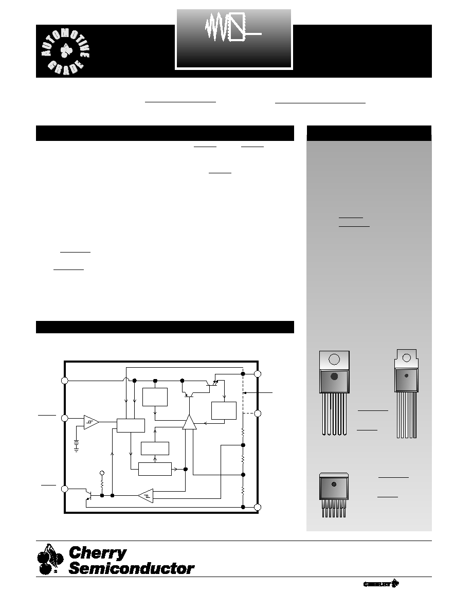
Features
Over
Voltage
Shutdown
RESET
Comparator
Error
Amplifier
+
-
TO V
OUT
+
+
-
VREF
ENABLE
Comparator
Bandgap
Supply
Output
Current
Limit
Bandgap
Reference
Thermal
Shutdown
-
V
IN
ENABLE
RESET
V
OUT
Gnd
V
OUT(SENSE)
5 Lead
TO-220
s
5V ± 4% Output Voltage
s
Low Dropout Voltage
(1.2V @ 1A)
s
Low Quiescent Current
(4mA @ I
OUT
= 1A)
s
µP Compatible Control
Functions
s
Low Current Sleep Mode
I
Q
= 250µA
s
Fault Protection
Thermal Shutdown
Short Circuit
60V Peak Transient
Voltage
ENABLE
RESET
Package Options
5 Lead TO-220
5 Lead TO-220
Overmolded
1
CS8121
5V, 1A Linear Regulator
with
and ENABLE
RESET
CS8121
Description
Block Diagram
1
1 V
IN
2
3 Gnd
4
5 V
OUT
RESET
ENABLE
7 Lead D
2
PAK
1
1 NC
2 V
IN
3
4 Gnd
5
6 V
OUT
7 V
OUT(SENSE)
RESET
ENABLE
Cherry Semiconductor Corporation
2000 South County Trail, East Greenwich, RI 02818
Tel: (401)885-3600 Fax: (401)885-5786
Email: info@cherry-semi.com
Web Site: www.cherry-semi.com
A Company
®
Rev. 5/4/99
2
Electrical Characteristics:
I
OUT
= 5mA, -40˚C ≤ T
J
≤150˚C , 7V ≤ V
IN
≤ 26V, -40°C ≤ T
A
≤ 125°C unless otherwise specified
PARAMETER
TEST CONDITIONS
MIN
TYP
MAX
UNIT
CS8121
Absolute Maximum Ratings
DC Input Voltage ...........................................................................................................................................................-0.7 to 26V
Peak Transient Voltage (46V Load Dump).............................................................................................................................60V
Output Current .................................................................................................................................................Internally Limited
Electrostatic Discharge (Human Body Model) ......................................................................................................................2kV
Operating, Temperature ..........................................................................................................................................-40C to 125°C
Junction Temperature...............................................................................................................................................-40C to 150°C
Storage Temperatures.............................................................................................................................................-55°C to 150°C
Lead Temperature Soldering
Wave Solder (through hole styles only) .....................................................................................10 sec. max, 260°C peak
Reflow (SMD styles only) ......................................................................................60 sec. max above 183°C, 230°C peak
s Output Stage
Output Voltage, V
OUT
7V ≤ V
IN
≤ 26V, 1mA ≤ I
OUT
≤ 1A
4.8
5.0
5.2
V
Line Regulation
7V ≤ V
IN
≤ 26V, I
OUT
= 5mA
0
50
mV
Load Regulation
5mA ≤ I
OUT
≤ 1A
10
70
mV
Supply Voltage Rejection
V
IN
= 14V
DC
+ 1V
RMS
54
70
dB
@120Hz, I
LOAD
= 50Ω
Dropout Voltage
I
OUT
= 1A
1.2
1.8
V
Quiescent Current
= High, V
IN
= 12V
0.25
0.65
mA
= Low, I
OUT
= 1A
4
20
mA
s Protection Circuits
Short Circuit Current
1.5
A
Thermal Shutdown
150
190
˚C
Overvoltage Shutdown
26
40
V
s
Saturation Voltage
1V < V
OUT
< V
RT(OFF),
3.1kΩ pull-up
0.1
0.4
V
to V
OUT
Output Leakage
= Low
0
25
µA
Current
V
OUT
> V
RT(ON)
, V
= V
OUT
Power ON/OFF
3.1kΩ pull-up to V
OUT
0.7
1.0
V
Peak Output Voltage
Threshold ON
V
OUT
- 0.10
V
OUT
- 0.04
V
(V
OUT
Increasing)
Threshold OFF
4.75
V
OUT
- 0.14
V
(V
OUT
Decreasing)
Threshold Hysteresis
10
40
mV
s
Input High Voltage
7V < V
IN
< 26V
2.9
3.9
V
Input Low Voltage
7V < V
IN
< 26V
1.1
2.1
V
Input Hysteresis
7V < V
IN
< 26V
0.4
0.8
2.8
V
Input Current
Gnd < V
IN(HI)
< V
OUT
0
±10
µA
ENABLE
RESET
RESET
RESET
RESET
RESET
ENABLE
RESET
RESET
RESET
ENABLE
ENABLE
3
CS8121
Package Lead Description
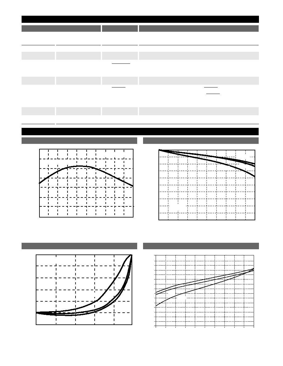
Typical Performance Characteristics
PACKAGE LEAD #
LEAD SYMBOL
FUNCTION
Junction Temperature
(˚C)
-40
-20
0
20
40
60
80
100
120 140 150
5.02
5.01
5
4.99
4.98
4.97
4.96
4.95
I
OUT
= 100mA
V
OUT
(V)
5.00V @ 25˚C
Output Voltage vs. Temperature
-35
-40
-45
-50
0
200
400
600
800
1A
-30
-25
-20
-15
-10
-5
0
– 4 0
∞ C
2 5 ∞ C
1 2 5
∞ C
I
OUT
(A)
Load Reg. (mV)
V
IN
=14V
Load Regulation vs. Output Current Over Temperature
Line Reg. (mV)
V
IN
= 7 to 26V
-40˚C
125˚C
25˚C
50
40
30
20
10
0
-10
I
OUT
(A)
0
0.2
0.4
0.6
0.8
1A
Line Regulation vs. Output Current Over Temperature
1.5
1.4
1.3
1.2
1.1
1.0
0.9
0.8
0.7
0.6
0.5
0.4
0.3
0.2
0.1
0.0
0
0.2
0.6
0.9
1.0
0.1
0.3
0.5
0.4
0.7
0.8
I
OUT
(A)
Dropout V
oltage (V)
-40
∞C
25
∞C
125
∞C
Dropout Voltage vs. Output Current Over Temperature
7 Lead
5 Lead TO-220 &
D
2
PAK
Overmolded TO-220
1
NC
No Connection.
2
1
V
IN
Supply voltage to IC, usually direct from the battery.
3
2
CMOS compatible logical. V
OUT
is disabled i.e. placed in a
high impedance state when ENABLE is high.
4
3
Gnd
Ground connection.
5
4
CMOS compatible output lead.
goes low whenever
V
OUT
falls out of regulation. The
delay is externally
programmed.
6
5
V
OUT
Regulated output voltage, 5V (typ).
7
V
OUT(SENSE)
Remote sensing of output voltage.
RESET
RESET
RESET
ENABLE
4
CS8121
Typical Performance Characteristics: continued
Precision Voltage Reference
The regulated output voltage depends on the precision
band gap voltage reference in the IC. By adding an error
amplifier into the feedback loop, the output voltage is
maintained within ±4% over temperature and supply vari-
ation.
Output Stage
The composite PNP-
NPN output structure
(Figure 1) provides 1A
(typ) of output current
while maintaining a
low drop out voltage
(1.2V) and drawing lit-
tle quiescent current
(4mA).
The NPN pass device prevents deep saturation of the output
stage which in turn improves the IC’s efficiency by prevent-
ing excess current from being used and dissipated by the IC.
Output Stage Protection
The output stage is protected against overvoltage, short
circuit and thermal runaway conditions (Figure 2).
Voltage Reference and Output Circuitry
V
OUT
V
IN
I
OUT
V
OUT
V
IN
Load
Dump
Short
Circuit
Thermal
Shutdown
> 30V
Figure 1. Composite Output Stage of the CS8121
Circuit Description
3.5
3.0
2.5
2.0
1.5
1.0
0.5
0.0
0
0.1
-40
∞C
25
∞C
125
∞C
VIN = 14V
0.2
0.3
0.4
0.5
0.6
0.7
0.8
0.9
I
OUT
Quiescent Current (mA)
1.0
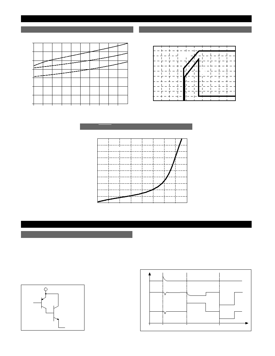
Quiescent Current vs. Output Current Over Temperature
22.0
20.0
16.0
12.0
8.0
4.0
0.0
10.0
8.0
6.0
4.0
2.0
0.0
0.0
1.0
2.0
3.0
4.0
5.0
5.5
Supply Voltage
Supply Current (mA)
V
OUT
(V)
V
OUT
I
Q
Output Voltage and Supply Current vs. Input Voltage
2000
1800
1600
1400
1200
1000
800
600
400
200
0
1
5
10
15
20
25
30
35
40
V
IN
= 5V
Reset Output Current (mA)
Reset Output V
oltage (mV)
RESET Output Voltage vs. Output Current
Figure 2. Typical Circuit Waveforms for Output Stage Protection.
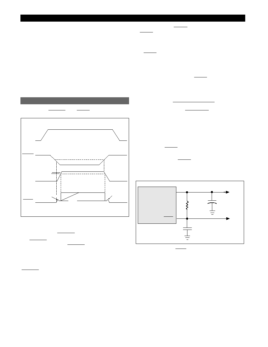
If the input voltage rises above 30V (e.g. load dump), the
output shuts down. This response protects the internal cir-
cuitry and enables the IC to survive unexpected voltage
transients.
Using an emitter sense scheme, the amount of current
through the NPN pass transistor is monitored. Feedback
circuitry insures that the output current never exceeds a
preset limit.
Should the junction temperature of the power device
exceed 180˚C (typ) the power transistor is turned off.
Thermal shutdown is an effective means to prevent die
overheating since the power transistor is the principle
heat source in the IC.
The CS8121 contains two microprocessor compatible con-
trol functions:
and
(Figure 3).
Function
The
function switches the output transistor.
When the voltage on the
lead exceeds 2.9V typ,
the output pass transistor turns off, leaving a high
impedance facing the load. The IC will remain in Sleep
mode, drawing only 250µA, until the voltage on the lead
drops below 2.1V typ. Hysteresis (800mV) is built into the
function to provide good noise immunity.
Function
A
signal (low voltage) is generated as the IC pow-
ers up (V
OUT
> V
OUT
- 100mV) or when V
OUT
drops out of
regulation (V
OUT
< V
OUT
- 140mV, typ). 40mV of hysteresis
is included in the function to minimize oscillations.
The
output is an open collector NPN transistor,
controlled by a low voltage detection circuit. The circuit is
functionally independent of the rest of the IC, thereby
guaranteeing that the RESET signal is valid for V
OUT
as
low as 1V.
An external RC network on the
lead (Figure 4) pro-
vides a sufficiently long delay for most microprocessor
based applications. RC values can be chosen using the
following formula:
R
TOT
¥
C
RST
where:
R
TOT
= R
RST
in parallel with R
IN
,
R
IN
= µP port impedance,
C
RST
=
delay capacitor,
t
Delay
= desired delay time,
V
RST
= V
SAT
of
lead (0.7V @ turn - on), and
V
T
= µP logic threshold voltage.
RESET
RESET
]
[
RESET
RESET
RESET
RESET
ENABLE
ENABLE
ENABLE
ENABLE
RESET
ENABLE
5
Regulator Control Functions
Figure 4. RC Network for
Delay
RESET
CS8121
Circuit Description: continued
–t
Delay
ln
)
V
T
– V
OUT
V
RST
– V
OUT
(
RESET
CS8121
V
OUT
C
RST
R
RST
10
mF
tantalum
5V to
mP
and
System
Power
to
mP
RESET
Port
(1) = NO RESET DELAY CAPACITOR
(2) = WITH RESET DELAY CAPACITOR
FOR 7V < V
IN
< 26V
V
OUT
V
RT(ON)
ENABLE
V
RT(OFF)
(1)
(2)
V
IN
V
IN(HI)
HI
LO
VR
PEAK
VR
SAT
VR
PEAK
RESET
Figure 3. Circuit Waveforms for the CS8121
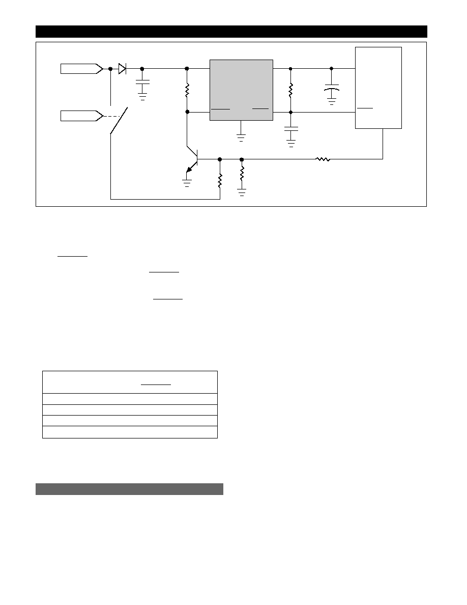
The circuit depicted in Figure 5 lets the microprocessor
control its power source, the CS8121 regulator. An I/O
port on the µP and the SWITCH port are used to drive the
base of Q1. When Q1 is driven into saturation, the voltage
on the
lead falls below its lower threshold and
the regulator’s output is switched on. When the drive cur-
rent is removed, the voltage on the
lead rises,
the output is switched off and the IC moves into Sleep
mode where it typically draws 250µA.
By coupling these two controls with
, the system
has added flexibility. Once the system is running, the
state of the SWITCH is irrelevant as long as the I/O port
continues to drive Q1. The µP can turn off its own power
by withdrawing drive current, once the SWITCH is open.
This software control at the I/O port allows the µP to fin-
ish key housekeeping functions before power is removed.
The logic options are summarized in Table 1 below
The I/O port of the µP typically provides 50 µA to Q1. In
automotive applications the SWITCH is connected to the
ignition switch.
The output or compensation capacitor C
2
helps determine
three main characteristics of a linear regulator: start-up
delay, load transient response and loop stability.
The capacitor value and type should be based on cost,
availability, size and temperature constraints. A tantalum
or aluminum electrolytic capacitor is best, since a film or
ceramic capacitor with almost zero ESR can cause insta-
bility. The aluminum electrolytic capacitor is the least
expensive solution, but, if the circuit operates at low
temperatures (-25°C to -40°C), both the value and ESR of
the capacitor will vary considerably. The capacitor manu-
facturers data sheet usually provides this information.
The value for the output capacitor C
2
shown in the test
and applications circuit should work for most applica-
tions, however it is not necessarily the optimized solu-
tion.
To determine an acceptable value for C
2
for a particular
application, start with a tantalum capacitor of the recom-
mended value and work towards a less expensive alterna-
tive part.
Step 1:
Place the completed circuit with a tantalum
capacitor of the recommended value in an environmental
chamber at the lowest specified operating temperature
and monitor the outputs with an oscilloscope. A decade
box connected in series with the capacitor will simulate
the higher ESR of an aluminum capacitor. Leave the
decade box outside the chamber, the small resistance
added by the longer leads is negligible.
Step 2:
With the input voltage at its maximum value,
increase the load current slowly from zero to full load
while observing the output for any oscillations. If no
oscillations are observed, the capacitor is large enough to
ensure a stable design under steady state conditions.
Step 3:
Increase the ESR of the capacitor from zero using
the decade box and vary the load current until oscillations
appear. Record the values of load current and ESR that
cause the greatest oscillation. This represents the worst
case load conditions for the regulator at low temperature.
Step 4
: Maintain the worst case load conditions set in
step 3 and vary the input voltage until the oscillations
increase. This point represents the worst case input volt-
age conditions.
Step 5:
If the capacitor is adequate, repeat steps 3 and 4
with the next smaller valued capacitor. A smaller capaci-
tor will usually cost less and occupy less board space. If
the output oscillates within the range of expected operat-
ing conditions, repeat steps 3 and 4 with the next larger
standard capacitor value.
ENABLE
ENABLE
ENABLE
6
Stability Considerations
CS8121
C
1
0.1
mF
V
IN
Gnd
RESET
CS≠8121
V
OUT
ENABLE
500k
W
Q
1
500k
W
100k
W
100k
W
C
RST
R
RST
C
2
10
mF
V
CC
I/O Port
mP
V
BAT
RESET
SWITCH
Applications Notes
Figure 5. Microprocessor control of CS8121 using external switching transistor Q
1
.
Table 1: Logic Control of CS8121 Output
µP I/O drive
SWITCH
Output
ON
Closed
LOW
ON
Open
LOW
ON
OFF
Closed
LOW
ON
Open
HIGH
OFF
ENABLE
Step 6:
Test the load transient response by switching in
various loads at several frequencies to simulate its real
working environment. Vary the ESR to reduce ringing.
Step 7:
Remove the unit from the environmental chamber
and heat the IC with a heat gun. Vary the load current as
instructed in step 5 to test for any oscillations.
Once the minimum capacitor value with the maximum
ESR is found, a safety factor should be added to allow for
the tolerance of the capacitor and any variations in regula-
tor performance. Most good quality aluminum electrolytic
capacitors have a tolerance of +/- 20% so the minimum
value found should be increased by at least 50% to allow
for this tolerance plus the variation which will occur at
low temperatures. The ESR of the capacitor should be less
than 50% of the maximum allowable ESR found in step 3
above.
The maximum power dissipation for a single output regu-
lator (Figure 7) is:
P
D(max)
= {V
IN(max)
- V
OUT(min)
}I
OUT(max)
+ V
IN(max)
I
Q
(1)
where:
V
IN(max)
is the maximum input voltage,
V
OUT(min)
is the minimum output voltage,
I
OUT(max)
is the maximum output current for the applica-
tion, and
I
Q
is the quiescent current the regulator consumes at
I
OUT(max)
.
Once the value of P
D(max)
is known, the maximum permis-
sible value of R
QJA
can be calculated:
R
QJA
=
(2)
The value of R
QJA
can then be compared with those in
the package section of the data sheet. Those packages
with R
QJA
's less than the calculated value in equation 2
will keep the die temperature below 150°C.
In some cases, none of the packages will be sufficient to
dissipate the heat generated by the IC, and an external
heatsink will be required.
A heat sink effectively increases the surface area of the
package to improve the flow of heat away from the IC
and into the surrounding air.
Each material in the heat flow path between the IC and
the outside environment will have a thermal resistance.
Like series electrical resistances, these resistances are
summed to determine the value of R
QJA
:
R
QJA
= R
QJC
+ R
QCS
+ R
QSA
(3)
where:
R
QJC
= the junction–to–case thermal resistance,
R
QCS
= the case–to–heatsink thermal resistance, and
R
QSA
= the heatsink–to–ambient thermal resistance.
R
QJC
appears in the package section of the data sheet. Like
R
QJA
, it too is a function of package type. R
QCS
and R
QSA
are functions of the package type, heatsink and the inter-
face between them. These values appear in heat sink data
sheets of heat sink manufacturers.
150°C - T
A
P
D
7
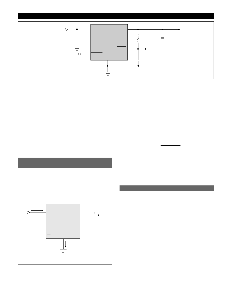
Application Notes: continued
Calculating Power Dissipation
in a Single Output Linear Regulator
V
IN
Smart
Regulator
V
OUT
I
OUT
I
IN
I
Q
Control
Features
}
Figure 7: Single output regulator with key performance parameters
labeled.
CS8121
RESET
V
OUT
R
RST
C
2
**
10
mF
C
RST
ENABLE
V
IN
C
1
*
0.1
mF
to
mP
RESET
Port
5V to
mP and
System
Power
CS-8121
C
1
*required if regulator is located far from
the power supply filter.
C
2
** required for stability.
Heat Sinks
Figure 6: Test and application circuit showing output compensation.
Part Number
Description
CS8121YT5
5 Lead TO-220 Straight
CS8121YTVA5
5 Lead TO-220 Vertical
CS8121YTHA5
5 Lead TO-220 Horizontal
CS8121YTFVA5
5 Lead Overmolded TO-220
Vertical
CS8121YDPS7
7 Lead D
2
PAK Short-Leaded
CS8121YDPSR7
7 Lead D
2
PAK Short-Leaded
(tape & reel)
8
Ordering Information
Rev. 5/4/99
Cherry Semiconductor Corporation reserves the right to
make changes to the specifications without notice. Please
contact Cherry Semiconductor Corporation for the latest
available information.
Thermal Data
5 Lead
5 Lead
7 Lead
TO-220 TO-220
D
2
PAK
(Overmold)
R
QJC
typ
4.0
2.5
2.5
˚C/W
R
QJA
typ
50
50
10-50* ˚C/W
*Depending on thermal properties of substrate, R
QJA
= R
QJC
+ R
QCA.
Package Specification
PACKAGE THERMAL DATA
PACKAGE DIMENSIONS IN mm (INCHES)
CS8121
© 1999 Cherry Semiconductor Corporation
5 Lead TO-220 (T) Straight
2.87 (.113)
2.62 (.103)
6.93(.273)
6.68(.263)
9.78 (.385)
10.54 (.415)
1.02(.040)
0.63(.025)
1.83(.072)
1.57(.062)
0.56 (.022)
0.36 (.014)
2.92 (.115)
2.29 (.090)
1.40 (.055)
1.14 (.045)
4.83 (.190)
4.06 (.160)
6.55 (.258)
5.94 (.234)
14.22 (.560)
13.72 (.540)
1.02 (.040)
0.76 (.030)
3.71 (.146)
3.96 (.156)
14.99 (.590)
14.22 (.560)
5 Lead TO-220 (TVA) Vertical
1.68
(.066) typ
1.70 (.067)
7.51 (.296)
1.78 (.070)
4.34 (.171)
0.56 (.022)
0.36 (.014)
1.40 (.055)
1.14 (.045)
4.83 (.190)
4.06 (.160)
14.99 (.590)
14.22 (.560)
2.92 (.115)
2.29 (.090)
.94 (.037)
.69 (.027)
8.64 (.340)
7.87 (.310)
6.80 (.268)
10.54 (.415)
9.78 (.385)
2.87 (.113)
2.62 (.103)
6.55 (.258)
5.94 (.234)
3.96 (.156)
3.71 (.146)
5 Lead Overmolded TO-220 (TFVA) Vertical
10.3 (.405)
10.0 (.395)
.761 (.030)
.508 (.020)
15.6 (.614)
15.3 (.604)
3.17 (.125)
2.92 (.115)
7.18 (.283)
6.94 (.273)
3.30 (.130)
2.89 (.114)
10.4 (.409)
.94 (.037)
.69 (.027)
1.70 (.067)
6.80 (.268)
1.68 (.066) TYP
3.30 (.130)
3.05 (.120)
DIA
2.79 (.110)
2.54 (.100)
4.70 (.185)
4.44 (.175)
5.89 (.232)
3.10 (.122)
.56 (.022)
.36 (.014)
4.01
(.158)
8.05 (.317)
Note:
Leads maintain
a right angle
with respect to
the package
body to within
± .015≤.
3.18 (.125)
2.92 (.115)
7 Lead D
2
PAK (DPS)* Short-Leaded
1.98 (.078)
1.47 (.058)
14.71 (.579)
13.69 (.539)
4.57 (.180)
4.31 (.170)
1.40 (.055)
1.14 (.045)
2.79 (.110)
2.54 (.100)
TERMINAL 8
7.75 (.305)
REF
6.50 (.256) REF
10.31 (.406)
10.05 (.396)
1.27 (.050)
REF
1.68 (.066)
1.40 (.055)
.254 (.010)
REF
0.91 (.036)
0.66 (.026)
8.53 (.336)
8.28 (.326)
0.10 (.004)
0.00 (.000)
*CHERRY SEMICONDUCTOR SHORT-LEADED FOOTPRINT