The CS8122 is a precision 5V linear reg-
ulator capable of sourcing in excess of
750mA. The
’s delay time is
externally programmed using a discrete
RC network. During power up, or when
the output goes out of regulation, the
lead remains in the low state
for the duration of the delay. This func-
tion is independent of the input voltage
and will function correctly as long as
the output voltage remains at or above
1V. Hysteresis is included in the Delay
and the
comparators to
improve noise immunity. A latching
discharge circuit is used to discharge
the delay capacitor when it is triggered
by a brief fault condition.
The regulator is protected against a
variety of fault conditions: i.e. reverse
battery, overvoltage, short circuit and
thermal runaway conditions. The regu-
lator is protected against voltage tran-
sients ranging from -50V to +40V. Short
circuit current is limited to 1.2A (typ).
The CS8122 is an improved replacement
for the CS8126 and features a tighter tol-
erance on its output voltage (2% vs 4%).
The CS8122 is packaged in a 5 lead
TO–220 with copper tab. The copper tab
can be connected to a heat sink if
necessary.
RESET
RESET
RESET
1
2% 5V, 750mA Low Dropout Linear
Regulator with Delayed RESET
Features
s
5V +/- 2% Regulated
Output
s
Low Dropout Voltage
(0.6V @ 0.5A)
s
750mA Output Current
Capability
s
Externally Programmed
Delay
s
Fault Protection
Reverse Battery
60V Load Dump
-50V Reverse Transient
Short Circuit
Thermal Shutdown
RESET
Package Options
5 Lead TO-220
CS8122
Description
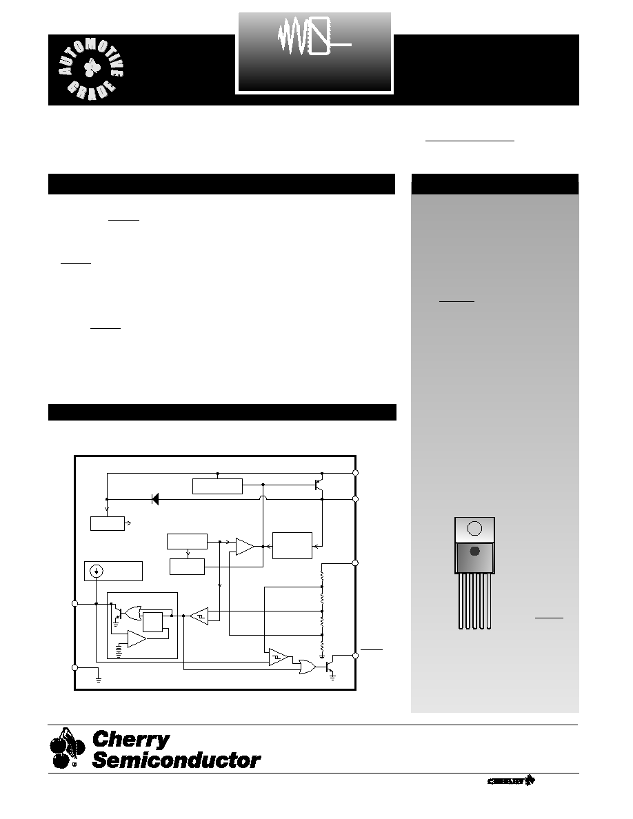
Block Diagram
V
OUT
V
IN
Over Voltage
Shutdown
Pre-
Regulator
Regulated Supply
for Circuit Bias
Bandgap
Reference
Thermal
Shutdown
Anti-Saturation
and
Current Limit
-
+
+
-
Q
R
S
VDISC
+
-
+
-
Delay
Gnd
RESET
V
OUT
SENSE
Error Amplifier
Latching Discharge
Delay Comparator
Charge
Current
Generator
CS8122
1 V
IN
2 V
OUT
3 Gnd
4 Delay
5 RESET
1
A Company
®
Rev. 2/5/99
Cherry Semiconductor Corporation
2000 South County Trail, East Greenwich, RI 02818
Tel: (401)885-3600 Fax: (401)885-5786
Email: info@cherry-semi.com
Web Site: www.cherry-semi.com

2
Electrical Characteristics: -40˚C ≤ T
A
≤ +125˚C, -40˚C ≤ T
J
≤ +150˚C, 6V ≤ V
IN
≤ 26V, 5mA ≤ I
OUT
≤ 500mA,
R
= 4.7kΩ to V
CC
unless otherwise noted*
RESET
PARAMETER
TEST CONDITIONS
MIN
TYP
MAX
UNIT
Absolute Maximum Ratings
Input Operating Range..................................................................................................................................................-0.5 to 26V
Power Dissipation.............................................................................................................................................Internally Limited
Transient Input Voltage .................................................................................................................................................-50V, 60V
Output Current .................................................................................................................................................Internally Limited
ESD Susceptibility (Human Body Model)..............................................................................................................................4kV
Junction Temperature .............................................................................................................................................-55°C to 150°C
Storage Temperature...............................................................................................................................................-55°C to 150°C
Lead Temperature Soldering
Wave Solder (through hole styles only) .....................................................................................10 sec. max, 260°C peak
CS8122
* To observe safe operating junction temperatures, low duty cycle pulse testing is used in tests where applicable.
Delay Time =
C
Delay
x V
Delay Threshold Charge
= C
Delay
x 3.5 x 10
5
(typ)
I
Charge
s
Output Stage (V
OUT
)
Output Voltage
4.9
5.0
5.1
V
Dropout Voltage
I
OUT
= 500mA
0.35
0.60
V
Supply Current
I
OUT
≤ 10mA
2
7
mA
I
OUT
≤ 100mA
6
12
I
OUT
≤ 500mA
55
100
Line Regulation
6V ≤ V
IN
≤ 26V, I
OUT
= 50mA
5
50
mV
Load Regulation
50mA ≤ I
OUT
≤ 500mA, V
IN
= 14V
10
50
mV
Ripple Rejection
f = 120Hz, V
IN
= 7 to 17V,
54
75
dB
I
OUT
= 250mA
Current Limit
0.75
1.20
A
Overvoltage Shutdown
32
40
V
Maximum Line Transient
V
OUT
≤ 5.5V
60
95
V
Reverse Polarity Input
V
OUT
≥ -0.6V, 10Ω Load
-15
-30
V
Voltage DC
Reverse Polarity Input
1% Duty Cycle, T < 100ms,
-50
-80
V
Voltage Transient
10Ω Load
Thermal Shutdown
Guaranteed by Design
150
180
210
°C
s
and Delay Functions
Delay Charge Current
V
DELAY
= 2V
5
10
15
µA
Threshold
V
OUT
Increasing, V
RT(ON)
4.65
4.90
V
OUT
-0.01
V
V
OUT
Decreasing, V
RT(OFF)
4.50
4.70
V
OUT
-0.16
V
Hysteresis
V
RH
= V
RT(ON)
- V
RT(OFF)
150
200
250
mV
Delay Threshold
Charge, V
DC(HI)
3.25
3.50
3.75
V
Discharge, V
DC(L)
2.85
3.10
3.35
V
Delay Hysteresis
200
400
800
mV
Output Voltage Low
1V < V
OUT
< V
RT(L)
, 3kΩ to V
OUT
0.1
0.4
V
Output Leakage
V
OUT
> V
RT(H)
0
10
µA
Current
Delay Capacitor
Discharge Latched “ON”,
0.2
0.5
V
Discharge Voltage
V
OUT
> V
RT
Delay Time
C
DELAY
= 0.1µF
16
32
48
ms
RESET
RESET
RESET
RESET
RESET
3
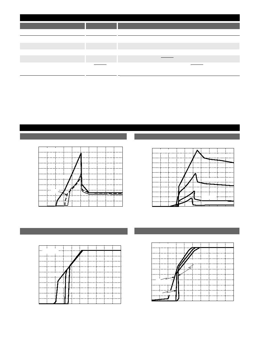
Typical Performance Characteristics
0.0
0.0
Quiescent Current
(mA)
V
IN
(V)
1.0
2.0
3.0
4.0
5.0
6.0
7.0
8.0
9.0
10.0
5.0
10.0
15.0
20.0
25.0
30.0
35.0
40.0
45.0
50.0
55.0
125˚C
25˚C
-40˚C
R
load
= 25
W
0.0
0.0
Quiescent Current
(mA)
V
IN
(V)
1.0
2.0
3.0
4.0
5.0
6.0
7.0
8.0
9.0
10.0
20.0
40.0
60.0
80.0
100.0
120.0
R
load
= 6.67
W
R
load
= 10
W
R
load
= 25
W
R
load
= NO LOAD
Room Temp.
0.0
0.0
V
OUT
(V)
V
IN
(V)
1.0
2.0
3.0
4.0
5.0
6.0
7.0
8.0
9.0
10.0
0.5
1.0
1.5
2.0
2.5
3.0
3.5
4.0
4.5
5.0
5.5
R
load
= 25
W
125˚C
25˚C
-40˚C
Output Voltage vs Input Voltage over Temperature
Quiescent Current vs Input Voltage over Load Resistance
Quiescent Current vs Input Voltage over Temperature
0.0
0.0
V
OUT
(V)
V
IN
(V)
1.0
2.0
3.0
4.0
5.0
6.0
7.0
8.0
9.0
10.0
0.5
1.0
1.5
2.0
2.5
3.0
3.5
4.0
4.5
5.0
5.5
R
load
=
NO LOAD
R
load
= 6.67
W
R
load
= 10
W
Room Temp.
V
OUT
vs. V
IN
over R
LOAD
Package Lead Description
PACKAGE LEAD #
LEAD SYMBOL
FUNCTION
CS8122
R
load
=25Ω
5Lead TO-220
1
V
IN
Unregulated supply voltage to IC.
2
V
OUT
Regulated 5V output.
3
Gnd
Ground connection.
4
Delay
Timing capacitor for
function.
5
CMOS/TTL compatible output lead.
goes low whenev-
er V
OUT
drops below 6% of it's regulated value.
RESET
RESET
RESET
4
0
0
DROPOUT
VOL
T
AGE (mV)
OUTPUT CURRENT (mA)
100
200
300
400
500
600
700
800
100
200
300
400
500
600
700
800
900
25˚C
-40˚C
125˚C
0
0
QUIESCENT
CURRENT
(mA)
OUTPUT CURRENT (mA)
10
20
30
40
50
60
70
80
90
100
100
200
300
400
500
600
700
800
V
IN
= 14V
125˚C
25˚C
-40˚C
0
10
0
REJECTION (dB)
FREQUENCY (Hz)
10
1
10
2
10
3
10
4
10
5
10
6
10
7
10
8
10
20
30
40
50
60
70
80
90
I
OUT
= 250mA
C
OUT
= 10
mF, ESR = 10W
C
OUT
= 10
mF, ESR = 1W
C
OUT
= 10
mF, ESR = 1 & 0.1mF,
ESR = 0
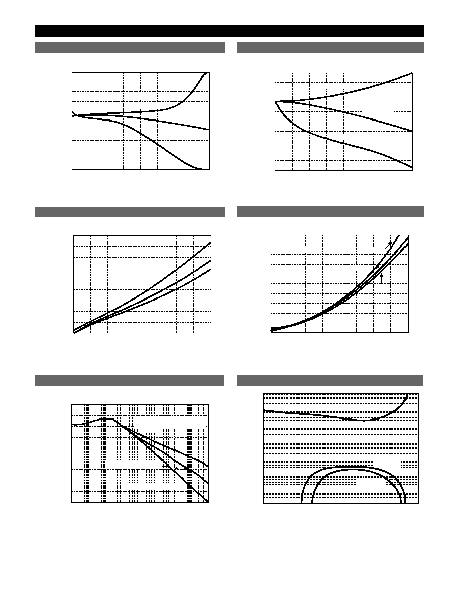
Ripple Rejection
Quiescent Current vs. Output Current
Dropout Voltage vs. Output Current
Typical Performance Characteristics: continued
-100
0
LINE REGULA
TION (mV)
OUTPUT CURRENT (mA)
-80
-60
-40
-20
0
20
40
60
80
100
100
200
300
400
500
600
700
800
V
IN
6-26V
TEMP = 25˚C
TEMP = - 40˚C
TEMP = 125˚C
-14
0
LOAD REGULA
TION (mV)
OUTPUT CURRENT (mA)
-12
-10
-8
-6
-4
-2
0
2
4
6
100
200
300
400
500
600
700
800
TEMP = 25˚C
TEMP = 125˚C
V
IN
= 14V
TEMP = -40˚C
Load Regulation vs. Output Current
Line Regulation vs. Output Current
10
0
ESR (ohms)
Output Current (mA)
10
1
10
2
10
3
10
1
10
2
10
3
10
-4
10
0
10
-1
10
-2
10
-3
C
O
= 68
mF
C
O
= 47
mF
C
O
= 47/68
mF
Stable Region
Output Capacitor ESR
CS8122
The CS8122
function, has hysteresis on both the
reset and delay comparators, a latching Delay capacitor
discharge circuit, and operates down to 1V.
The
circuit output is an open collector type with
ON and OFF parameters as specified. The
output
NPN transistor is controlled by the two circuits described
(see Block Diagram).
The Low Voltage Inhibit Circuit monitors output voltage,
and when output voltage is below the specified minimum,
causes the
output transistor to be in the ON (satu-
ration) state. When the output voltage is above the speci-
fied level, this circuit permits the
output transistor
to go into the OFF state if allowed by the
Delay cir-
cuit.
The Reset Delay Circuit provides a programmable (by
external capacitor) delay on the
output lead. The
Delay lead provides source current to the external delay
capacitor only when the Low Voltage Inhibit circuit indi-
cates that output voltage is above V
RT(ON)
. Otherwise, the
Delay lead sinks current to ground (used to discharge the
delay capacitor). The discharge current is latched ON
when the output voltage is below V
RT(OFF)
. The Delay
capacitor is fully discharged anytime the output voltage
falls out of regulation, even for a short period of time. This
feature ensures that a controlled
pulse is generated
following detection of an error condition. The circuit
allows the
output transistor to go to the OFF (open)
state only when the voltage on the Delay lead is higher
than V
DC(HI)
.
RESET
RESET
RESET
Reset Delay Circuit
RESET
RESET
RESET
Low Voltage Inhibit Circuit
RESET
RESET
RESET
5
V
RH
V
OUT
V
RT(ON)
V
RT(OFF)
V
RL
Delay
V
DC(HI)
V
DC(LO)
V
DH
t
Delay
V
DIS
(3)
(1)
(2)
(2)
RESET
(1) = No Delay Capacitor
(2) = With Delay Capacitor
(3) = Max: RESET Voltage (1.0V)
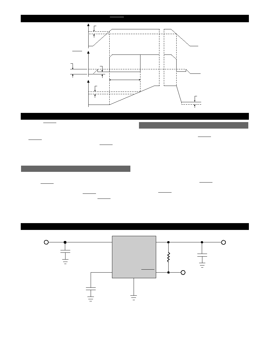
RESET Circuit Waveform
Circuit Description
Test Circuit
C
IN
*
100nF
V
IN
Delay
Gnd
RESET
V
OUT
CS8122
C
OUT
**
10
mF
R
RST
4.7k
W
C
Delay
0.1
mF
CS8122
*C
IN
required if regulator is far from power source filter.
**C
OUT
required for stability.