1
s
Low Dropout Voltage
(0.6V at 0.5A)
s
3% Output Accuracy
s
Active
s
External
Delay
for Reset
s
Protection Circuitry
Reverse Battery
Protection
+60V, -50V Peak
Transient Voltage
Short Circuit Protection
Internal Thermal
Overload Protection
RESET
RESET
Features
Package Options
5 L TO-220
7 L D
2
PAK
Tab (Gnd)
Tab (Gnd)
1
CS8126, -1, -2
5V, 750mA Low Dropout Linear Regulator
with Delayed RESET
CS8126,-1,-2
Description
The CS8126 is a low dropout, high cur-
rent 5V linear regulator. It is an
improved replacement for the CS8156.
Improvements include higher accuracy,
tighter saturation control, better supply
rejection, and enhanced
circuit-
ry. Familiar PNP regulator features
such as reverse battery protection, over-
voltage shutdown, thermal shutdown,
and current limit make the CS8126 suit-
able for use in automotive and battery
operated equipment. Additional on-
chip filtering has been included to
enhance rejection of high frequency
transients on all external leads.
An active microprocessor
func-
tion is included on-chip with externally
programmable delay time. During
power-up, or after detection of any
error in the regulated output,
the
lead will remain in the low
state for the duration of the delay.
Types of errors include short circuit,
low input voltage, overvoltage shut-
down, thermal shutdown, or others that
cause the output to become unregulat-
ed. This function is independent of the
input voltage and will function correct-
ly with an output voltage as low as 1V.
Hysteresis is included in both the reset
and Delay comparators for enhanced
noise immunity. A latching discharge
circuit is used to discharge the Delay
capacitor, even when triggered by a rel-
atively short fault condition. This circuit
improves upon the commonly used
SCR structure by providing full capaci-
tor discharge (0.2V type).
Note:The CS8126 is lead compatible
with the LM2925, TLE4260, L4947,
LM2927, and LM2926.
RESET
RESET
RESET
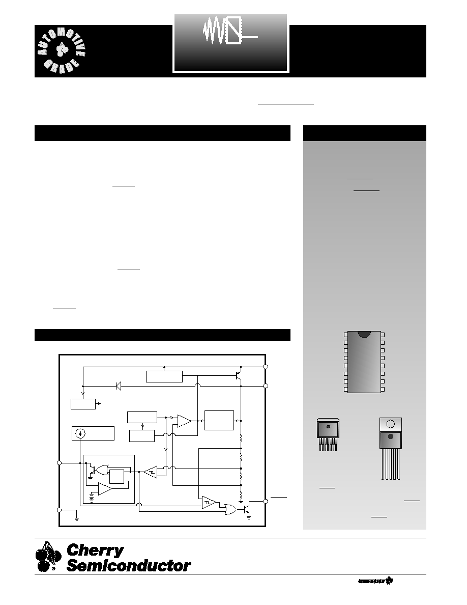
Block Diagram
V
OUT
V
IN
Over Voltage
Shutdown
Pre-
Regulator
Regulated Supply
for Circuit Bias
Bandgap
Reference
Thermal
Shutdown
Error
Amp
Anti-Saturation
and
Current Limit
Charge
Current
Generator
Latching
Discharge
Reset
Comparator
Delay
Comparator
-
+
+
-
Q
R
S
V
Discharge
+
-
+
-
Delay
Gnd
RESET
CS8126-1
1 V
IN
2 V
OUT
3 Gnd
4 Delay
5 RESET
CS8126-2
1 V
IN
2 RESET
3 Gnd
4 Delay
5 V
OUT
16 Lead SOIC Wide
1
V
IN
V
OUT
Delay
––––––
RESET
V
OUT(SENSE)
NC
NC
Gnd
NC
NC
NC
NC
NC
NC
NC
NC
A Company
®
Rev. 5/4/99
1
1 V
IN
2 V
OUT
3 V
OUT(SENSE)
4 Gnd
5 Delay
6 RESET
7 NC
Cherry Semiconductor Corporation
2000 South County Trail, East Greenwich, RI 02818
Tel: (401)885-3600 Fax: (401)885-5786
Email: info@cherry-semi.com
Web Site: www.cherry-semi.com
2
PARAMETER
TEST CONDITIONS
MIN
TYP
MAX
UNIT
Electrical Characteristics: T
A
= -40˚C to +125˚C, T
J
= -40˚C to +150˚C, V
IN
= 6 to 26V, I
O
=5 to 500mA,
R
RESET
= 4.7kΩ to V
CC,
unless otherwise noted.
Absolute Maximum Ratings
Power Dissipation.............................................................................................................................................Internally Limited
Peak Transient Voltage (46V Load Dump) .................................................................................................................-50V, 60V
Output Current .................................................................................................................................................Internally Limited
ESD Susceptibility (Human Body Model)..............................................................................................................................4kV
Junction Temperature .............................................................................................................................................-40°C to 150°C
Storage Temperature...............................................................................................................................................-55°C to 150°C
Lead Temperature Soldering Wave Solder (through hole styles only) ..........................................10 sec. max, 260°C peak
Reflow (SMD styles only) ..........................................60 sec. max above 183°C, 230°C peak
s Output Stage (V
OUT
)
Output Voltage
4.85
5.00
5.15
V
Dropout Voltage
I
OUT
= 500mA
0.35
0.60
V
Supply Current
I
OUT
≤ 10mA
2
7
mA
I
OUT
≤ 100mA
6
12
I
OUT
≤ 500mA
55
100
Line Regulation
V
IN
= 6 to 26V, I
OUT
= 50mA
5
50
mV
Load Regulation
I
OUT
= 50 to 500mA, V
IN
= 14V
10
50
mV
Ripple Rejection
f = 120Hz, V
IN
= 7 to 17V,
54
75
dB
I
OUT
= 250mA
Current Limit
0.75
1.20
A
Overvoltage Shutdown
32
40
V
Maximum Line Transient
V
OUT
≤ 5.5V
95
V
Reverse Polarity Input
V
OUT
≥ -0.6V, 10Ω Load
-15
-30
V
Voltage DC
Reverse Polarity Input
1% Duty Cycle, T < 100ms,
-80
V
Voltage Transient
10Ω Load
Thermal Shutdown
Guaranteed by Design
150
180
210
°C
s
and Delay Functions
Delay Charge Current
V
Delay
= 2V
5
10
15
µA
Threshold
V
OUT
Increasing, V
RT(ON)
4.65
4.90
V
OUT
- 0.01
V
V
OUT
Decreasing, V
RT(OFF)
4.50
4.70
V
OUT
- 0.15
V
Hysteresis
V
RH
= V
RT(ON)
- V
RT(OFF)
150
200
250
mV
Delay Threshold
Charge, V
DC(HI)
3.25
3.50
3.75
V
Discharge, V
DC(LO)
2.85
3.10
3.35
V
Delay Hysteresis
200
400
800
mV
Output Voltage Low
1V < V
OUT
< V
RTL
, 3kΩ to V
OUT
0.1
0.4
V
Output Leakage
V
OUT
> V
RT(ON)
0
10
µA
Current
Delay Capacitor
Discharge Latched “ON”,
0.2
0.5
V
Discharge Voltage
V
OUT
> V
RT
Delay Time
C
Delay
= 0.1µF* (Note 1)
16
32
48
ms
Delay Time =
= C
Delay
x 3.2 x 10
5
(typ)
Note 1: assumes ideal capacitor
C
Delay
¥ V
Delay
Threshold Charge
I
Charge
RESET
RESET
RESET
RESET
RESET
CS8126, -1, -2
3
Typical Performance Characteristics
0.0
0.0
ICQ (mA)
V
IN
(V)
1.0
2.0
3.0
4.0
5.0
6.0
7.0
8.0
9.0
10.0
5.0
10.0
15.0
20.0
25.0
30.0
35.0
40.0
45.0
50.0
55.0
R
LOAD
= 25
W
125˚C
25˚C
-40˚C
0.0
0.0
ICQ (mA)
V
IN
(V)
1.0
2.0
3.0
4.0
5.0
6.0
7.0
8.0
9.0
10.0
Room Temp.
10.0
20.0
30.0
40.0
50.0
60.0
70.0
80.0
90.0
100.0
110.0
120.0
R
load
= 6.67
R
load
= 10
R
load
= 25
R
load
= NO LOAD
0.0
0.0
V
OUT
(V)
V
IN
(V)
1.0
2.0
3.0
4.0
5.0
6.0
7.0
8.0
9.0
10.0
0.5
1.0
1.5
2.0
2.5
3.0
3.5
4.0
4.5
5.0
5.5
R
LOAD
= 25
W
125˚C
25˚C
-40˚C
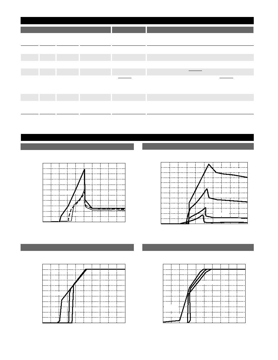
V
OUT
vs V
IN
over Temperature
I
CQ
vs. V
IN
over R
LOAD
I
CQ
vs. V
IN
over Temperature
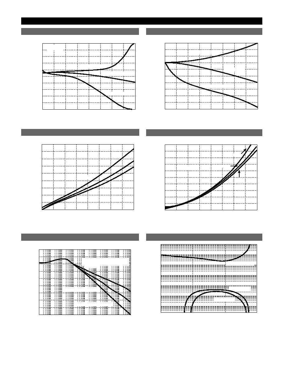
0.0
0.0
V
OUT
(V)
V
IN
(V)
1.0
2.0
3.0
4.0
5.0
6.0
7.0
8.0
9.0
10.0
0.5
1.0
1.5
2.0
2.5
3.0
3.5
4.0
4.5
5.0
5.5
Room Temp.
Rload =
NO LOAD
Rload = 6.67
Rload = 10
V
OUT
vs. V
IN
over R
LOAD
Package Lead Description
PACKAGE LEAD #
LEAD SYMBOL
FUNCTION
CS8126, -1, -2
5 Lead TO-220
7Lead
16 Lead
8126-1 8126-2
D
2
PAK
SOIC Wide
1
1
1
1
V
IN
Unregulated supply voltage to IC.
2
5
2
16
V
OUT
Regulated 5V output.
3
3
4
11
Gnd
Ground connection.
4
4
5
8
Delay
Timing capacitor for
function.
5
2
6
6
CMOS/TTL compatible output lead.
goes low
after detection of any error in the regulated output or
during power up.
3
14
V
OUT(SENSE)
Remote sensing of output voltage.
7
2, 3, 4, 5, 7, 9,
NC
No Connection.
10, 12, 13, 15
RESET
RESET
RESET
4
0
0
Dropout V
oltage (mV)
Output Current (mA)
100
200
300
400
500
600
700
800
100
200
300
400
500
600
700
800
900
25˚C
-40˚C
125˚C
0
0
Quiescent Current (mA)
Output Current (mA)
10
20
30
40
50
60
70
80
90
100
100
200
300
400
500
600
700
800
V
IN
= 14V
125˚C
25˚C
-40˚C
0
10
0
Rejection (dB)
Freq. (Hz)
10
1
10
2
10
3
10
4
10
5
10
6
10
7
10
8
10
20
30
40
50
60
70
80
90
I
OUT
= 250mA
C
OUT
= 10
mF, ESR = 10W
C
OUT
= 10
mF, ESR = 1W
C
OUT
= 10
mF, ESR = 1 & 0.1mF,
ESR = 0
Ripple Rejection
Quiescent Current vs. Output Current over Temperature
Dropout Voltage vs. Output Current over Temperature
Typical Performance Characteristics: continued
-100
0
Line Regulation (mV)
Output Current (mA)
-80
-60
-40
-20
0
20
40
60
80
100
100
200
300
400
500
600
700
800
V
IN
6-26V
TEMP = 25˚C
TEMP = 40˚C
TEMP = 125˚C
-14
0
Load Regulation (mV)
Output Current (mA)
-12
-10
-8
-6
-4
-2
0
2
4
6
100
200
300
400
500
600
700
800
TEMP = 25˚C
TEMP = 125˚C
V
IN
= 14V
TEMP = -40˚C
Load Regulation vs. Output Current over Temperature
Line Regulation vs. Output Current over Temperature
10
0
ESR (ohms)
Output Current (mA)
10
1
10
2
10
3
10
1
10
2
10
3
10
-4
10
0
10
-1
10
-2
10
-3
C
OUT
= 68
mF
C
OUT
= 47
mF
C
OUT
= 47/68
mF
Stable Region
Output Capacitor ESR
CS8126, -1, -2
5
The CS8126
function, has hysteresis on both the
Reset and Delay comparators, a latching Delay capacitor
discharge circuit, and operates down to 1V.
The
circuit output is an open collector type with
ON and OFF parameters as specified. The
output
NPN transistor is controlled by the two circuits described
(see Block Diagram).
Low Voltage Inhibit Circuit
This circuit monitors output voltage, and when the output
voltage falls below V
RT(OFF)
, causes the
output tran-
sistor to be in the ON (saturation) state. When the output
voltage rises above V
RT(ON)
, this circuit permits the
output transistor to go into the OFF state if allowed by
the
Delay circuit.
RESET Delay Circuit
This circuit provides a programmable (by external capaci-
tor) delay on the
output lead. The Delay lead pro-
vides source current to the external delay capacitor only
when the "Low Voltage Inhibit" circuit indicates that out-
put voltage is above V
RT(ON)
. Otherwise, the Delay lead
sinks current to ground (used to discharge the delay
capacitor). The discharge current is latched ON when the
output voltage falls below V
RT(OFF)
. The Delay capacitor is
fully discharged anytime the output voltage falls out of
regulation, even for a short period of time. This feature
ensures a controlled
pulse is generated following
detection of an error condition. The circuit allows
the
output transistor to go to the OFF (open) state
only when the voltage on the Delay lead is higher than
V
DC(H1)
.
The Delay time for the
function is calculated from
the formula:
Delay time =
Delay time = C
Delay
¥ 3.2 ¥ 10
5
If C
Delay
= 0.1µF, Delay time (ms) = 32ms ± 50%: i.e. 16ms
to 48ms. The tolerance of the capacitor must be taken into
account to calculate the total variation in the delay time.
C
Delay
¥ V
Delay
Threshold
I
Charge
RESET
RESET
RESET
RESET
RESET
RESET
RESET
RESET
RESET
RESET
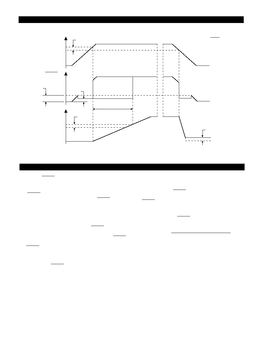
RESET Circuit Waveform
V
RH
V
OUT
V
RT(ON)
V
RT(OFF)
V
RL
Delay
V
DC(HI)
V
DC(LO)
V
DH
t
Delay
V
DIS
(3)
(1)
(2)
(2)
RESET
(1) = No Delay Capacitor
(2) = With Delay Capacitor
(3) = Max: RESET Voltage (1.0V)
Circuit Description
CS8126, -1, -2