 | –≠–ª–µ–∫—Ç—Ä–æ–Ω–Ω—ã–π –∫–æ–º–ø–æ–Ω–µ–Ω—Ç: CS8135 | –°–∫–∞—á–∞—Ç—å:  PDF PDF  ZIP ZIP |
1
Features
s
Two Regulated Outputs
Primary Output 5V
± 5%; 500mA
Secondary Standby 5V
±5%; 10mA
s
Low Dropout Voltage
(0.6V at 0.5A)
s
ON/OFF Control
Option
s
Low Quiescent Drain
(<3mA)
s
RESET Option
s
Protection Features
Reverse Battery
60V Load Dump
-50V Reverse Transient
Short Circuit
Thermal Shutdown
Overvoltage Shutdown
Package Option
5 Lead TO-220
Tab (Gnd)
1
CS8135
5V, 5V Low Dropout Dual Regulator
with
/ENABLE
RESET
CS8135
Description
V
IN
V
OUT2
Gnd
V
OUT1
RESET/
ENABLE
Output
Current
Limit
+
-
Output
Current
Limit
Over Voltage
Shutdown
+
-
+
-
Primary Output
Standby Output
+
-
Thermal
Shutdown
Bandgap
Reference
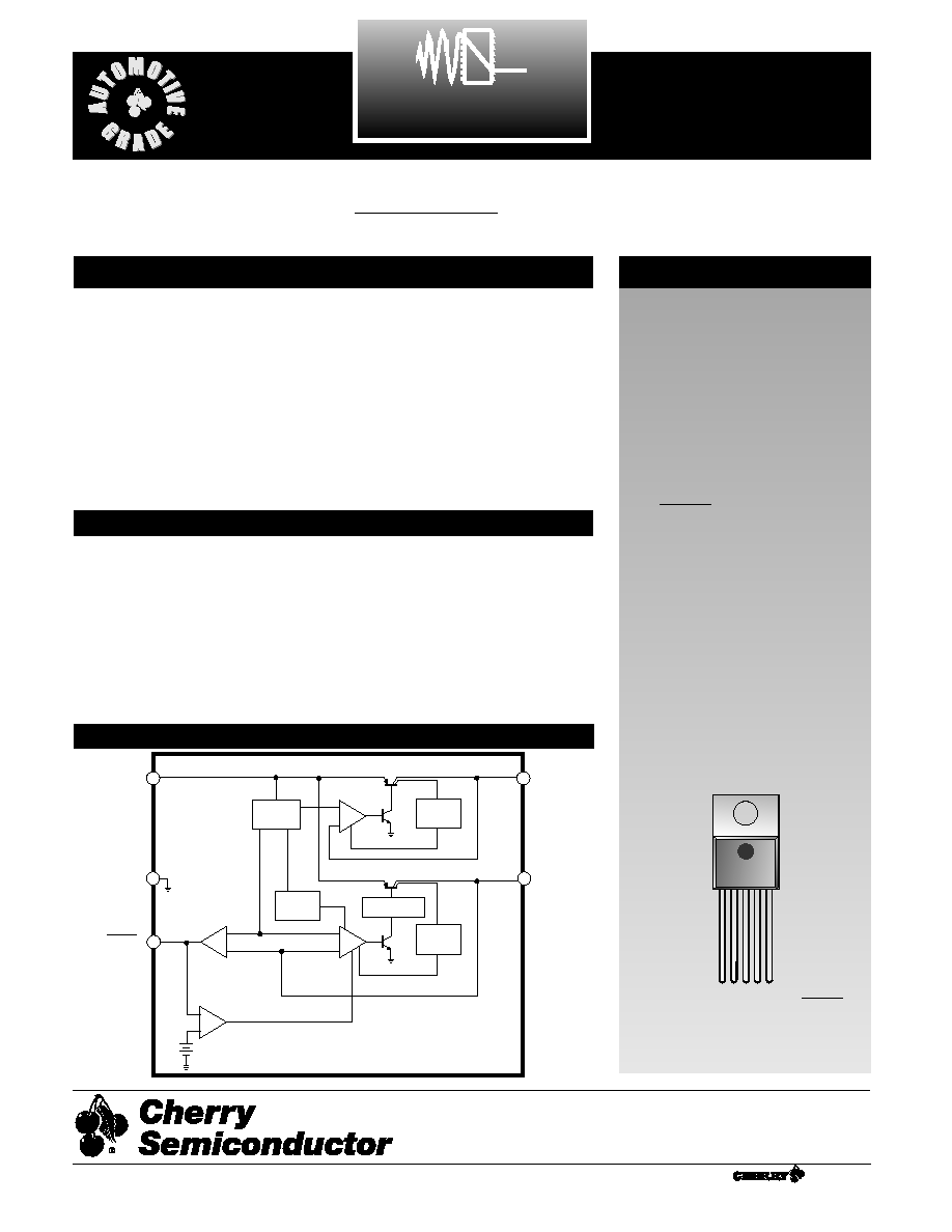
Block Diagram
Absolute Maximum Ratings
Input Voltage
Operating Range .....................................................................-0.5V to 26V
Load Dump ............................................................................................60V
Internal Power Dissipation ..................................................Internally Limited
Junction Temperature Range (T
J
)............................................-40°C to +150°C
Storage Temperature Range ....................................................-65°C to +150°C
Lead Temperature Soldering
Wave Solder (through hole styles only)..........10 sec. max, 260°C peak
Electrostatic Discharge (Human Body Model) ..........................................2kV
The CS8135 is a low dropout, high cur-
rent, dual 5V linear regulator. The sec-
ondary 5V/10mA output is often used
for powering systems with standby
memory. Quiescent current drain is
less than 3mA when supplying 10mA
loads from the standby regulator.
In automotive applications, the CS8135
and all regulated circuits are protected
from reverse battery installations, as
well as two-battery jumps. During line
transients, such as a 60V load dump,
the 500mA output will automatically
shut down the primary output to pro-
tect both internal circuits and the load.
The standby regulator will continue to
power any standby load.
The CS8135 is packaged in a 5 lead
TO-220.
NOTE: The CS8135 is compatible with
the LM2935.
1 V
IN
2 V
OUT1
3 Gnd
4
/
ENABLE
5 V
OUT2
RESET
A Company
®
Rev. 10/21/97
Cherry Semiconductor Corporation
2000 South County Trail, East Greenwich, RI 02818
Tel: (401)885-3600 Fax: (401)885-5786
Email: info@cherry-semi.com
Web Site: www.cherry-semi.com

2
CS8135
PARAMETER
TEST CONDITIONS
MIN
TYP
MAX
UNIT
Electrical Characteristics :
V
IN
= 14V, I
OUT1
= 5mA, I
OUT2
= 1mA, -40°C ≤ T
A
≤ 125°C, -40°C ≤ T
J
≤ 150°C unless otherwise specified
s Output Stage (V
OUT1
)
Output Voltage, V
OUT1
6V ≤ V
IN
≤ 26V, 5mA ≤ I
OUT1
≤ 500mA
4.75
5.00
5.25
V
Dropout Voltage
I
OUT
= 500mA
0.35
0.60
V
I
OUT
= 750mA
0.50
V
Line Regulation
6V ≤ V
IN
≤ 26V, I
OUT1
= 5mA
10
50
mV
Load Regulation
5mA ≤ I
OUT
≤ 500mA
10
50
mV
Quiescent Current
I
OUT1
≤ 10mA, No Load on Standby
3
7
mA
I
OUT1
= 500mA, No Load on Standby
30
100
mA
I
OUT1
= 750mA, No Load on Standby
60
150
mA
Ripple Rejection
f = 120Hz
66
dB
Current Limit
0.75
1.40
A
Maximum Line Transient
V
OUT1
≤ 5.5V
90
V
Reverse Polarity
V
OUT1
≥ -0.6V, 10Ω Load
-50
V
Input Voltage, DC
Reverse Polarity Input
1% Duty Cycle, t = 100ms, V
OUT1
≥ -6V,
-80
V
Voltage, Transient
10Ω Load
Output Noise Voltage
10Hz-100kHz
100
µVrms
Long Term Stability
20
mV/khr
Output Impedance
500mA DC and 10mA rms,
200
mΩ
100Hz-10kHz
Overvoltage Shutdown
30
V
s Standby Output (V
OUT2
)
Output Voltage (V
OUT2
)
6V ≤ V
IN
≤ 26V, 1mA ≤ I
OUT1
≤ 10mA
4.75
5.00
5.25
V
Dropout Voltage
I
OUT2
= 10mA
0.3
0.7
V
Tracking
V
OUT1
-V
OUT2
50
200
mV
Line Regulation
6V ≤ V
IN
≤ 26V
4
50
mV
Load Regulation
1mA ≤ I
OUT1
≤ 10mA
10
50
mV
Quiescent Current
I
OUT
≤ 10mA, V
OUT
OFF 2
3
mA
Ripple Rejection
f = 120Hz
66
dB
Current Limit
25
70
mA
Output Noise Voltage
10Hz-100kHz
300
µV
Long Term Stability
20
mV/khr
Output Impedance
10mA DC and 1mA rms, 100Hz-10kHz
1
Ω
s
Function
Output Voltage
Low R
1
= 20kΩ, V
IN
= 4.5V
See Test & Application Circuit
0.8
1.1
V
High R
1
= 20kΩ, V
IN
= 14V
(page 6)
4.5
5.0
6.0
V
Output Current
V
IN
= 4.5V,
in Low State
5
mA
ON/OFF Resistor
R1 (±10% Tolerance)
20
30
kΩ
RESET
RESET
RESET
RESET
3
CS8135
Package Lead Description
PACKAGE LEAD #
LEAD SYMBOL
FUNCTION
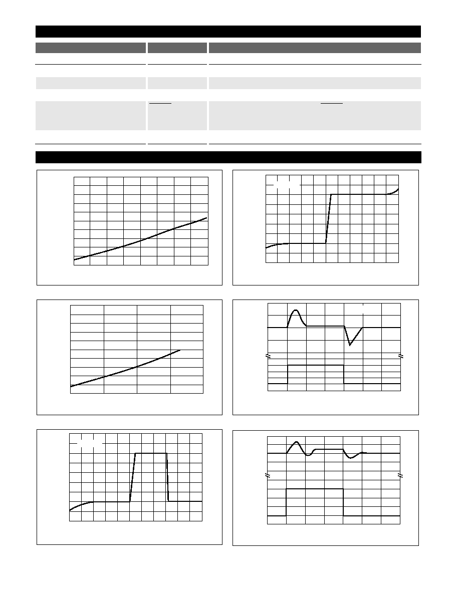
Typical Performance Characteristics
TO-220
1
V
IN
Supply voltage to IC, usually direct from battery.
2
V
OUT1
Regulated output voltage 5V, 500mA (typ) switched.
3
Gnd
Ground connection.
4
/ENABLE
CMOS compatible output lead,
goes low whenever
V
OUT1
becomes unregulated. To use the ENABLE option, con-
nect the lead via a resistor to V
IN
(see app. notes).
5
V
OUT2
STANDBY output 5V, 10mA typ, always on.
RESET
RESET
Dropout Voltage vs. Output Current
Standby Dropout Voltage vs. Output Current
Output Voltage vs. Input Voltage
Standby Output Voltage vs. Input Voltage
Line Transient Response (V
OUT1
)
Line Transient Response (V
OUT2
)
10
TIME (
ms)
INPUT
VOL
T
AGE
CHANGE (V)
OUTPUT
VOL
T
AGE
DEVIA
TION (mV)
5
0
-5
-10
3
2
1
0
0
10
20
30
40
50
60
20
10
0
-10
-20
3
2
1
0
0
10
20
30
40
50
60
TIME (
ms)
INPUT
VOL
T
AGE
CHANGE (V)
OUTPUT
VOL
T
AGE
DEVIA
TION (mV)
I
OUT
1
=500mA
7
6
5
4
3
2
1
0
-1
-2
-40
-20
0
20
40
60
INPUT VOLTAGE (V)
OUTPUT
VOL
T
AGE (V)
R
L
=500
W
7
6
5
4
3
2
1
0
-1
-2
-40
-20
0
20
40
60
INPUT VOLTAGE (V)
OUTPUT
VOL
T
AGE (V)
R
L
=10
W
1.0
0.9
0.8
0.7
0.6
0.5
0.4
0.3
0.2
0.1
0.0
INPUT
-OUTPUT
DIFFERENTIAL
VOL
T
AGE (V)
OUTPUT CURRENT (mA)
0
5
10
15
20
1.0
0.9
0.8
0.7
0.6
0.5
0.4
0.3
0.2
0.1
0.0
INPUT
-OUTPUT
DIFFERENTIAL
VOL
T
AGE (V)
OUTPUT CURRENT (mA)
0
200
400
600
800
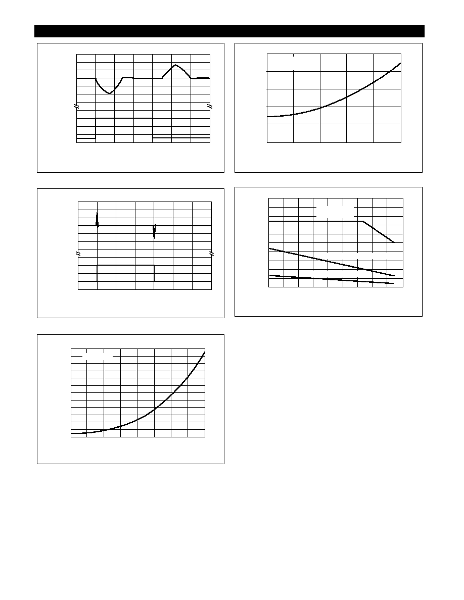
Load Transient Response (V
OUT1
)
Load Transient Response (V
OUT2
)
Quiescent Current vs. Output Current
Quiescent Current vs. Standby Output Current
Maximum Power Dissipation (TO-220)
AMBIENT TEMPERATURE (
∞C)
POWER DISSIP
A
TION (W)
20
0
18
16
14
12
10
8
6
4
2
0
10
20
30
40
50
60
70
80
90
INFINITE
HEAT SINK
10
∞ C/W HEAT SINK
NO HEAT SINK
STANDBY OUTPUT CURRENT (mA)
QUIESCENT
CURRENT
(mA)
0
5
4
3
2
1
0
5
10
15
20
25
SWITCH OPEN
V
O
OFF
OUTPUT CURRENT (mA)
QUIESCENT
CURRENT
(mA)
0
120
100
80
60
40
20
0
200
400
600
800
I
OUT2
=10mA
150
TIME (
ms)
ST
ANDBY
LOAD
CURRENT
(mA)
ST
ANDBY
OUTPUT
VOL
T
AGE
DEVIA
TION (mV)
100
50
0
-50
-100
-150
20
15
10
5
0
0
10
20
30
40
50
60
150
TIME (
ms)
LOAD
CURRENT
(A)
OUTPUT
VOL
T
AGE
DEVIA
TION (mV)
100
50
0
-50
-100
-150
0.8
0.6
0.4
0.2
0
0
10
20
30
40
50
60
4
Typical Performance Characteristics: continued
CS8135
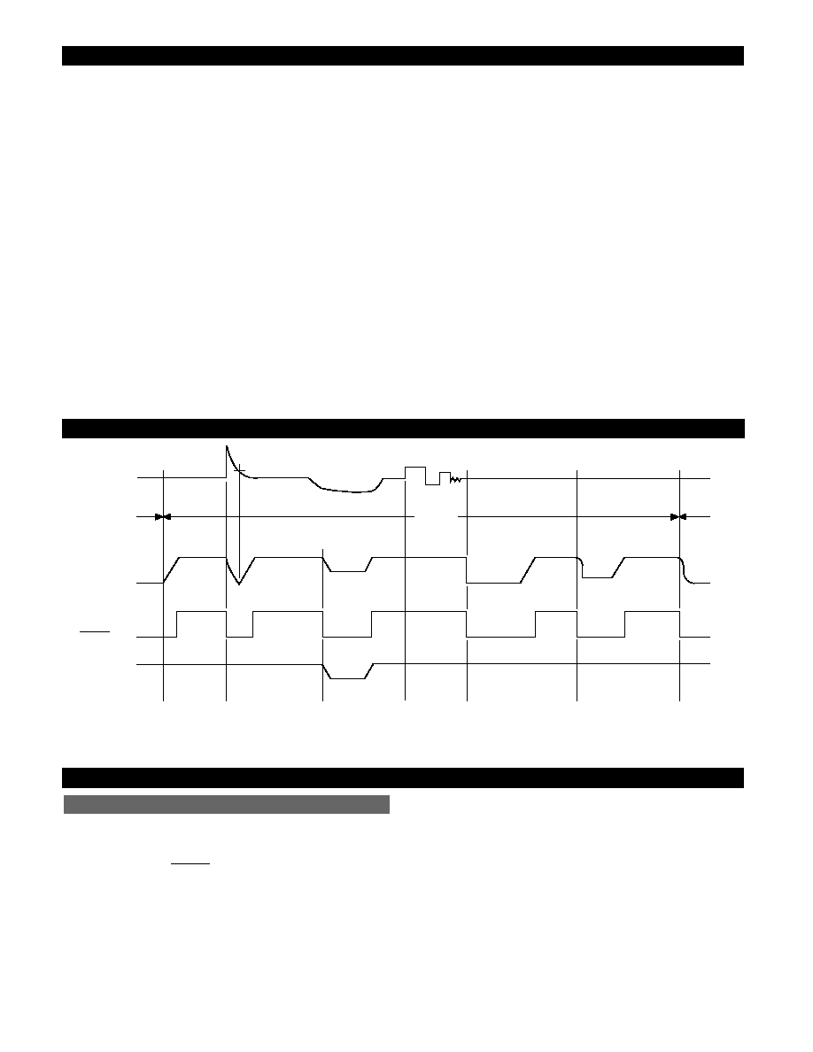
V
IN
SWITCH
V
OUT
1
RESET
V
OUT
2
System
Condition
5V
0V
0V
OPEN
14V
5V
5V
60V
31V
3V
2.4V
26V
CLOSED
5V
0V
2.4V
Turn
On
Load
Dump
Low V
IN
Line, Noise, Etc.
V
OUT1
Short
Circuit
Thermal
Shutdown
Turn
Off
5V
5V
5V
0V
O P E N
14V
5V
Typical Circuit Waveform
*Reference Test & Application Circuit
The CS8135 is equipped with two outputs. The second out-
put is intended for use in systems requiring standby mem-
ory circuits. While the high current regulator output can be
controlled with the
lead described below, the stand-
by output remains on under all conditions as long as suffi-
cient input voltage is applied to the IC. Thus, memory and
other circuits powered by this output remain unaffected by
positive line transients, thermal shutdown, etc.
The standby regulator circuit is designed so that the quies-
cent current to the IC is very low (<3mA) when the other
regulator output is off.
In applications where the standby output is not needed, it
may be disabled by connecting a resistor from the standby
output to the supply voltage. This eliminates the need for
a capacitor on the output to prevent unwanted oscilla-
tions. The value of the resistor depends upon the mini-
mum input voltage expected for a given system. Since the
standby output is shunted with an internal diode zener,
the current through the external resistor should be suffi-
cient to bias V
OUT2
up to this point. Approximately 60µA
will suffice, resulting in a 10kΩ external resistor for most
applications.
RESET
Standby Output
5
Circuit Description
CS8135
Dropout Voltage
The input-output voltage differential at which the circuit
ceases to regulate against further reduction in input volt-
age. Measured when the output voltage has dropped
100mV from the nominal value obtained at 14V input,
dropout voltage is dependent upon load current and junc-
tion temperature.
Input Voltage
The DC voltage applied to the input with respect to ground.
Input Output Differential
The voltage difference between the unregulated input
voltage and the regulated output voltage for which the
regulator will operate.
Line Regulation
The change in output voltage for a change in the input
voltage. The measurement is made under conditions of
low dissipation or by using pulse techniques such that the
average chip temperature is not significantly affected.
Load Regulation
The change in output voltage for a change in load current
at constant chip temperature.
Long Term Stability
Output voltage stability under accelerated life-test condi-
tions after 1000 hours with maximum rated voltage and
junction temperature.
Output Noise Voltage
The rms AC voltage at the output, with constant load and
no input ripple, measured over a specified frequency
range.
Quiescent Current
The part of the positive input current that does not con-
tribute to the positive load current. i.e., the regulator
ground lead current.
Ripple Rejection
The ratio of the peak-to-peak input ripple voltage to the
peak-to-peak output ripple voltage.
Temperature Stability of V
OUT
The percentage change in output voltage for a thermal
variation from room temperature to either temperature
extreme.
Current Limit
Peak current that can be delivered to the output.
Definition of Terms