 | –≠–ª–µ–∫—Ç—Ä–æ–Ω–Ω—ã–π –∫–æ–º–ø–æ–Ω–µ–Ω—Ç: CS8141YT7 | –°–∫–∞—á–∞—Ç—å:  PDF PDF  ZIP ZIP |
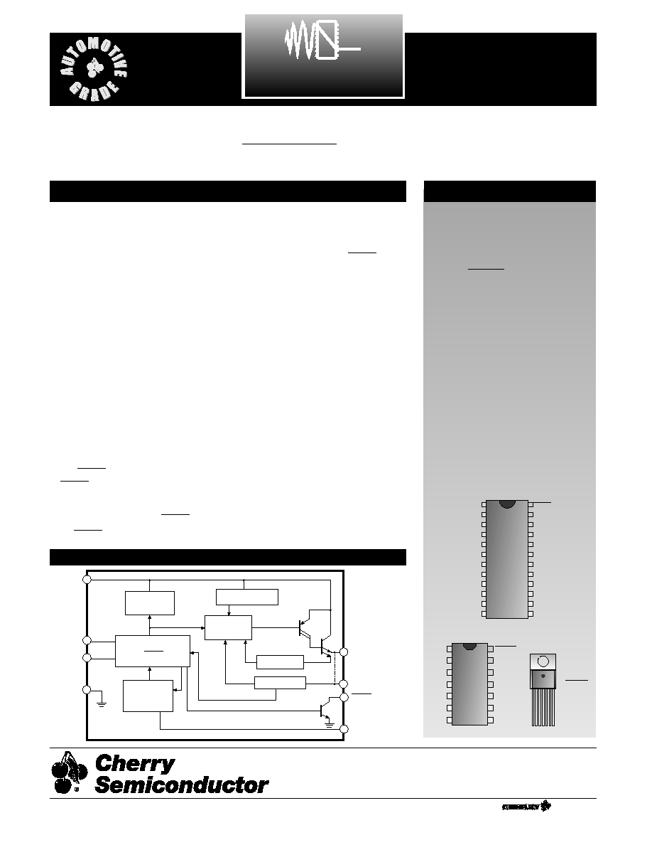
The CS8140 is a 5V Watchdog
Regulator with protection circuitry and
three logic control functions that allow
a microprocessor to control its own
power supply. The CS8140 is designed
for use in automotive, switch mode
power supply post regulator, and bat-
tery powered systems.
Basic regulator performance character-
istics include a low noise, low drift, 5V
± 4% precision output voltage with low
dropout voltage (1.25V @ I
OUT
= 500mA)
and low quiescent current (7mA @ I
OUT
= 500mA). On board short circuit, ther-
mal, and overvoltage protection make it
possible to use this regulator in particu-
larly harsh operating environments.
The Watchdog logic function monitors
an input signal (WDI) from the micro-
processor or other signal source. When
the signal frequency moves outside
externally programmable window lim-
its, a
signal is generated
(
). An external capacitor
(C
DELAY
) programs the watchdog win-
dow frequency limits as well as the
power on reset (POR) and
delay.
The
function is activated by any
of three conditions: the watchdog sig-
nal moves outside of its preset limits;
the output voltage drops out of regula-
tion by more than 4.5%; or the IC is in
its power up sequence. The
sig-
nal is independent of V
IN
and reliable
down to V
OUT
= 1V.
In conjunction with the Watchdog, the
ENABLE function controls the regula-
tor’s power consumption. The CS8140’s
output stage and its attendant circuitry
are enabled by setting the ENABLE
lead high. The regulator goes into sleep
mode (I
OUT
= 250µA) when the
ENABLE lead goes low and the watch-
dog signal moves outside its preset
window limits. This unique combina-
tion of control functions in the CS8140
gives the microprocessor control over
its own power down sequence: i.e. it
gives the microprocessor the flexibility
to perform housekeeping functions
before it powers down.
The CS8141 has the same features as the
CS8140, except that the CS8141 only
responds to input signals (WDI) which
are below the preset watchdog frequen-
cy threshold.
RESET
RESET
RESET
RESET
RESET
1
Features
Gnd
WDI
ENABLE
VIN
VOUT
Delay
Overvoltage
Overtemperature
Reference
& Bias
Short Circuit
Watchdog
Undervoltage
Regulation
RESET
Control Logic
ENABLE
RESET
Delay
Sense
*NOTE: shorted together
on 7 Lead TO-220
*
s
5V ± 4%, 500mA Output
Voltage
s
µP Compatible Control
Functions
Watchdog
ENABLE
s
Low Dropout Voltage
(1.25V @ 500mA)
s
Low Quiescent Current
(7mA @ 500mA)
s
Low Noise, Low Drift
s
Low Current SLEEP Mode
(I
Q
= 250µA)
s
Fault Protection
Thermal Shutdown
Short Circuit
60V Peak Transient
Voltage
RESET
Package Options
7 Lead TO-220
Tab (Gnd)
14 Lead PDIP
24 Lead SOIC Wide
CS8140/1
5V, 500mA Linear Regulator with
ENABLE,
, and Watchdog
RESET
1
1
Delay
V
OUT
Sense
WDI
NC
NC
NC
NC
NC
V
IN
ENABLE
RESET
Gnd
NC
NC
NC
Gnd
NC
NC
NC
NC
NC
NC
NC
CS8140/1
Description
Block Diagram
1
Delay
V
OUT
Sense
WDI
NC
NC
NC
NC
NC
Gnd
V
IN
ENABLE
RESET
NC
1 V
IN
2 ENABLE
3
4 Gnd
5 Delay
6 WDI
7 V
OUT
RESET
A Company
®
Rev. 2/23/99
Cherry Semiconductor Corporation
2000 South County Trail, East Greenwich, RI 02818
Tel: (401)885-3600 Fax: (401)885-5786
Email: info@cherry-semi.com
Web Site: www.cherry-semi.com

2
Electrical Characteristics:
7V ≤ V
IN
≤ 26V, 5mA ≤ I
OUT
≤ 500mA, -40˚C ≤ T
J
≤ +150˚C, -40˚C ≤ T
A
≤ 125˚C
unless otherwise specified
PARAMETER
TEST CONDITIONS
MIN
TYP
MAX
UNIT
Absolute Maximum Ratings
Input Voltage
Operating Range .................................................................................................................................................-0.5 to +26V
Peak Transient Voltage (46V Load Dump @ 14V V
BAT
) ..............................................................................................60V
Electrostatic Discharge
(Human Body Model)...............................................................................................................................................4kV
WDI Input Signal Range ...............................................................................................................................................-0.3 to +7V
Internal Power Dissipation ..............................................................................................................................Internally limited
Junction Temperature Range (TJ) .......................................................................................................................-40°C to +150°C
Storage Temperature Range ................................................................................................................................-65°C to +150°C
Lead Temperature Soldering
Wave Solder (through hole styles only) .....................................................................................10 sec. max, 260°C peak
Reflow (SMD styles only) ......................................................................................60 sec. max above 183°C, 230°C peak
ENABLE .......................................................................................................................................................................-0.3V to V
IN
CS8140/1
s Output Stage (V
OUT
)
Output Voltage, V
OUT
7V ≤ V
IN
≤ 26V
4.8
5.0
5.2
V
5mA < I
OUT
< 500mA
Dropout Voltage (V
IN
- V
OUT
)
I
OUT
= 500mA
1.25
1.50
V
Line Regulation
I
OUT
= 50mA,
5
25
mV
7V ≤ V
IN
≤ 26V
Load Regulation
V
IN
= 14V,
5
80
mV
50mA ≤ I
OUT
≤ 500mA
Output Impedance, R
OUT
500mA DC and 10mA AC ,
200
mΩ
100Hz ≤ f ≤ 10kHz
Quiescent Current, (I
Q
)
Active Mode
0 ≤ I
OUT
≤ 500mA, 7V ≤ V
IN
≤ 26V
7.00
15.00
mA
Sleep Mode
I
OUT
= 0mA, V
IN
= 13V, ENABLE = 0V
0.25
0.50
mA
Ripple Rejection
7 ≤ V
IN
≤ 17V, I
OUT
= 250mA,
60
75
dB
f = 120Hz
Current Limit
700
1200
2000
mA
Thermal Shutdown
150
180
°C
Overvoltage Shutdown
V
OUT
< 1V
30
34
38
V
s ENABLE
Threshold
HIGH
V
OUT
≥ 0.5V, (V
OUT(ON)
)
4.05
4.50
V
LOW
V
OUT
< 0.5V, (V
OUT(OFF)
)
3.50
3.95
V
Threshold Hysteresis
(HIGH - LOW)
100
mV
3
Package Lead Description
Package Lead #
Lead Symbol
Function
Electrical Characteristics: continued
PARAMETER
TEST CONDITIONS
MIN
TYP
MAX
UNIT
CS8140/1
s
Threshold
HIGH V
R(HI)
V
OUT
increasing
4.65
4.90 V
OUT
- 0.05
V
LOW V
R(LOW)
V
OUT
decreasing
4.50
4.70
4.90
V
Threshold Hysteresis(V
RH
)
(HIGH - LOW)
150
200
250
mV
Reset Output Leakage
V
OUT
≥ V
R(HI)
25
µA
= HIGH
Output Voltage
Low(V
L(LOW)
)
1V ≤ V
OUT
≤ V
R(LOW)
0.1
0.4
V
Rp = 2.7kΩ*
Low (V
Rpeak
)
V
OUT
, Power up, Power down
0.6
1.0
V
Delay Times
C
DELAY
= 0.1µF
t
POR
30.0
47.5
65.0
ms
t
WDI(
)
0.5
1.0
1.5
ms
s Watchdog
Input Voltage
HIGH
2.0
V
LOW
0.8
V
Input Current
WDI ≤ V
OUT
0
10
µA
Threshold Frequency
C
DELAY
= 0.1µF
f
WDILOWER
64
77
96
Hz
f
WDI(UPPER)
**
218
262
326
Hz
* R
P
is connected to
and V
OUT
.
** CS8140 only
To observe safe operating junction temperature, low duty cycle pulse testing is used on tests where applicable.
RESET
RESET
RESET
RESET
7 Lead
24 Lead *
14 Lead
TO-220
SOIC Wide
PDIP
1
21
12
V
IN
Supply voltage to IC, usually direct from the battery.
2
23
13
ENABLE
CMOS compatible logical input. V
OUT
is disabled when
ENABLE is LOW and WDI is beyond its preset limits.
3
24
14
CMOS compatible output lead.
goes low whenever
V
OUT
drops below 4.5% of its typical value for more than
2µs or WDI signal falls outside it’s window limits.
4
12, 20
11
Gnd
Ground connection.
5
2
1
Delay
Timing capacitor for Watchdog and
functions.
6
3
2
WDI
CMOS compatible input lead. The Watchdog function mon-
itors the falling edge of the incoming digital pulse train. The
signal is usually generated by the system microprocessor.
7
4
3
V
OUT
Regulated output voltage, 5V (typ).
N/A
5
4
Sense
Kelvin connection which allows remote sensing of output
voltage for improved regulation.
1,6-11,13-19,22
5-10
NC
No connection.
* The CS8141 uses a fused lead package. Leads 6-8 and 17-19 are fused together through the lead frame. These leads are
electrically connected to IC ground and should be connected to system ground for a good thermal connection.
RESET
RESET
RESET
4
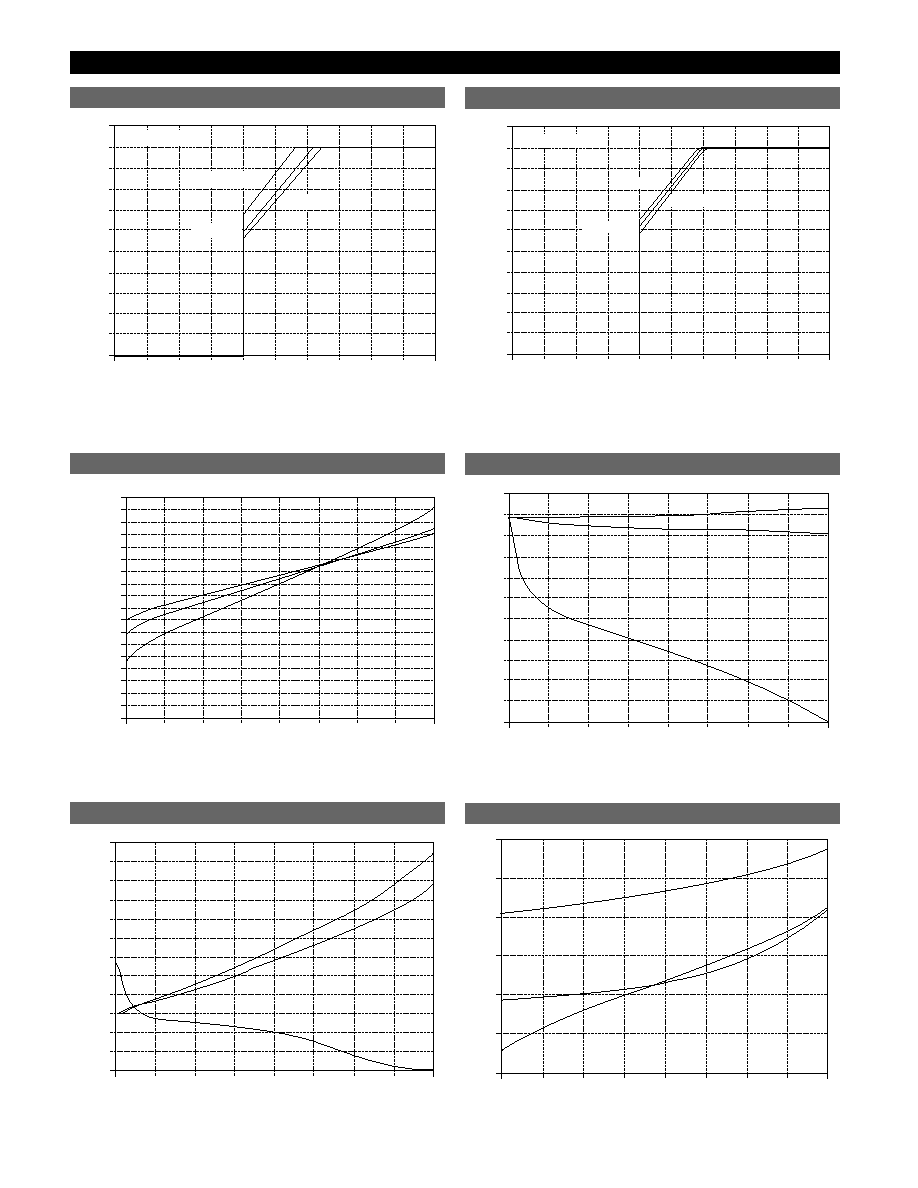
Typical Performance Characteristics
CS8140/1
0
1
2
3
4
5
6
7
8
9
10
0.0
0.5
1.0
1.5
2.0
2.5
3.0
3.5
4.0
4.5
5.0
5.5
R
load
= NO LOAD
V
OUT
(V)
V
IN
(V)
V
ENABLE
= V
IN
R
load
= 6.67
W
R
load
= 10
W
V
OUT
vs. V
IN
over R
LOAD
; T = 25˚C
0
1
2
3
4
5
6
7
8
9
10
0.0
0.5
1.0
1.5
2.0
2.5
3.0
3.5
4.0
4.5
5.0
5.5
V
OUT
(V)
V
IN
(V)
TEMP = 25
∞C
TEMP = 125
∞C
TEMP = -40
∞C
V
ENABLE
= V
IN
V
OUT
vs. V
IN
over Temperature; R
LOAD
= 25Ω
0
100
200
300
400
500
600
700
800
0
400
600
800
1200
1400
1600
1800
200
1000
-40
∞C
125
∞C
25
∞C
I
OUT
(mA)
Dropout V
oltage (mV)
Dropout Voltage vs. Output Current over Temperature
0
100
200
300
400
500
600
700
800
-35.0
-31.5
-28.0
-24.5
-21.0
-17.5
-14.0
-10.5
-7.0
-3.5
0
3.5
-40
∞C
25
∞C
125
∞C
V
IN
= 14V
I
OUT
(mA)
LOAD REGULA
TION (mV)
Load Regulation vs. Output Current over Temperature
0
100
200
300
400
500
600
700
800
-6
-4
-2
0
2
4
6
8
10
12
14
18
-40
∞C
25
∞C
125
∞C
V
IN
= 14V
I
OUT
(mA)
16
LINE REGULA
TION (mV)
Line Regulation vs. Output Current over Temperature
0
100
200
300
400
500
600
700
800
4
5
6
7
8
9
10
-40
∞C
125
∞C
25
∞C
I
OUT
(mA)
I
Q
(mA)
V
IN
= 14V
Quiescent Current vs. Output Current over Temperature
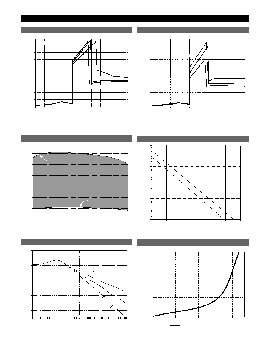
5
Typical Performance Characteristics: continued
CS8140/1
0
1
2
3
4
5
6
7
8
9
10
0
2
4
8
10
12
14
16
18
20
V
IN
(V)
I
Q
(mA)
6
R
load
= NO LOAD
R
load
= 6.67
R
load
= 25
V
ENABLE
= V
IN
Quiescent Current vs. V
IN
over R
LOAD
; T = 25°C
0
1
2
3
4
5
6
7
8
9
10
0
2
4
8
10
12
14
16
18
20
TEMP = 125
∞C
TEMP = 25
∞C
TEMP =- 40
∞C
V
IN
(V)
I
Q
(mA)
6
V
ENABLE
= V
IN
Quiescent Current vs. V
IN
over Temperature; R
LOAD
= 25Ω
-40 -30
-10
10
20
40
60
70
90
110 120
60
80
100
120
140
160
180
200
220
240
260
280
-20
0
30
50
80
100
130 140 150
300
T
J
(
∞C)
FREQUENCY
(Hz)
Lower Threshold
C
DELAY
= 0.1
m
F
Upper Threshold
Watchdog Frequency Thresholds vs. Temperature
10
5
10
4
10
3
10
2
10
1
10
0
10
1
10
2
10
3
10
4
10
5
10
6
CAPACITANCE (pF)
WDI THRESHOLD
10
6
Lower Threshold
10
7
10
7
Upper Threshold
Watchdog Frequency Threshold vs C
DELAY
90
80
70
60
50
40
30
20
10
0
REJECTION (dB)
FREQUENCY (Hz)
C
O
= 10
mF, ESR=10W
C
O
= 10
mF,ESR=1W
C
O
= 10
mF, ESR=1&0.1mF, ESR=0
I
O
=250mA
10
0
10
1
10
2
10
3
10
4
10
5
10
6
10
7
10
8
Ripple Rejection vs Frequency
2000
1800
1600
1400
1200
1000
800
600
400
200
0
1
5
10
15
20
25
30
35
40
V
IN
= 5V
RESET OUTPUT CURRENT (mA)
RESET
OUTPUT
VOL
T
AGE (mV)
RESET Output Voltage vs Output Current
Precision Voltage Reference
The regulated output voltage depends on the precision
band gap voltage reference in the IC. By adding an error
amplifier into the feedback loop , the output voltage is main-
tained within ±4% over temperature and supply variation.
Output Stage
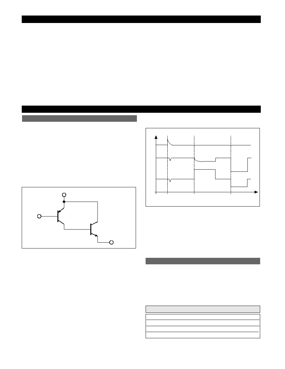
The composite PNP-NPN output structure (Figure1) pro-
vides 500mA (min) of output current while maintaining a
low drop out voltage (1.25V) and drawing little quiescent
current (7mA).
Figure 1: Composite Output Stage of the CS8140/1
The NPN pass device prevents deep saturation of the out-
put stage which in turn improves the IC’s efficiency by
preventing excess current from being used and dissipated
by the IC.
Output Stage Protection
The output stage is protected against overvoltage, short
circuit and thermal runaway conditions (Figure 2).
If the input voltage rises above 30V (e.g. load dump), the
output shuts down. This response protects the internal cir-
cuitry and enables the IC to survive unexpected voltage
transients.
Using an emitter sense scheme, the amount of current
through the NPN pass transistor is monitored. Feedback
circuitry insures that the output current never exceeds a
preset limit.
Figure 2: Typical Circuit Waveforms for Output Stage Protection.
Should the junction temperature of the power device
exceed 180˚C (typ), the power transistor is turned off.
Thermal shutdown is an effective means to prevent die
overheating since the power transistor is the principle heat
source in the IC.
The CS8140 differs from all other linear regulators in its
unique combination of control features.
Watchdog and ENABLE Functions
V
OUT
is controlled by the logic functions ENABLE and
Watchdog (Table 1).
Table 1: V
OUT
as a Function of ENABLE and Watchdog
WDI
ENABLE
Slow
Normal
Fast
High
Low
H
5
5
5
5
5
L
0
5
0
0
0
V
OUT
(V)
Regulator Control Functions
I
O
V
OUT
V
IN
Load
Dump
Short
Circuit
Thermal
Shutdown
> 30V
V
OUT
V
IN
Voltage Reference and Output Circuitry
6
CS8140/1
Dropout Voltage
The input-output voltage differential at which the circuit
ceases to regulate against further reduction in input volt-
age. Measured when the output voltage has dropped
100mV from the nominal value obtained at 14V input,
dropout voltage is dependent upon load current and junc-
tion temperature.
Input Voltage
The DC voltage applied to the input terminals with respect
to ground.
Line Regulation
The change in output voltage for a change in the input
voltage. The measurement is made under conditions of
low dissipation or by using pulse techniques such that the
average chip temperature is not significantly affected.
Load Regulation
The change in output voltage for a change in load current
at constant chip temperature.
Quiescent Current
The part of the positive input current that does not con-
tribute to the positive load current. The regulator ground
lead current.
Ripple Rejection
The ratio of the peak-to-peak input ripple voltage to the
peak-to-peak output ripple voltage.
Current Limit
Peak current that can be delivered to the output.
Definition of Terms
Circuit Description
7
Battery
Battery
V
IN
ENABLE
WDI
RESET
V
OUT 0V
0V
0V
POR
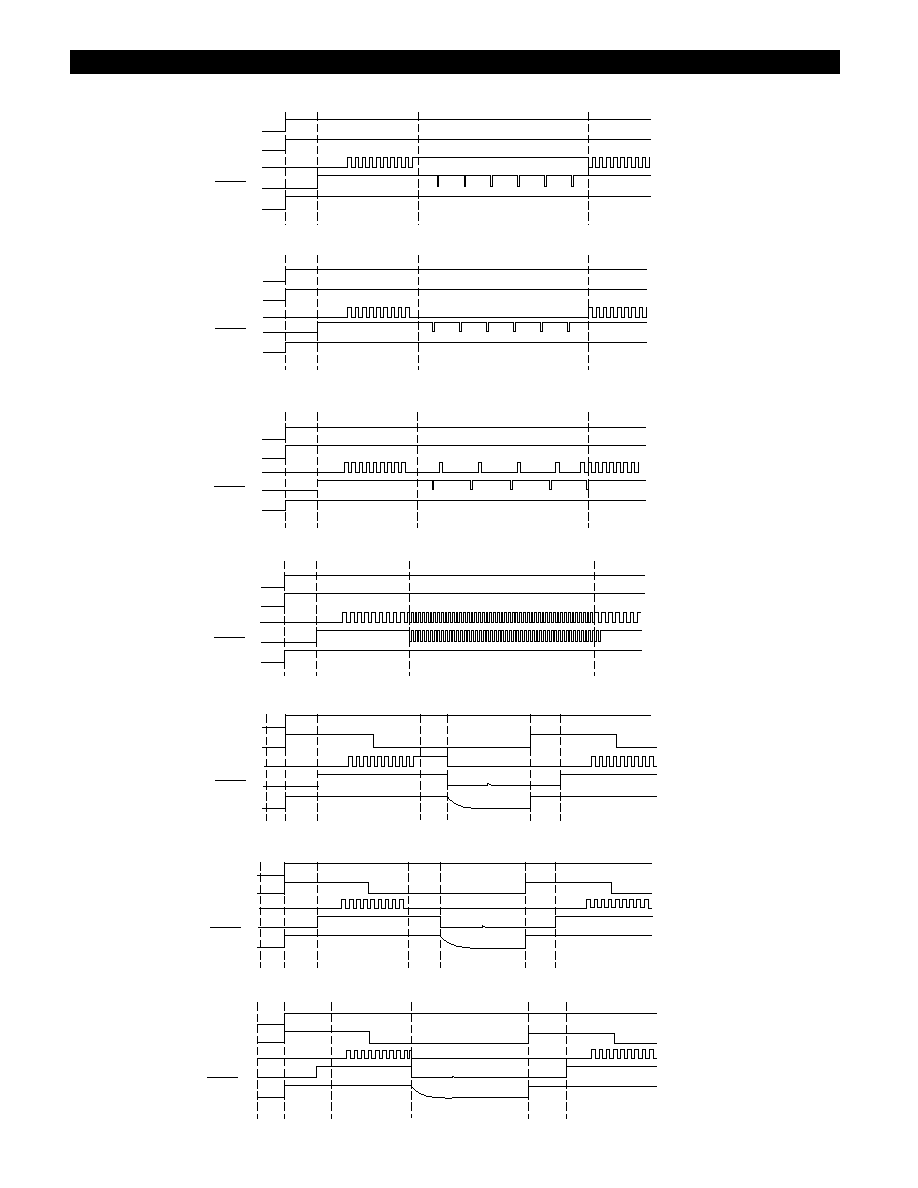
Normal Operation
WDI held High
Figure 3: Timing Diagrams for Watchdog and ENABLE Functions
3a: V
OUT
when Watchdog is held high and ENABLE = HIGH.
Battery
Battery
V
IN
WDI
RESET
V
OUT 0V
0V
0V
POR
Normal Operation
WDI held Low
ENABLE
3b: V
OUT
when Watchdog is held low and ENABLE = HIGH.
Battery
Battery
V
IN
WDI
RESET
V
OUT 0V
0V
0V
POR
Normal Operation
Slow WDI signal
ENABLE
3c: V
OUT
when Watchdog is too slow and ENABLE = HIGH.
Battery
Battery
V
IN
WDI
RESET
V
OUT 0V
0V
0V
POR
Normal Operation
Fast WDI signal
ENABLE
3d: V
OUT
when Watchdog is too fast and ENABLE = HIGH.
Battery
Battery
V
IN
WDI
RESET
V
OUT 0V
0V
0V
POR
Normal Operation
Sleep Mode
WDI
high
POR
Normal Operation
ENABLE
3e: WDI held high after a normal period of operation; ENABLE = LOW.
Battery
Battery
V
IN
WDI
RESET
V
OUT 0V
0V
0V
POR
Normal Operation
Sleep Mode
WDI
low
POR
Normal Operation
ENABLE
3f: WDI held low or is too slow after a normal period of operation; ENABLE = LOW.
Battery
Battery
V
IN
WDI
RESET
V
OUT 0V
0V
0V
POR
Normal Operation
Sleep Mode
POR
Normal Operation
ENABLE
3g: WDI frequency rises above the upper frequency threshold after a normal period of operation; ENABLE = LOW
(for the CS8140 only).
CS8140/1
8
CS8140/1
As long as ENABLE is high or ENABLE is low and the
Watchdog signal is normal, V
OUT
will be at 5V (typ). If
ENABLE is low and the Watchdog signal moves outside
programmable limits, the output transistor turns off and
the IC goes into SLEEP mode. Only the ENABLE circuitry
in the IC remains powered up, drawing a quiescent cur-
rent of 250µA.
The Watchdog monitors the frequency of an incoming
WDI signal. If the signal falls outside of the WDI window,
a frequency programmable pulse train is generated at the
lead (Figure 3) until the correct Watchdog input
signal reappears at the lead (ENABLE = HIGH).
The lower and upper window threshold limits of the
watchdog function are set by the value of C
DELAY
. The lim-
its are determined according to the following equations for
the CS8140:
(a)
t
WDILOWER
= (1.3 x 10
5
)C
DELAY
or
f
WDI(LOWER)
= (7.69 x 10
-6
)C
DELAY
-1
(b)
t
WDI(UPPER)
= (3.82 x 10
-4
)C
DELAY
or
f
WDI(UPPER)
= (2.62 x 10
-5
)C
DELAY
-1
For the CS8141 the lower limit is determined by the equa-
tions in (a) above.
The capacitor C
DELAY
also determines the frequency of the
signal and the POWER-ON-
(POR) delay
period.
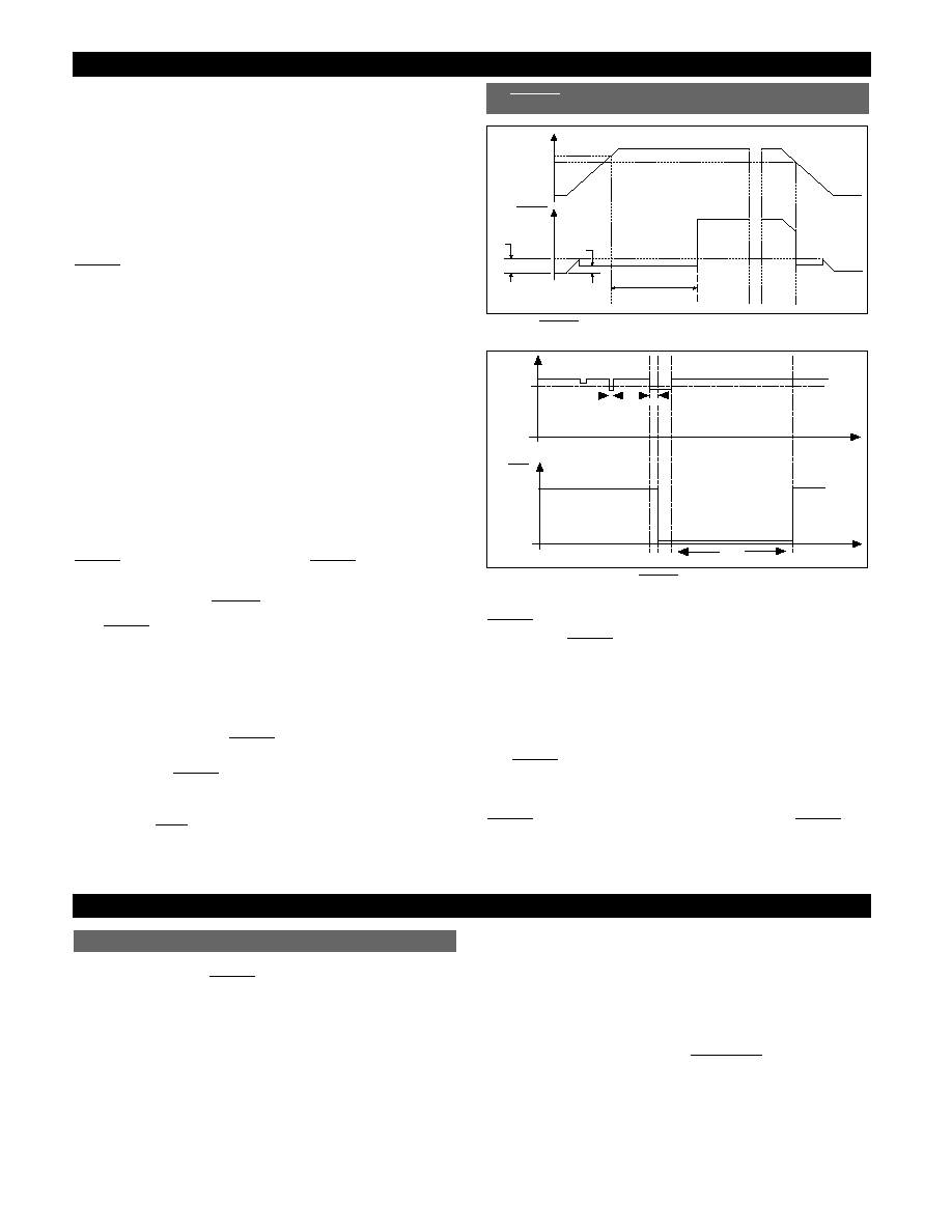
Function
The
function is activated when the Watchdog sig-
nal is outside of its preset window (Figure 3), when the
regulator is in its power up state (Figure 4a) or when V
OUT
drops below V
OUT
-4.5% for more than 2µs (Figure 4b.)
If the Watchdog signal falls outside of the preset voltage
and frequency window, a frequency programmable pulse
train is generated at the
lead (Figure 3) until the
correct Watchdog input signal reappears at the lead. The
duration of the
pulse is determined by C
DELAY
according to the following equation:
t
WDI(
)
= (1 x10
4
)C
DELAY
4a: Power
and Power Down
4b: Undervoltage Triggered
If an undervoltage condition exists, the voltage on the
lead goes low and the delay capacitor, C
DELAY
, is
discharged.
remains low until output is in regula-
tion, the voltage on C
DELAY
exceeds the upper switching
threshold and the Watchdog input signal is within its set
window limits (Figure 4). The delay after the output is in
regulation is:
t
POR(typ)
= (4.75 x 10
5
) C
DELAY
The
delay circuit is also programmed with the
external cap C
DELAY
.
The output of the reset circuit is an open collector NPN.
is operational down to V
OUT
= 1V. Both
and
its delay are governed by comparators with hysteresis to
avoid undesirable oscillations.
RESET
RESET
RESET
RESET
RESET
RESET
V
OUT
V
OUT
-4.5%
<2
mS
RESET
5V
t
POR
≥2ms
RESET
V
OUT
V
R
HI
V
R
LO
V
R
LO
t
POR
RESET
V
R
PEAK
RESET Circuit Waveforms with Delays Indicated
RESET
RESET
RESET
RESET
RESET
RESET
RESET
RESET
Circuit Description: continued
Application Notes
The CS8140 with its unique integration of linear regulator
and control features:
, ENABLE and WATCHDOG,
provides a single IC solution for a microprocessor power
supply. The reset delay, reset duration and watchdog fre-
quency limits are all determined by a single capacitor. For
a particular microprocessor the overriding requirement is
usually the reset delay (also known as power on reset).
The capacitor is chosen to meet this requirement and the
reset duration and watchdog frequency follow.
The reset delay is given by:
t
POR(typ)
= (4.75 x 10
5
)C
DELAY
Assume that the reset delay must be 200ms minimum.
From the CS8140 data sheet the reset delay has a ±37% tol-
erance due to the regulator.
Assume the capacitor tolerance is ±10%.
t
POR
(min) = (4.75 x 10
5
x 0.63) x C
DELAY
x 0.9
C
DELAY
(min) =
C
DELAY
= (min) = 0.743 µF
Closest standard value is 0.82µF.
Minimum and maximum delays using 0.82µF are 220ms
and 586ms.
t
POR
(min)
2.69 x 10
5
RESET
CS8140 Design Example
9
Application Notes
The duration of the reset pulse is given by:
T
WDI(
)
(typ) = (1 x 10
4
) x C
DELAY
This has a tolerance of ±50% due to the IC, and ±10% due
to the capacitor.
The duration of the reset pulse ranges from 3.69ms to
13.5ms.
The watchdog signal can be expressed as a frequency or
time. From a programmers point of view, time is more
useful since they must ensure that a watchdog signal is
issued consistently several times per second.
The maximum and minimum watchdog times are given
by:
t
WDI(LOWER)
= (1.3 x 10
5
)C
DELAY
t
WDI(UPPER)
= (3.82 x 10
4
)C
DELAY
There is a tolerance of ±20% due to the CS8140.
With a capacitor tolerance of ±10%:
t
WDI(LOWER)
= (1.3 x 10
5
) x 1.20 x 1.1 x C
DELAY
t
WDI(UPPER)
= (3.82 x 10
4
) x 0.8 x 0.9 x C
DELAY
t
WDI(LOWER)
= 141ms(max)
t
WDI(UPPER)
= 22.5ms (max)
t
WDI(LOWER)
= (1.3 x 10
5
) x 0.8 x 0.9 x C
DELAY
t
WDI(UPPER)
= (3.82 x 10
4
) x 1.2 x 1.1 x C
DELAY
t
WDI(LOWER)
= 76ms(min)
t
WDI(UPPER)
= 41ms (min)
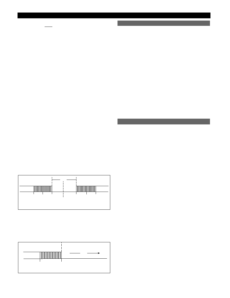
The software must be written so that a watchdog signal
arrives at least every 76ms but not faster than every 41ms
(Figure 5).
Figure 5: WDI signal for CDelay = 0.82µF using CS8140.
The CS8141 is identical to the CS8140 except that the
CS8141 only has a lower watchdog frequency threshold.
The designer using this part need only be concerned with
t
WDI(LOWER)
as shown in Figure 6.
Figure 6: WDI signal for CDelay = 0.82µF using CS8141.
Energy conservation is another benefit of using a regulator
with integrated microprocessor control features. Using the
CS8140 or CS8141 as indicated in Figure 8, the micropro-
cessor can control its own power down sequence. The
momentary contact switch quickly charges C1 through R1.
When the voltage across C1 reaches 3.95V ( the enable
threshold), the output switches on and V
OUT
rises to 5V.
After a delay period determined by C
Delay
, a frequency
programmable reset pulse train is generated at the reset
output. The pulse train continues until the correct watch-
dog signal appears at the WDI lead. C1 is now left to dis-
charge through the input impedance of the enable lead
(approximately 150kΩ) and the enable signal disappears.
The output voltage remains at 5V as long as the CS8140
continues to receive the correct watchdog signal.
The microprocessor can power itself down by terminating
its watchdog signal. When the microprocessor finishes its
housekeeping or power down software routine, it stops
sending a watchdog signal. In response, the regulator
generates a reset signal and goes into a sleep mode where
V
OUT
drops to 0V, shutting down the microprocessor.
The output or compensation capacitor C
2
in Figure 7 helps
determine three main characteristics of a linear regulator:
start-up delay, load transient response and loop stability.
The capacitor value and type should be based on cost,
availability, size and temperature constraints. A tantalum
or aluminum electrolytic capacitor is best, since a film or
ceramic capacitor with almost zero ESR can cause instabili-
ty. The aluminum electrolytic capacitor is the least expen-
sive solution, but, if the circuit operates at low tempera-
tures (-25°C to -40°C), both the value and ESR of the
capacitor will vary considerably. The capacitor manufac-
turers data sheet usually provide this information.
The value for the output capacitor C
2
in Figure 7 should
work for most applications, however it is not necessarily
the optimized solution.
To determine an acceptable value for C
2
for a particular
application, start with a tantalum capacitor of the recom-
mended value and work towards a less expensive alterna-
tive part.
Step 1:
Place the completed circuit with a tantalum capac-
itor of the recommended value in an environmental cham-
ber at the lowest specified operating temperature and
monitor the outputs with an oscilloscope. A decade box
connected in series with the capacitor will simulate the
higher ESR of an aluminum capacitor. Leave the decade
box outside the chamber, the small resistance added by the
longer leads is negligible.
Step 2:
With the input voltage at its maximum value,
increase the load current slowly from zero to full load
while observing the output for any oscillations. If no oscil-
lations are observed, the capacitor is large enough to
ensure a stable design under steady state conditions.
Stability Considerations
Energy Conservation and Smart Features
PASS
FAIL
Hz
ms
7
141
13
76
PASS
FAIL
FAIL
Hz
ms
C = 0.1
mF ± 10%
13
7
44
22.5
9
32
24
41
141
76
31
107
RESET
CS8140/1
10
CS8140/1
Battery
C
1
*
0.1
mF
(optional)
Ignition
0.1
mF
V
IN
V
OUT
ENABLE
DELAY
Gnd
WDI
C
2
**
10
mF*
2.7k
W
RESET
RESET
V
cc
WATCHDOG
PORT
MICROPROCESSOR
5V
CS8140
R***
Application Diagrams
C1
0.1
mF
V
IN
V
OUT
ENABLE
Gnd
WDI
RESET
CS8140/1
C
Delay
R
1
110K
RESET
V
cc
WATCHDOG PORT
MICROPROCESSOR
C2
0.1
mF
2.7k
10
mF
9V
Switch
Figure 8. Applications diagram for CS8140. The CS8140 provides a 5V tightly regulated supply and control function to the microprocessor. In this
application, the microprocessor controls its own power down sequence (see text).
*C1 is required if regulator is located far from the power source filter.
**C2 required for stability
***R ≤ 80kΩ
Figure 7. Application Diagram
11
Application Notes: continued
Step 3:
Increase the ESR of the capacitor from zero using
the decade box and vary the load current until oscillations
appear. Record the values of load current and ESR that
cause the greatest oscillation. This represents the worst
case load conditions for the regulator at low temperature.
Step 4
: Maintain the worst case load conditions set in step
3 and vary the input voltage until the oscillations increase.
This point represents the worst case input voltage condi-
tions.
Step 5:
If the capacitor is adequate, repeat steps 3 and 4
with the next smaller valued capacitor. A smaller capacitor
will usually cost less and occupy less board space. If the
output oscillates within the range of expected operating
conditions, repeat steps 3 and 4 with the next larger stan-
dard capacitor value.
Step 6:
Test the load transient response by switching in
various loads at several frequencies to simulate its real
working environment. Vary the ESR to reduce ringing.
Step 7:
Remove the unit from the environmental chamber
and heat the IC with a heat gun. Vary the load current as
instructed in step 5 to test for any oscillations.
Once the minimum capacitor value with the maximum
ESR is found, a safety factor should be added to allow for
the tolerance of the capacitor and any variations in regula-
tor performance. Most good quality aluminum electrolytic
capacitors have a tolerance of +/- 20% so the minimum
value found should be increased by at least 50% to allow
for this tolerance plus the variation which will occur at
low temperatures. The ESR of the capacitor should be less
than 50% of the maximum allowable ESR found in step 3
above.
The maximum power dissipation for a single output regu-
lator (Figure 9) is:
P
D(max)
=
{
V
IN(max)
- V
OUT(min)
}
I
OUT(max)
+ V
IN(max)
I
Q
(1)
where:
V
IN(max)
is the maximum input voltage,
V
OUT(min)
is the minimum output voltage,
I
OUT(max)
is the maximum output current for the applica-
tion, and
I
Q
is the quiescent current the regulator consumes at
I
OUT(max)
.
Figure 9: Single output regulator with key performance parameters
labeled.
Once the value of P
D(max)
is known, the maximum permis-
sible value of R
QJA
can be calculated:
R
QJA
=
(2)
The value of R
QJA
can then be compared with those in
the package section of the data sheet. Those packages
with R
QJA
's less than the calculated value in equation 2 will
keep the die temperature below 150°C.
In some cases, none of the packages will be sufficient to
dissipate the heat generated by the IC, and an external
heatsink will be required.
A heatsink effectively increases the surface area of the
package to improve the flow of heat away from the IC and
into the surrounding air.
Each material in the heat flow path between the IC and the
outside environment will have a thermal resistance. Like
series electrical resistances, these resistances are summed
to determine the value of R
QJA
:
R
QJA
= R
QJC
+ R
QCS
+ R
QSA
(3)
where:
R
QJC
= the junction–to–case thermal resistance,
R
QCS
= the case–to–heatsink thermal resistance, and
R
QSA
= the heatsink–to–ambient thermal resistance.
R
QJC
appears in the package section of the data sheet. Like
R
QJA
, it too is a function of package type. R
QCS
and R
QSA
are functions of the package type, heatsink and the inter-
face between them. These values appear in heatsink data
sheets of heatsink manufacturers.
Heatsinks
150°C - T
A
P
D
V
IN
Smart
Regulator
V
OUT
I
OUT
I
IN
I
Q
Control
Features
}
Calculating Power Dissipation
in a Single Output Linear Regulator
CS8140/1
12
D
Lead Count
Metric
English
Max
Min
Max
Min
24 Lead SOIC Wide
15.60
15.20
.614
.598
14 Lead PDIP
19.69
18.67
.775
.735
Package Specification
PACKAGE DIMENSIONS IN mm (INCHES)
Ordering Information
PACKAGE THERMAL DATA
Thermal
7 L
24L
24L (Fused) 14 L
Data
TO-220
CS8140
CS8141
PDIP
R
QJC
typ
1.6
16
9
48
˚C/W
R
QJA
typ
50
80
55
85
˚C/W
Rev. 2/23/99
CS8140/1
Part Number
Description
CS8140YT7
7L TO-220 Straight
CS8140YTVA7
7L TO-220 Vertical
CS8140YTHA7
7L TO-220 Horizontal
CS8140YDW24
24L SO
CS8140YDWR24
24L SO (tape & reel)
CS8140YN14
14L PDIP
CS8141YT7
7L TO-220 Straight
CS8141YTVA7
7L TO-220 Vertical
CS8141YTHA7
7L TO-220 Horizontal
CS8141YDWF24
24L SO (internally fused leads)
CS8141YDWFR24
24L SO (internally fused leads)
(tape & reel)
CS8141YN14
14L PDIP
© 1999 Cherry Semiconductor Corporation
Cherry Semiconductor Corporation reserves the
right to make changes to the specifications without
notice. Please contact Cherry Semiconductor
Corporation for the latest available information.
Surface Mount Wide Body (DW); 300 mil wide
1.27 (.050) BSC
7.60 (.299)
7.40 (.291)
10.65 (.419)
10.00 (.394)
D
0.32 (.013)
0.23 (.009)
1.27 (.050)
0.40 (.016)
REF: JEDEC MS-013
2.49 (.098)
2.24 (.088)
0.51 (.020)
0.33 (.013)
2.65 (.104)
2.35 (.093)
0.30 (.012)
0.10 (.004)
Plastic DIP (N); 300 mil wide
0.39 (.015)
MIN.
2.54 (.100) BSC
1.77 (.070)
1.14 (.045)
D
Some 8 and 16 lead
packages may have
1/2 lead at the end
of the package.
All specs are the same.
.203 (.008)
.356 (.014)
REF: JEDEC MS-001
3.68 (.145)
2.92 (.115)
8.26 (.325)
7.62 (.300)
7.11 (.280)
6.10 (.240)
.356 (.014)
.558 (.022)
7 Lead TO-220 (T) Straight
2.87 (.113)
2.62 (.103)
9.78 (.385)
10.54 (.415)
1.40 (.055)
1.14 (.045)
0.64 (.025)
0.38 (.015)
0.56 (.022)
0.36 (.014)
1.40 (.055)
1.14 (.045)
4.83 (.190)
4.06 (.160)
14.22 (.560)
13.72 (.540)
0.94 (.037)
0.58 (.023)
7.75 (.305)
7.49 (.295)
2.92 (.115)
2.29 (.090)
3.71 (.146)
3.96 (.156)
14.99 (.590)
14.22 (.560)
6.55 (.258)
5.94 (.234)
7 Lead TO-220 (TVA) Vertical
10.54 (.415)
9.78 (.385)
2.03 (.080)
7.52 (.296)
4.34
(.171)
1.40 (.055)
1.14 (.045)
14.99 (.590)
14.22 (.560)
11.86 (.467)
4.83 (.190)
4.06 (.160)
8.26
(.325)
7.62 (.300)
0.81
(.030)
1.27
(.050)
TYP
0.56 (.022)
0.36 (.014)
2.92 (.115)
2.29 (.090)
2.87 (.113)
2.62 (.103)
6.55 (.258)
5.94 (.234)
2.92
(.115)
3.96 (.156)
3.71 (.146)