s
Two Regulated Outputs
10V ± 5%; 500 mA
5V ± 3%; 70 mA
s
70µA SLEEP Mode Current
s
Inherently Stable
Secondary Output
(No Output Capacitor
Required)
s
Fault Protection
Overvoltage Shutdown
Reverse Battery
60V Peak Transient
-50V Reverse Transient
Short Circuit
Thermal Shutdown
s
CMOS Compatible
Input with Low
(I
OUT(max)
) Input Current.
ENABLE
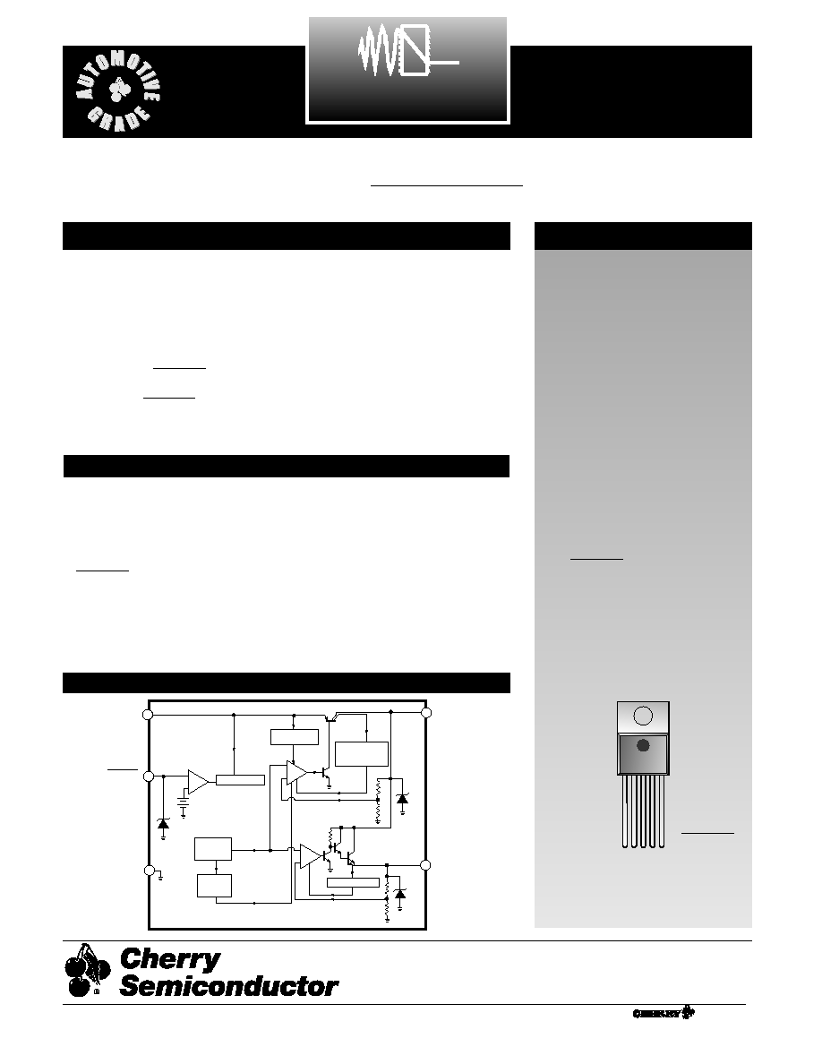
1
Features
Package Options
5 Lead TO-220
Tab (Gnd)
1
CS8147
10V/5V
Low Dropout Dual Regulator
with ENABLE
CS8147
Description
V
IN
V
OUT
2
Gnd
V
OUT
1
ENABLE
Bandgap
Reference
Thermal
Shutdown
Anti-saturation
and
Current Limit
+
-
Current Limit
+
-
+
-
Pre-Regulator
Over Voltage
Shutdown
Secondary Output
Primary Output
Block Diagram
Absolute Maximum Ratings
Input Voltage (V
IN
)
DC .............................................................................................-18V to 26V
Positive Peak Transient Voltage
(46V Load Dump @ V
IN
= 14V) .......................................................60V
Negative Peak Transient Voltage ......................................................-50V
ESD (Human Body Model) ...........................................................................2kV
Input ...................................................................................-0.3 to 10V
Internal Power Dissipation ..................................................Internally Limited
Junction Temperature Range...................................................-40°C to +150°C
Storage Temperature Range ....................................................-65°C to +150°C
Lead Temperature Soldering
Wave Solder (through hole styles only)..........10 sec. max, 260°C peak
ENABLE
The CS8147 is a 10V/5V dual out-
put linear regulator. The 10V ±.5%
output sources 500mA and the 5V
±3% output sources 70mA. The
secondary output is inherently sta-
ble and does not require an external
capacitor.
The on board
function
controls the regulator’s two out-
puts. When
is high, the
regulator is placed in SLEEP mode.
Both outputs are disabled and the
regulator draws only 70µA of qui-
escent current.
The regulator is protected against
overvoltage conditions. Both out-
puts are protected against short
circuit and thermal runaway
conditions.
The CS8147 is packaged in a 5 lead
TO-220 with copper tab. The cop-
per tab can be connected to a heat
sink if necessary.
ENABLE
ENABLE
1
2 V
IN
3 Gnd
4 V
OUT1
(10V)
5 V
OUT2
(5V)
ENABLE
A Company
®
Rev. 4/5/99
Cherry Semiconductor Corporation
2000 South County Trail, East Greenwich, RI 02818
Tel: (401)885-3600 Fax: (401)885-5786
Email: info@cherry-semi.com
Web Site: www.cherry-semi.com
2
CS8147
PARAMETER
TEST CONDITIONS
MIN
TYP
MAX
UNIT
Electrical Characteristics for V
OUT
: V
IN
= 14V, I
OUT1
= I
OUT2
= 5mA, -40°C < T
J
< 150°C, -40°C ≤ T
A
≤ 125˚C,
= LOW; unless otherwise specified.
ENABLE
Package Lead Description
PACKAGE LEAD #
LEAD SYMBOL
FUNCTION
5 Lead TO-220
1
CMOS compatible input lead; switches V
OUT1
and V
OUT2
on
and off. When
is low, V
OUT1
and V
OUT2
are active.
2
V
IN
Supply voltage, usually direct from battery.
3
Gnd
Ground connection.
4
V
OUT1
Regulated output 10V, 500mA (typ)
5
V
OUT2
Secondary output 5V, 70mA (typ).
ENABLE
ENABLE
s Primary Output (V
OUT1
)
Output Voltage
13V ≤ V
IN
≤ 26V, I
OUT1
≤ 500mA,
9.50
10.00
10.50
V
Dropout Voltage
I
OUT1
= 500mA
0.5
0.7
V
Line Regulation
11V ≤ V
IN
≤ 18V, I
OUT1
= 250mA
45
90
mV
Load Regulation
5mA ≤ I
OUT1
≤ 500mA
15
75
mV
Quiescent Current
I
OUT1
≤ 1mA, No Load on V
OUT2
, V
IN
= 18V
3
7
mA
I
OUT1
= 500mA, No Load on V
OUT2
, V
IN
= 11V
60
120
mA
Quiescent Current
= HIGH
70
200
µA
V
OUT1
,V
OUT2
= OFF
Current Limit
0.55
0.80
A
Long Term Stability
50
mV/khr
Over Voltage Shutdown
V
OUT1
and V
OUT2
32
36
40
V
s Secondary Output (V
OUT2
)
Output Voltage
6V ≤ V
IN
≤ 26V, 1mA ≤ I
OUT2
≤ 70mA
4.85
5.00
5.15
V
Dropout Voltage
I
OUT2
≤ 70mA
1.5
2.5
V
Line Regulation
11 ≤ V
IN
≤ 18V, I
OUT
= 70µA
4
50
mV
Load Regulation
1mA ≤ I
OUT2
≤ 70mA, V
IN
= 14V
10
50
mV
Current Limit
150
mA
s
Function (
)
Input
Threshold
V
OUT2(ON)
1.40
2.50
V
V
OUT1(OFF)
.8
1.40
V
Input
Current
Input Voltage Range 0 to 5V
-10
10
µA
ENABLE
ENABLE
ENABLE
ENABLE
ENABLE
3
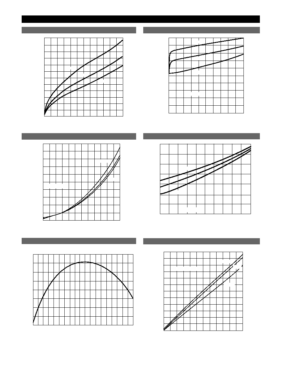
Typical Performance Characteristics
Output Current (mA)
Dropout V
oltage (mV), V
OUT
1
0
50 100 150 200
300 350 400 450 500 550 600
250
0
50
100
150
200
250
300
350
400
450
500
550
600
125
∞C
25
∞C
-40
∞C
Dropout Voltage vs. Output Current (V
OUT1
)
Output Current (mA) V
OUT2 (5V)
Dropout V
oltage (V), V
OUT
2
0
10
0
0.20
125
∞C
25
∞C
-40
∞C
20
30
40
50
60
70
80
90
100
0.40
0.60
0.80
1.00
1.20
1.40
1.60
1.80
2.00
V
IN
= 6.00V
Output Current (mA)
Quiescent Current (mA)
0
50 100 150 200
300 350 400 450 500 550 600
250
0
10
100
20
30
40
50
60
70
80
90
125
∞C
25
∞C
-40
∞C
V
IN
= 14V
Output Current (mA), V
OUT2
(5V)
Quiescent Current (mA)
0
10
0
1
125
∞C
25
∞C
-40
∞C
20
30
40
50
60
70
80
90
100
2
3
4
5
6
7
V
IN
= 14V
Quiescent Current vs. Output Current (V
OUT2
)
Quiescent Current vs. Output Current (V
OUT1
)
Dropout Voltage vs. Output Current (V
OUT2
)
Temp (C
∞)
PART1 V
IN
=14V, RLOAD=0
V
OUT
(V
olts)
-50
4.98
4.99
5.00
5.01
5.02
-40 -30 -20 -10 0 10 20 30 40 50 60
80 90 100 110 120 130
70
140
Output Current (mA), V
OUT1
(10V)
Line Regulation (mV)
0
50 100 150 200
300 350 400 450 500 550 600
250
0
10
100
20
30
40
50
60
70
80
90
-40
∞C
110
120
125
∞C
V
IN
= 11V - 26V
25
∞C
Line Regulation vs. Output Current (V
OUT1
)
V
OUT2
vs. Temperature
CS8147
4
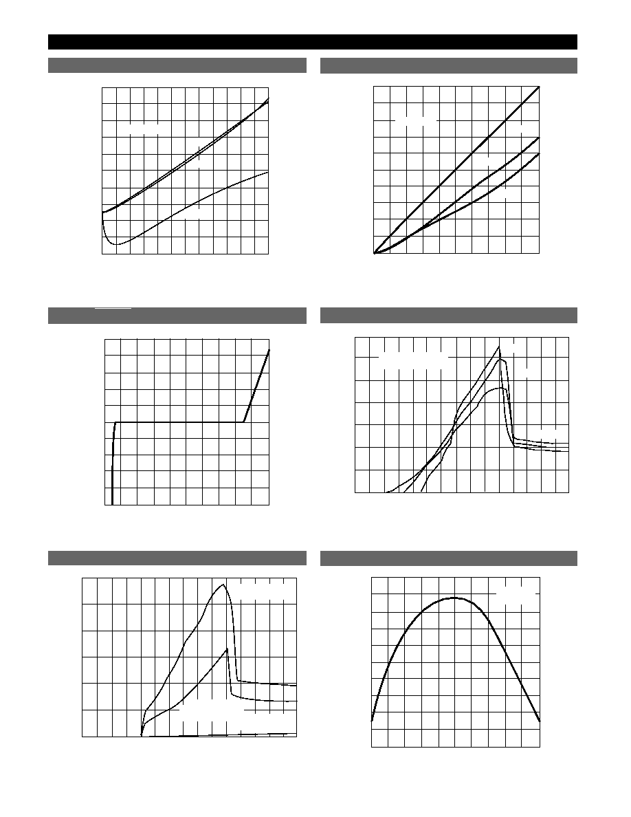
Typical Performance Characteristics
Output Current (mA), V
OUT1
(10V)
Load Regulation (mV)
0
50 100 150 200
300 350 400 450 500 550 600
250
-10
-6
22
-2
2
6
10
14
18
125
∞C
25
∞C
-40
∞C
26
30
V
IN
= 14V
Load Regulation vs. Output Current (V
OUT1
)
Output Current (mA), V
OUT2
(5V)
Load Regulation (mV)
0
10
0
1
20
30
40
50
60
70
80
90
100
2
3
8
4
5
6
7
9
10
V
IN
= 14V
-40
∞C
25
∞C
125
∞C
Load Regulation vs. Output Current (V
OUT2
)
V
ENABLE
1.000/div (V)
I
ENABLE
(
m
A)
-1.000
0
-100.0
9.000
20.00
/div
0
100.0
ENABLE Input Current vs. Input Voltage
-40˚C
25˚C
V10 = 500mA Load
V5 = 70mA Load
350
300
250
200
150
100
50
0
0
1
2
3
4
5
6
7
8
9 10 11 12 13 14 15
V
IN
(V)
ICQ
(mA)
125˚C
0 1 2
3 4
5 6
7
8
9 10 11 12 13 14 15
0
50
100
150
200
250
300
ICQ (mA)
V
IN
(V)
V
OUT1
= 500mA Load
V
OUT2
= 100mA Load
V10 = 500mA Load
V5 = No Load
V
OUT1
= No Load
V
OUT2
= No Load
Quiescent Current (I
CQ
) vs. V
IN
over R
LOAD
TEMP (
∞C)
V
OUT
(V)
-50 -30
9.975
9.980
-10
10
30
50
70
90
110 130 150
9.985
9.990
9.995
10.000
10.005
10.010
10.015
10.020
10.025
V
IN
= 14V
I
O
= 30mA
V
OUT1
vs. Temperature
Quiescent Current (I
CQ
) vs. V
IN
over Temperature
CS8147
5
Definition of Terms
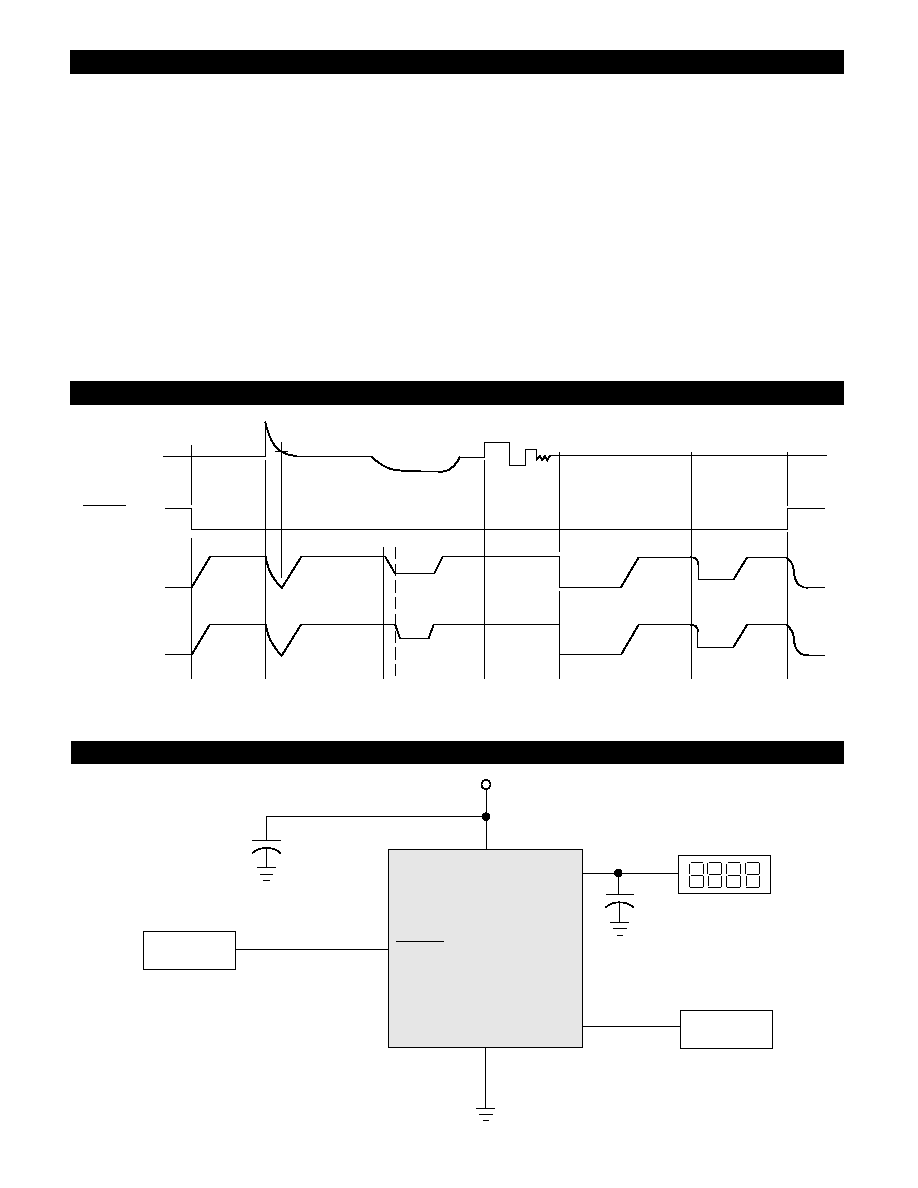
Typical Circuit Waveform
Test & Applications Circuit
Dropout Voltage:
The input-output voltage differential at which
the circuit ceases to regulate against further reduction
in input voltage. Measured when the output voltage
has dropped 100mV from the nominal value obtained
at 14V input, dropout voltage is dependent upon load
current and junction temperature.
Current Limit:
Peak current that can be delivered to the output.
Input Voltage:
The DC voltage applied to the input terminals
with respect to ground.
Input Output Differential:
The voltage difference between the
unregulated input voltage and the regulated output
voltage for which the regulator will operate.
Line Regulation:
The change in output voltage for a change in
the input voltage. The measurement is made under
conditions of low dissipation or by using pulse tech-
niques such that the average chip temperature is not
significantly affected.
Load Regulation:
The change in output voltage for a change in
load current at constant chip temperature.
Long Term Stability:
Output voltage stability under accelerated
life-test conditions after 1000 hours with maximum
rated voltage and junction temperature.
Output Noise Voltage:
The rms AC voltage at the output, with
constant load and no input ripple, measured over a
specified frequency range.
Quiescent Current:
The part of the positive input current that
does not contribute to the positive load current. The
regulator ground lead current.
Ripple Rejection:
The ratio of the peak-to-peak input ripple
voltage to the peak-to-peak output ripple voltage.
Temperature Stability of V
OUT
:
The percentage change in out-
put voltage for a thermal variation from room tempera-
ture to either temperature extreme.
V
IN
ENABLE
V
OUT1
System
Condition
60V
5V
5V
10V
0V
Turn
On
Load
Dump
Low V
IN
Line Noise, Etc.
V
OUT
Short
Circuit
Thermal
Shutdown
Turn
Off
5V
0V
14V
5V
2.0V
0.8V
14V
26V
31V
10V
10V
10V
10V
0V
V
OUT2
0V
0V
0V
0V
5V
3V
5V
5V
0V
CS8147
C
1
*
0.1
mF
ENABLE
V
IN
V
OUT
1
Gnd
V
OUT
2
C
2
**
10
mF
10V
5V
Control
DISPLAY
Tuner IC
* C
1
is required if the regulator is located away from the power source filter.
**C
2
is required for stability.
CS8147