5V, 100mA Low Dropout Linear Regulator
with WATCHDOG, RESET, & WAKE UP
The CS8151 is a precision 5V, 100mA
micro-power voltage regulator with
very low quiescent current (400µA
typical at 200µA load). The 5V output
is accurate within ±2% and supplies
100 mA of load current with a typical
dropout voltage of 400mV.
Microprocessor control logic includes
Watchdog, Wake Up and
. This
unique combination of low quiescent
current and full microprocessor con-
trol makes the CS8151 ideal for use in
battery operated, microprocessor con-
trolled equipment.
The CS8151 WAKE UP function brings
the microprocessor out of Sleep mode.
The microprocessor in turn, signals its
WAKE UP status back to the CS8151
by issuing a WATCHDOG signal.
The WATCHDOG logic function mon-
itors an input signal (WDI) from the
microprocessor. The CS8151 responds
to the falling edge of the WATCH-
DOG signal which it expects at least
once during each wake-up period.
When the correct WATCHDOG signal
is received, a falling edge is issued on
the wake-up signal line.
is independent of V
IN
and
operates correctly to an output voltage
as low as 1V. A
signal is issued
in any of three situations. During
power up the
is held low until
the output voltage is in regulation.
During operation if the output voltage
shifts below the regulation limits, the
toggles low and remains low
until proper output voltage regulation
is restored. And finally, a
signal
is issued if the regulator does not
receive a WATCHDOG signal within
the WAKE UP period.
The
pulse width, WAKE UP
signal frequency, and WAKE UP delay
time are all set by one external capaci-
tor C
Delay
.
The regulator is protected against
short circuit, over voltage, and thermal
runaway conditions. The device can
withstand 74 volt load dump tran-
sients, making it suitable for use in
automotive environments.
RESET
RESET
RESET
RESET
RESET
RESET
RESET
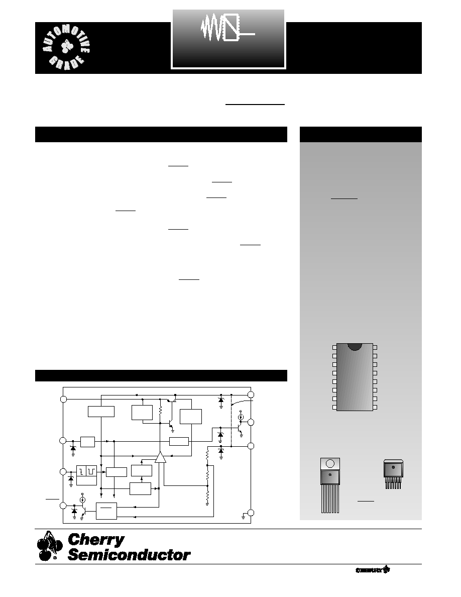
1
Features
Error
Amplifier
Thermal
Shutdown
V
IN
Bandgap
Reference
+ -
Current Limit
Sense
Current Source
(Circuit Bias)
RESET
Over
Voltage
Shutdown
Timing
Circuit
WATCHDOG
Circuit
Falling Edge
Detector
Sense
V
OUT
Gnd
Delay
WDI
RESET
Circuit
VOUT
VOUT
WAKE UP
WAKE UP
Circuit
internally
connected on
TO-220 and
D
2
PAK
s
5V ±2% / 100 mA Output
Voltage
s
Micropower Compatible
Control Functions:
WAKE UP
WATCHDOG
s
Low Dropout Voltage:
400mV @ 100mA
s
Low Sleep Mode Quiescent
Current (400µA typ)
s
Protection Features:
Thermal Shutdown
Short Circuit
74V Load Dump
Reverse Transient (-50V)
RESET
Package Options
16 Lead PDIP
16 Lead SOIC Wide*
(Internally Fused)
CS8151
1
N/C
N/C
N/C
N/C
Gnd
Gnd
Gnd
Gnd
Sense
V
OUT
Delay
______
RESET
WAKE UP
WDI
V
IN
*N/C
* For SO Wide package, pin # 6 is Gnd
CS8151
Description
Block Diagram
7 Lead TO-220
Tab (Gnd)
1
7 Lead D
2
PAK
Tab (Gnd)
1
1. V
OUT
2. V
IN
3. WDI
4. Gnd
5. WAKE UP
6.
7. Delay
RESET
A Company
®
Rev. 5/4/99
Cherry Semiconductor Corporation
2000 South County Trail, East Greenwich, RI 02818
Tel: (401)885-3600 Fax: (401)885-5786
Email: info@cherry-semi.com
Web Site: www.cherry-semi.com
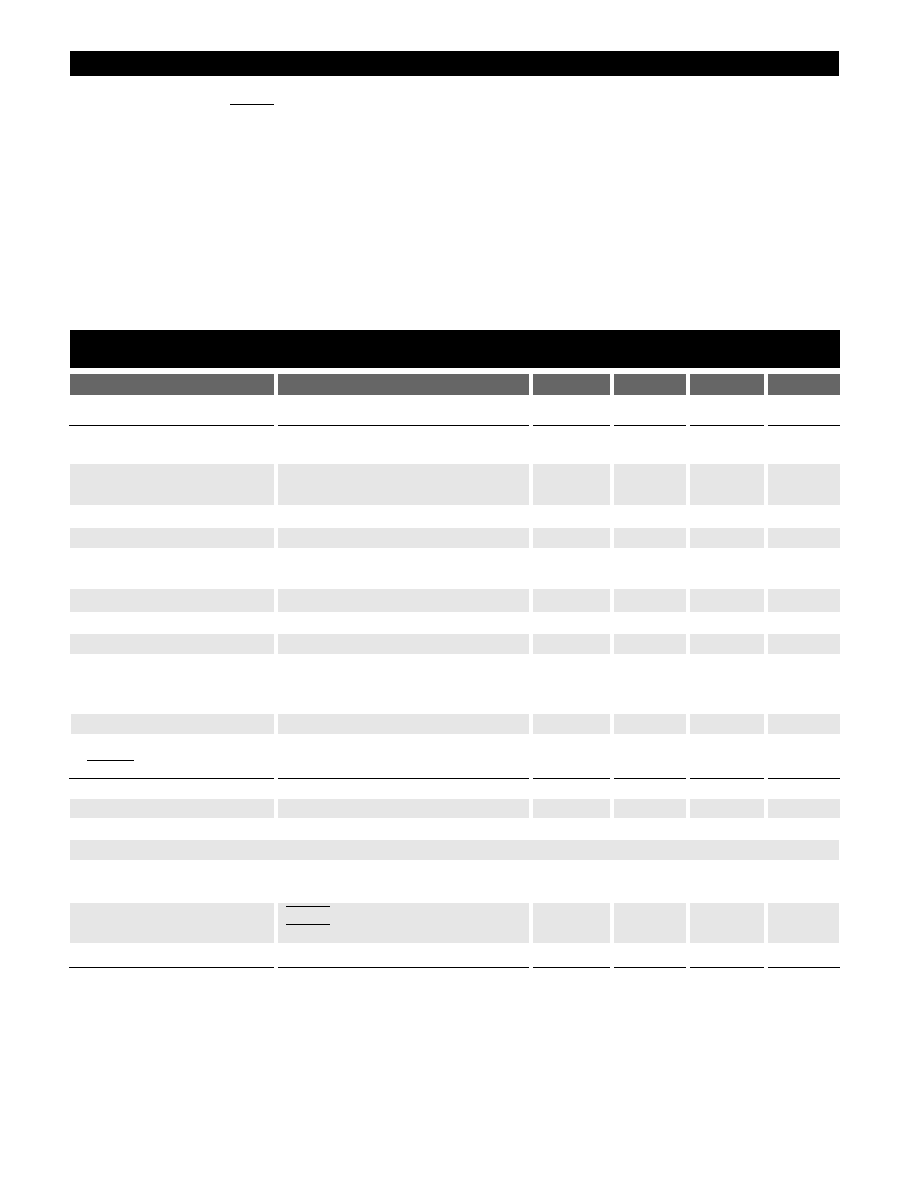
2
PARAMETER
TEST CONDITIONS
MIN
TYP
MAX
UNIT
Absolute Maximum Ratings
Power Dissipation.............................................................................................................................................Internally Limited
Output Current (V
OUT
,
, WAKE UP) .................................................................................................Internally Limited
Reverse Battery..........................................................................................................................................................................-15V
Maximum Load Dump Transient .........................................................................................................................................+74V
Maximum Negative Transient (t<2ms) .................................................................................................................................-50V
ESD Susceptibility (Human Body Model)..............................................................................................................................2kV
ESD Susceptibility (Machine Model).....................................................................................................................................200V
Logic Inputs/Outputs ................................................................................................................................................-0.3V to +6V
Storage Temperature Range ................................................................................................................................-55°C to +150°C
Lead Temperature Soldering
Wave Solder (through hole styles only) .....................................................................................10 sec. max, 260°C peak
Reflow (SMD styles only) ......................................................................................60 sec. max above 183°C, 230°C peak
RESET
CS8151
Electrical Characteristics: T
A
= -40°C to +125°C, -40°C ≤ T
J
≤ 150°C, 6V ≤ V
IN
≤ 26V, I
OUT
= 100µA to 100mA, C
2
= 47µF
(ESR < 8Ω), C
Delay
= 0.1µF (unless otherwise noted)
s Output Section
Output Voltage, V
OUT
9V < V
IN
< 16V
4.90
5.00
5.10
V
6V < V
IN
< 26V, 0 < I
OUT
< 100mA
4.85
5.00
5.15
V
Dropout Voltage (V
IN
- V
OUT
)
I
OUT
= 100mA
400
600
mV
I
OUT
= 100µA
100
150
mV
Load Regulation
V
IN
= 14V, 100µA < I
OUT
< 100mA
10
50
mV
Line Regulation
I
OUT
= 1mA, 6V < V
IN
< 26V
10
50
mV
Ripple Rejection
7V < V
IN
< 17V @ f = 120Hz,
60
75
dB
I
OUT
= 100mA
Current Limit
V
OUT
= 4.5V
100
250
mA
Thermal Shutdown
150
180
210
°C
Overvoltage Shutdown
V
OUT
< 1V
50
56
62
V
Quiescent Current
I
OUT
= 200µA (Sleep)
0.40
0.75
mA
I
OUT
= 50mA
4
mA
I
OUT
= 100mA (WAKE UP)
12
20
mA
Reverse Current
V
OUT
= 5V, V
IN
= 0V
1.0
1.5
mA
s
Threshold High (RTH)
RTH V
OUT
Increasing
V
OUT
- 0.3
V
OUT
- 0.04
V
Threshold Low (RTL)
RTL V
OUT
Decreasing
4.50
4.70
4.91
V
Hysteresis
RTH – RTL
150
200
250
mV
Output
LOW
1V < V
OUT
< RTL, I
OUT
= 25µA
0.2
0.8
V
HIGH
I
OUT
= 25µA, V
OUT
> RTH
3.8
4.2
5.1
V
Current Limit
= 0V, V
OUT
> V
RTH
(sourcing)
0.025
0.50
1.30
mA
= 5V, V
OUT
> 1V (sinking)
0.1
12
80
mA
Delay Time
POR Mode
3
5
7
ms
RESET
RESET
RESET
3
Package Lead Description
Package Lead #
Lead Symbol
Function
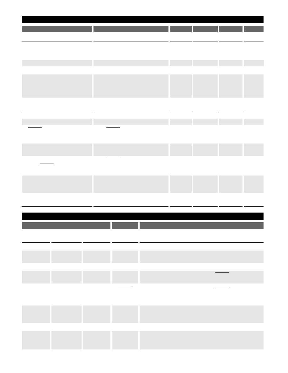
Electrical Characteristics: continued
PARAMETER
TEST CONDITIONS
MIN
TYP
MAX
UNIT
CS8151
s WATCHDOG Input
Threshold
HIGH
1.4
2.0
V
LOW
0.8
1.3
V
Hysteresis
25
100
mV
Input Current
0 < WDI < 6V
-10
0
+10
µA
Pulse Width
50% WDI falling edge to
5
µs
50% WDI rising edge and
50% WDI rising edge to 50%
WDI falling edge (see Figure 1)
s WAKE UP Output
WAKE UP Period
see Figure 1a
30
40
50
ms
WAKE UP Duty Cycle nominal
see Figure 1c
40
50
60
%
HIGH to WAKE UP
50%
rising edge to
15
20
25
ms
Rising Delay Time
50% WAKE UP edge
(see Figure 1)
WAKE UP Response
50% WDI falling edge to
2
10
µs
to Watchdog Input
50% WAKE UP falling edge
WAKE UP Response
50%
falling edge to
2
10
µs
to
50% WAKE UP falling edge
V
OUT
= 5V
Æ4.5V
Output
LOW
I
OUT
= 25µA(sinking)
0.2
0.8
V
HIGH
I
OUT
= 25µA(sourcing)
3.8
4.2
5.1
V
Current Limit
WAKE UP = 5V
0.025
1.00
7.00
mA
WAKE UP = 0V
.05
3.50
mA
RESET
RESET
RESET
RESET
7L TO-220 &
16 L PDIP
16L SOIC
7L D
2
PAK
(internally fused) (internally fused)
2
9
9
V
IN
Supply voltage to the IC.
3
11
11
WDI
CMOS/TTL compatible input lead. The watchdog function
monitors the falling edge of the incoming signal.
4
4,5,12,13
4,5,6,12,13
Gnd
Ground Connection
7
16
16
Delay
Input lead from timing capacitor for
and WAKE UP
signal.
6
15
15
CMOS/TTL compatible output lead
goes low when-
ever V
OUT
drops by more than 6% from nominal, or during
the absence of a correct watchdog signal.
5
14
14
WAKE UP
CMOS/TTL compatible output consisting of a continuously
generated signal used to WAKE UP the microprocessor from
sleep mode.
1
8
8
V
OUT
Regulated output voltage 5V ± 2%.
7
7
Sense
Kelvin connection which allows remote sensing of the output
voltage for improved regulation. If remote sensing is not
required, connect to V
OUT
.
RESET
RESET
RESET
4
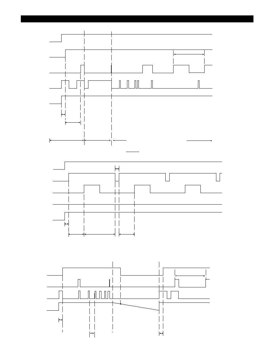
______
RESET
WAKE UP
WDI
V
OUT
POWER DOWN
POR
POR
RTL
WATCHDOG Pulse Width
WAKE UP period
Timing Diagrams
Figure 1c. Power Down and Restart Sequence
______
RESET
WAKE UP
WDI
V
OUT
VIN
POR
______
RESET HIGH
to WAKE UP
DELAY TIME
______
RESET HIGH
to WAKEUP
DELAY TIME
______
RESET delay time
WAKE UP
period
Figure 1b. Error Condition: Watchdog remains LOW and a
is issued
RESET
______
RESET
WAKE UP
WDI
V
OUT
-
POR
V
IN
______
RESET High
to Wakeup
Delay Time
Power Up
Sleep Mode
Normal Operation with varying WATCHDOG Signal
WAKE UP Duty Cycle = 50%
Figure 1a. Power Up, Sleep Mode and Normal Operation
CS8151

5
To reduce the drain on the battery a system can go into a
low current consumption mode when ever its not per-
forming a main routine. The WAKE UP signal is generated
continuously and is used to interrupt a microcontroller
that is in sleep mode. The nominal output is a 5 volt
square wave with a duty cycle of 50% at a frequency that
is determined by a timing capacitor, C
Delay
.
When the microprocessor receives a rising edge from the
WAKE UP output, it must issue a watchdog pulse and
check its inputs to decide if it should resume normal oper-
ations or remain in the sleep mode.
The first falling edge of the watchdog signal causes the
WAKE UP to go low within 2µs (typ) and remain low until
the next WAKE UP cycle (see Figure 2). Other watchdog
pulses received within the same cycle are ignored (Figure
1).
During power up,
is held low until the output volt-
age is in regulation. During operation, if the output volt-
age shifts below the regulation limits, the RESET toggles
low and remains low until proper output voltage regula-
tion is restored. After the
delay,
returns
high.
The WATCHDOG circuitry continuously monitors the
input watchdog signal (WDI) from the microprocessor.
The absence of a falling edge on the WATCHDOG input
during one WAKE UP cycle will cause a
pulse to
occur at the end of the WAKE UP cycle. (see Figure 1b).
The WAKE UP output is pulled low during a
regardless of the cause of the
. After the
returns high, the WAKE UP cycle begins again (see
Figures 1b).
The
pulse width, WAKE UP signal frequency and
high to WAKE UP delay time are all set by one
external capacitor C
Delay
.
WAKE UP period=(4x10
5
)C
Delay
Delay Time=(5x10
4
)C
Delay
HIGH to WAKE UP Delay Time =(2x10
5
)C
Delay
Capacitor temperature coefficient and tolerance as well as the
tolerance of the CS8151 must be taken into account in order
to get the correct system tolerance for each parameter.
Figure 2. WAKE UP response to WDI
Figure 3. WAKE UP response to
(Low Voltage)
RESET
WAKE UP
Response to
______
RESET
______
RESET
WAKE UP
WAKE UP
Response to
WDI
WAKE UP
WDI
RESET
RESET
RESET
RESET
RESET
RESET
RESET
RESET
RESET
RESET
RESET
Dropout Voltage:
The input-output voltage differential at which the cir-
cuit ceases to regulate against further reduction in
input voltage. Measured when the output voltage has
dropped 100mV from the nominal value obtained at
14V input, dropout voltage is dependent upon load
current and junction temperature.
Input Voltage:
The DC voltage applied to the input terminals with
respect to ground.
Line Regulation:
The change in output voltage for a change in the
input voltage. The measurement is made under con-
ditions of low dissipation or by using pulse tech-
niques such that the average chip temperature is not
significantly affected.
Load Regulation:
The change in output voltage for a change in load
current at constant chip temperature.
Quiescent Current:
The part of the positive input current that does not
contribute to the positive load current. The regulator
ground lead current.
Ripple Rejection:
The ratio of the peak-to-peak input ripple voltage to
the peak-to-peak output ripple voltage.
Current Limit:
Peak current that can be delivered to the output.
Definition of Terms
Circuit Description
CS8151
Functional Description