 | –≠–ª–µ–∫—Ç—Ä–æ–Ω–Ω—ã–π –∫–æ–º–ø–æ–Ω–µ–Ω—Ç: CS8161YT5 | –°–∫–∞—á–∞—Ç—å:  PDF PDF  ZIP ZIP |
1
Features
s
Two regulated outputs
12V ±5.0%; 400mA
5V ±2.0%; 200mA
s
Very low SLEEP mode cur-
rent drain 200nA
s
Fault Protection
Reverse Battery (-15V)
74V Load Dump
-100V Reverse Transient
Short Circuit
Thermal Shutdown
Package Options
TO-220 5 Lead
16 Lead SO Wide
(internally fused leads)
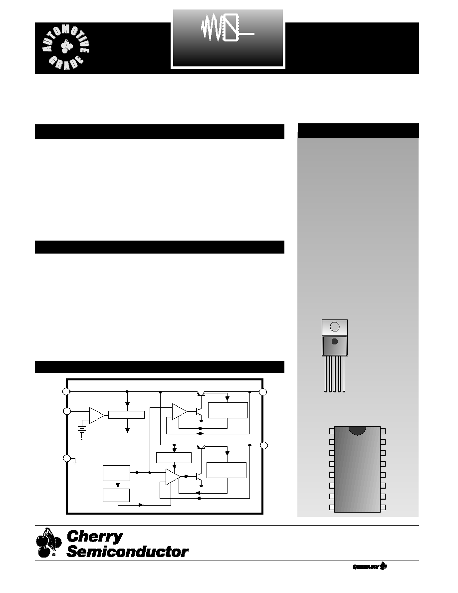
Tab (Gnd)
1
CS8161
CS8161
Description
V
I N
V
O U T
2
Gnd
V
O U T
1
ENABLE
+
-
Bandgap
Reference
+
-
+
-
Thermal
Shutdown
Over Voltage
Shutdown
Anti-saturation
and
Current Limit
Anti-saturation
and
Current Limit
Pre-Regulator
Block Diagram
Absolute Maximum Ratings
Input Voltage
Operating Range .....................................................................–15V to 26V
Overvoltage Protection.........................................................................74V
Internal Power Dissipation ..................................................Internally Limited
Junction Temperature Range.......................................................–40°C +150°C
Storage Temperature Range....................................................–65°C to +150°C
Lead Temperature Soldering
Wave Solder (through hole styles only)..........10 sec. max, 260°C peak
Reflow (SMD styles only)...........60 sec. max above 183°C, 230°C peak
ESD (Human Body Model) ...........................................................................2kV
The CS8161 is a 12V/5V dual out-
put linear regulator. The 12V ± 5%
output sources 400mA and the 5V
±2.0% output sources 200mA.
The on board ENABLE function
controls the regulator’s two out-
puts. When the ENABLE pin is
low, the regulator is placed in
SLEEP mode. Both outputs are dis-
abled and the regulator draws only
200nA of quiescent current.
The primary output, V
OUT1
is pro-
tected against overvoltage condi-
tions. Both outputs are protected
against short circuit and thermal
runaway conditions.
The CS8161 is packaged in a 5 lead
TO–220 with copper tab. The cop-
per tab can be connected to a heat
sink if necessary. It is also available
in a 16 lead SO wide package.
1 V
IN
2 V
OUT1
3 Gnd
4 ENABLE
5 V
OUT2
V
IN
V
OUT(1)
NC
V
OUT(2)
SENSE
1
SENSE
1
NC
NC
NC
Gnd
Gnd
Gnd
Gnd
Gnd
Gnd
ENABLE
1
12V, 5V Low Dropout Dual Regulator
with ENABLE
A Company
®
Rev. 4/5/99
Cherry Semiconductor Corporation
2000 South County Trail, East Greenwich, RI 02818
Tel: (401)885-3600 Fax: (401)885-5786
Email: info@cherry-semi.com
Web Site: www.cherry-semi.com
2
CS8161
PARAMETER
TEST CONDITIONS
MIN
TYP
MAX
UNIT
Electrical Characteristics for V
OUT
: 6V ≤ V
IN
≤ 26V, I
OUT1
= 5mA, I
OUT2
= 5mA, -40°C ≤ T
J
≤ +150˚C,
-40°C ≤ T
A
≤ +125˚C; unless otherwise specified.
s Primary Output Stage(V
OUT1
)
Output Voltage, V
OUT1
13V≤V
IN
≤26V, I
OUT1
≤400mA
11.4
12.0
12.6
V
Dropout Voltage
I
OUT1
=400mA
0.35
0.6
V
Line Regulation
13V≤V
IN
≤20V,5mA≤ I
OUT
<400mA
80
mV
Load Regulation
5mA≤ I
OUT1
≤400mA, V
IN
=14V
80
mV
Quiescent Current
I
OUT1
=100mA, No Load on V
OUT2
8
12
mA
I
OUT1
=400mA, No Load on V
OUT2
50
75
mA
Ripple Rejection
f=120Hz, I
OUT
=300µA, 42
dB
V
IN
=15.0V
DC
, 2V
RMS
Current Limit
0.40
1.0
A
Reverse Polarity
V
OUT1
≥-0.6V, 10Ω Load
-30
-18
V
Input Voltage, DC
Reverse Polarity Input
1% Duty Cycle, t=100ms, V
OUT
≥-6V,
-80
-50
V
Voltage, Transient
10Ω Load
Over-voltage Shutdown
28
34
45
V
Short Circuit Current
700
mA
s Secondary Output (V
OUT2
)
Output Voltage, (V
OUT2
)
6V≤V
IN
≤26V, I
OUT2
≤200mA
4.90
5.10
V
Dropout Voltage
I
OUT2
≤200mA
0.35
0.60
V
Line Regulation
6V≤V
IN
≤26V, 1mA≤I
OUT
≤200mA
50
mV
Load Regulation
1mA≤I
OUT2
≤200mA, 9V
IN
=14V
50
mV
Quiescent Current
I
OUT2
=50mA
5
10
mA
I
OUT2
=200mA
20
35
mA
Ripple Rejection
f=120Hz; I
OUT
=10mA, 42
dB
V
IN
=15V, 2V
RMS
Current Limit
200
600
mA
Short Circuit Current
400
mA
s ENABLE Function (ENABLE)
Input ENABLE Threshold
V
OUT1
Off
1.30
0.80
V
V
OUT1
On
2.00
1.30
V
Input ENABLE Current
V
ENABLE
=5.5V
80
500
µA
V
ENABLE
<0.8V
-10
10
µA
s Other Features
Sleep Mode
V
ENABLE
<0.4V
0.2
50
µA
Thermal Shutdown
150
210
°C
Quiescent Current in Dropout I
OUT1
=100mA, I
OUT2
=50mA
60
mA
3
PACKAGE PIN #
PIN SYMBOL
FUNCTION
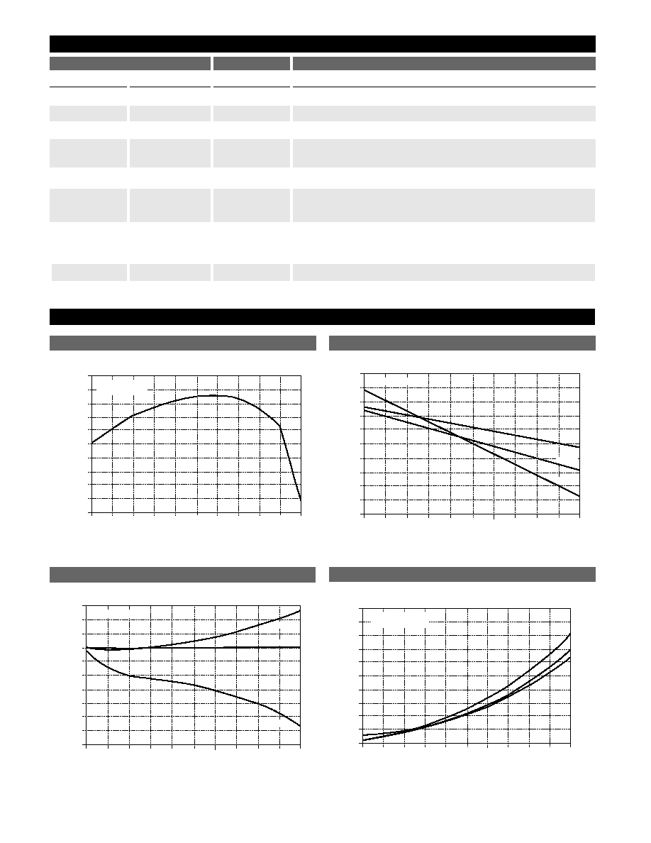
Typical Performance Characteristics
Package Pin Description
CS8161
-40
-20
0
20
40
60
80
100
120
140
160
11.750
11.790
11.830
11.870
11.910
11.950
11.990
12.030
12.070
12.110
12.150
Temperature (Deg. C)
V
olt 1
V
IN
= 14V
I
OUT1
= 5A
Output Voltage vs. Temperature for V
OUT1
0
50
100
150
200
250
300
350
400
450
500
-40
-35
-30
-25
-20
-15
-10
-5
0
5
10
Output Current (mA)
Line Regulation (mV)
-40
∞C
125
∞C
25
∞C
VIN = 13 - 26V
Line Regulation vs. Output Current for V
OUT1
0
50
100
150
200
250
300
350
400
450
500
-40
-35
-30
-20
-15
-10
-5
0
5
10
15
Output Current (mA)
Load Regulation (mV)
VIN = 14.0V
125
∞C
25
∞C
-40
∞C
Load Regulation vs. Output Current for V
OUT1
0
50
100
150
200
250
300
350
400
450
500
0
10
20
30
40
50
60
70
80
90
100
Output Current (mA)
Quiescent Current (mA)
-40
∞C
125
∞C
25
∞C
V
IN
= 14.0V
No Load on V
OUT2
Quiescent Current vs. Output Current for V
OUT1
5 L TO-220
16L SO Wide
1
3
V
IN
Supply voltage, usually direct from battery.
2
6
V
OUT1
Regulated output 12V, 400mA (typ)
3
4,5,12,13,15,16
Gnd
Ground connection.
4
8
ENABLE
CMOS compatible input pin; switches outputs on and off. When
ENABLE is high V
OUT1
and V
OUT2
are active.
5
10
V
OUT2
Output 5V, 200mA (typ).
N/A
7
Sense
1
Kelvin connection that allows remote sensing of V
OUT1
for
improved regulation. If remote sensing is not required, connect
to V
OUT1
.
N/A
11
Sense
2
Kelvin connection that allows remote sensing of V
OUT2
for
improved regulation. If remote sensing is not required, connect
to V
OUT2
.
N/A
1,2,9,14
NC
No Connection
4
CS8161
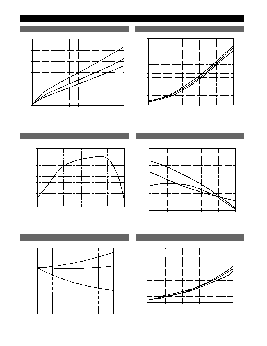
Typical Performance Characteristics: continued
0
400
50
100
500
150
200
250
300
350
450
50
100
150
200
250
300
350
400
450
500
550
600
Output Current (mA)
Dropout V
oltage (mV)
V
IN
= 11V
0
125
∞C
25
∞C
-40
∞C
Dropout Voltage vs. Output Voltage for V
OUT1
0
50
100
150
200
250
300
350
400
450
500
0
10
20
30
40
50
70
80
90
110
150
Output Current (mA)
Quiescent Current (mA)
-40
∞C
125
∞C
25
∞C
V
IN
= 11.0V
No Load on V
OUT2
140
130
120
60
100
Quiescent Current vs Output Current @ Dropout for V
OUT1
-40
-20
0
20
40
60
80
100
120
140
160
4.975
4.980
4.985
4.990
4.995
5.000
5.005
5.010
5.015
5.020
5.025
Temperature (Deg. C)
Output V
oltage
V
IN
= 14V
I
OUT
= 5mA
Output Voltage vs. Temperature for V
OUT2
0
25
50
75
250
100
125
150
175
200
225
-8
-7
-6
-5
-4
-3
-2
-1
0
1
2
3
Output Current (mA)
Load Regulation (mV)
125
∞C
25
∞C
-40
∞C
V
IN
= 6 - 26V
Line Regulation vs Output Current for V
OUT2
0
25
50
75
100
125
150
175
200
225
250
-18
-12
-10
-8
-6
-4
-2
2
4
6
8
Output Current (mA)
Load Regulation (mV)
V
IN
= 14.0V
125
∞C
25
∞C
-40
∞C
0
-14
-16
Load Regulation vs Output Current for V
OUT2
0
25
50
75
100
125
150
175
200
225
250
0
5
10
15
20
25
30
35
40
45
50
Output Current (mA)
Quiescent Current (mA)
-40
∞C
125
∞C
25
∞C
V
IN
= 14.0V
No Load on V
OUT1
Quiescent Current vs Output Current for V
OUT2
5
Definition of Terms
Dropout Voltage:
The input-output voltage differential at
which the circuit ceases to regulate against further
reduction in input voltage. Measured when the
output voltage has dropped 100mV from the nom-
inal value obtained at 14V input, dropout voltage
is dependent upon load current and junction tem-
perature.
Input Voltage:
The DC voltage applied to the input termi-
nals with respect to ground.
Input Output Differential:
The voltage difference
between the unregulated input voltage and the
regulated output voltage for which the regulator
will operate.
Line Regulation:
The change in output voltage for a
change in the input voltage. The measurement is
made under conditions of low dissipation or by
using pulse techniques such that the average chip
temperature is not significantly affected.
Load Regulation:
The change in output voltage for a
change in load current at constant chip tempera-
ture.
Long Term Stability:
Output voltage stability under accel-
erated life-test conditions after 1000 hours with
maximum rated voltage and junction temperature.
Output Noise Voltage:
The rms AC voltage at the output,
with constant load and no input ripple, measured
over a specified frequency range.
Quiescent Current:
The part of the positive input current
that does not contribute to the positive load cur-
rent. i.e., the regulator ground lead current.
Ripple Rejection:
The ratio of the peak-to-peak input rip-
ple voltage to the peak-to-peak output ripple volt-
age.
Temperature Stability of V
OUT
:
The percentage change in
output voltage for a thermal variation from room
temperature to either temperature extreme.
-40
-20
0
20
40
60
80
100
120
140
1.285
1.290
1.295
1.300
1.305
Temperature (Deg. C)
V
IN
= 14.0V
ENABLE V
oltage
Enable Threshold Voltage vs.
Temperature
CS8161
Typical Performance Characteristics: continued
V
ENABLE
I
ENABLE
0.0
0.0
5.0
25
4.0
3.0
2.0
1.0
5
10
15
20
ENABLE Current vs. ENABLE Voltage
V
ENABLE
(V)
I
ENABLE
0
0
100
5
Cursor ( 1.8500V, 253.9nA.)
Marker ( 1.8500V, 253.9nA.)
1
2
3
4
20
40
60
80
12mA ENABLE Current vs.
ENABLE Voltage
0
25
50
75
100
125
150
175
200
225
250
0
50
100
150
200
250
350
450
500
600
800
Output Current (mA)
Dropout V
oltage (mV)
VIN = 4.0V
No Load on VOUT1
750
700
650
300
550
125
∞C
-40
∞C
25
∞C
Dropout Voltage vs. Output Current for V
OUT2
0
200
25
50
250
75
100
125
150
175
225
5
10
15
20
25
30
35
40
45
50
55
60
Output Current (mA)
Quiescent Current (mA)
V
IN
= 4.0V
0
125
∞C
25
∞C
-40
∞C
Quiescent Current vs. Output Current @ Dropout for V
OUT2