 | –≠–ª–µ–∫—Ç—Ä–æ–Ω–Ω—ã–π –∫–æ–º–ø–æ–Ω–µ–Ω—Ç: CS8221 | –°–∫–∞—á–∞—Ç—å:  PDF PDF  ZIP ZIP |
1
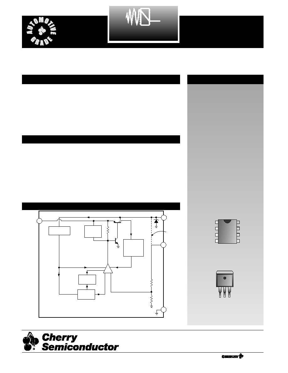
Features
Error
Amplifier
Thermal
Shutdown
Over
Voltage
Shutdown
V
IN
V
OUT
Bandgap
Reference
+ -
Current Limit
Sense
Current Source
(Circuit Bias)
Gnd
Sense*
* 8 Lead SO Narrow
D
2
PAK
s
Low Quiescent Current
(60µA @ 100µA load)
s
5V, ±2% Output
s
100mA Output Current
Capability
s
Fault Protection
+74V Peak Transient
Voltage
-15V Reverse Voltage
Short Circuit
Thermal Shutdown
Low Reverse Current
(Output to Input)
Package Options
CS8221
Micropower 5V, 100mA
Low Dropout Linear Regulator
CS8221
Description
The CS8221 is a precision 5V,
100mA micropower voltage regula-
tor with very low quiescent current
(60µA typical at 100µA load). The
5V output is accurate within ±2%
and supplies 100mA of load current
with a maximum dropout voltage
of only 600mV.
The regulator is protected against
reverse battery, short circuit, over
voltage, and over temperature con-
ditions. The device can withstand
74V load dump transients making it
suitable for use in automotive envi-
ronments.
Block Diagram
3L D
2
PAK
Tab (Gnd)
1
1. V
IN
2. Gnd
3. V
OUT
Absolute Maximum Ratings
Power Dissipation . . . . . . . . . . . . . . . . . . . . . . . . . . . . . . . . .Internally Limited
Transient Peak Voltage (60V Load Dump) . . . . . . . . . . . . . . . . . . . .-15V, 74V
Output Current . . . . . . . . . . . . . . . . . . . . . . . . . . . . . . . . . . . .Internally Limited
ESD Susceptibility (Human Body Model) . . . . . . . . . . . . . . . . . . . . . . . . . .2kV
Junction Temperature . . . . . . . . . . . . . . . . . . . . . . . . . . . . . . . . .-40°C to 150°C
Storage Temperature . . . . . . . . . . . . . . . . . . . . . . . . . . . . . . . . . .-55°C to 150°C
Lead Temperature Soldering
Reflow (SMD styles only) . . . . . .60 sec. max above 183°C, 230°C peak
1
V
IN
V
OUT
NC
Sense
Gnd
Gnd
Gnd
Gnd
8L SO Narrow
(Internally Fused Leads)
A Company
®
Rev. 12/28/98
Consult factory for TO-92.
Cherry Semiconductor Corporation
2000 South County Trail, East Greenwich, RI 02818
Tel: (401)885-3600 Fax: (401)885-5786
Email: info@cherry-semi.com
Web Site: www.cherry-semi.com

2
Electrical Characteristics:
6V ≤ V
IN
≤ 26V, I
OUT
= 1mA, -40° ≤ T
A
≤ 125°C, -40° ≤ T
J
≤ 150°C; unless otherwise specified.
PARAMETER
TEST CONDITIONS
MIN
TYP
MAX
UNIT
CS8221
Package Lead Description
PACKAGE LEAD #
LEAD SYMBOL
FUNCTION
s Output Stage
Output Voltage, V
OUT
9V<V
IN
<16V, 100µA ≤ I
OUT
≤ 100mA
4.90
5.00
5.10
V
6V ≤ V
IN
≤ 26V, 100µA ≤ I
OUT
≤ 100mA
4.85
5.00
5.15
V
Dropout Voltage (V
IN
-V
OUT
)
I
OUT
= 100mA
400
600
mV
I
OUT
= 100µA
100
150
mV
Load Regulation
V
IN
= 14V
5
50
mV
100µA ≤ I
OUT
≤ 100mA
Line Regulation
6V<V<26V
5
50
mV
I
OUT
= 1mA
Quiescent Current, (I
Q
)
I
OUT
= 100µA, V
IN
= 6V
60
120
µA
I
OUT
≤ 50mA
4
6
mA
I
OUT
≤ 100mA 12
20
mA
Ripple Rejection
7V ≤ V
IN
≤ 17V, I
OUT
= 100mA,
60
75
dB
f = 120Hz
Current Limit
125
200
mA
Short Circuit Output Current
V
OUT
= 0V
40
125
µA
Thermal Shutdown (Note 1)
150
180
°C
Overvoltage Shutdown
V
OUT
≤ 1V
30
34
38
V
Reverse Current
V
OUT
= 5V, V
IN
= 0V
100
500
µA
Note 1: This parameter is guaranteed by design, but not parametrically tested in production.
8L SO Narrow
3L
(Internally Fused Leads)
D
2
PAK
1
1
V
IN
Input voltage.
2
3
V
OUT
5V, ±2%, 100mA output.
3
–
NC
No connection.
4
–
Sense
Kelvin connection which allows remote sensing of the output
voltage for improved regulation. If remote sensing is not
required, connect to V
OUT
.
5,6,7,8
2
Gnd
Ground.

The output or compensation capacitor helps determine
three main characteristics of a linear regulator: start-up
delay, load transient response and loop stability.
The capacitor value and type should be based on cost,
availability, size and temperature constraints. A tantalum
or aluminum electrolytic capacitor is best, since a film or
ceramic capacitor with almost zero ESR can cause instabil-
ity. The aluminum electrolytic capacitor is the least expen-
sive solution, but, if the circuit operates at low tempera-
tures (-25°C to -40°C), both the value and ESR of the
capacitor will vary considerably. The capacitor manufac-
turers data sheet usually provides this information.
The value for the output capacitor C
OUT
shown in the test
and applications circuit should work for most applica-
tions, however it is not necessarily the optimized solution.
To determine an acceptable value for C
OUT
for a particular
application, start with a tantalum capacitor of the recom-
mended value and work towards a less expensive alterna-
tive part.
Step 1:
Place the completed circuit with a tantalum capac-
itor of the recommended value in an environmental cham-
ber at the lowest specified operating temperature and
monitor the outputs with an oscilloscope. A decade box
connected in series with the capacitor will simulate the
higher ESR of an aluminum capacitor. Leave the decade
box outside the chamber, the small resistance added by
the longer leads is negligible.
Step 2:
With the input voltage at its maximum value,
increase the load current slowly from zero to full load
while observing the output for any oscillations. If no oscil-
lations are observed, the capacitor is large enough to
ensure a stable design under steady state conditions.
Step 3:
Increase the ESR of the capacitor from zero using
the decade box and vary the load current until oscillations
appear. Record the values of load current and ESR that
cause the greatest oscillation. This represents the worst
case load conditions for the regulator at low temperature.
Step 4
: Maintain the worst case load conditions set in step
3 and vary the input voltage until the oscillations increase.
This point represents the worst case input voltage condi-
tions.
Step 5:
If the capacitor is adequate, repeat steps 3 and 4
with the next smaller valued capacitor. A smaller capaci-
C
1
**
0.1
mF
V
IN
Sense*
V
OUT
CS8221
C
2
***
10
mF
Gnd
Output Stage Protection
The output stage is protected against overvoltage, short
circuit and thermal runaway conditions (Figure 1).
If the input voltage rises above 34V (typ), the output shuts
down. This response protects the internal circuitry and
enables the IC to survive unexpected voltage transients.
Should the junction temperature of the power device
exceed 180˚C (typ) the power transistor is turned off.
Thermal shutdown is an effective means to prevent die
overheating since the power transistor is the principle heat
source in the IC.
I
OUT
V
OUT
V
IN
Load
Dump
Short
Circuit
Thermal
Shutdown
> 30V
3
CS8221
Application Notes
Application & Test Diagram
Voltage Reference and Output Circuitry
Stability Considerations
Circuit Description
Figure 1. Typical Circuit Waveforms for Output Stage Protection.
* 8 Lead SO Narrow only
**C1 is required if regulator is distant from power source filter.
***C2 is required for stability.
4
tor will usually cost less and occupy less board space. If
the output oscillates within the range of expected operat-
ing conditions, repeat steps 3 and 4 with the next larger
standard capacitor value.
Step 6:
Test the load transient response by switching in
various loads at several frequencies to simulate its real
working environment. Vary the ESR to reduce ringing.
Step 7:
Remove the unit from the environmental chamber
and heat the IC with a heat gun. Vary the load current as
instructed in step 5 to test for any oscillations.
Once the minimum capacitor value with the maximum
ESR is found, a safety factor should be added to allow for
the tolerance of the capacitor and any variations in regula-
tor performance. Most good quality aluminum electrolytic
capacitors have a tolerance of ±20% so the minimum value
found should be increased by at least 50% to allow for this
tolerance plus the variation which will occur at low tem-
peratures. The ESR of the capacitor should be less than
50% of the maximum allowable ESR found in step 3
above.
The maximum power dissipation for a single output regu-
lator (Figure 2) is:
P
D(max)
= {V
IN(max)
–V
OUT(min)
}I
OUT(max)
+V
IN(max)
I
Q
(1)
where:
V
IN(max)
is the maximum input voltage,
V
OUT(min)
is the minimum output voltage,
I
OUT(max)
is the maximum output current for the applica-
tion, and
I
Q
is the quiescent current the regulator consumes at
I
OUT(max)
.
Once the value of P
D(max)
is known, the maximum permis-
sible value of R
QJA
can be calculated:
R
QJA
=
(2)
Figure 2. Single output regulator with key performance parameters
labeled.
The value of R
QJA
can then be compared with those in
the package section of the data sheet. Those packages
with R
QJA
's less than the calculated value in equation 2
will keep the die temperature below 150°C.
In some cases, none of the packages will be sufficient to
dissipate the heat generated by the IC, and an external
heatsink will be required.
A heat sink effectively increases the surface area of the
package to improve the flow of heat away from the IC and
into the surrounding air.
Each material in the heat flow path between the IC and the
outside environment will have a thermal resistance. Like
series electrical resistances, these resistances are summed
to determine the value of R
QJA
:
R
QJA
= R
QJC
+ R
QCS
+ R
QSA
(3)
where:
R
QJC
= the junction–to–case thermal resistance,
R
QCS
= the case–to–heatsink thermal resistance, and
R
QSA
= the heatsink–to–ambient thermal resistance.
R
QJC
appears in the package section of the data sheet. Like
R
QJA
, it too is a function of package type. R
QCS
and R
QSA
are functions of the package type, heatsink and the inter-
face between them. These values appear in heat sink data
sheets of heat sink manufacturers.
Heat Sinks
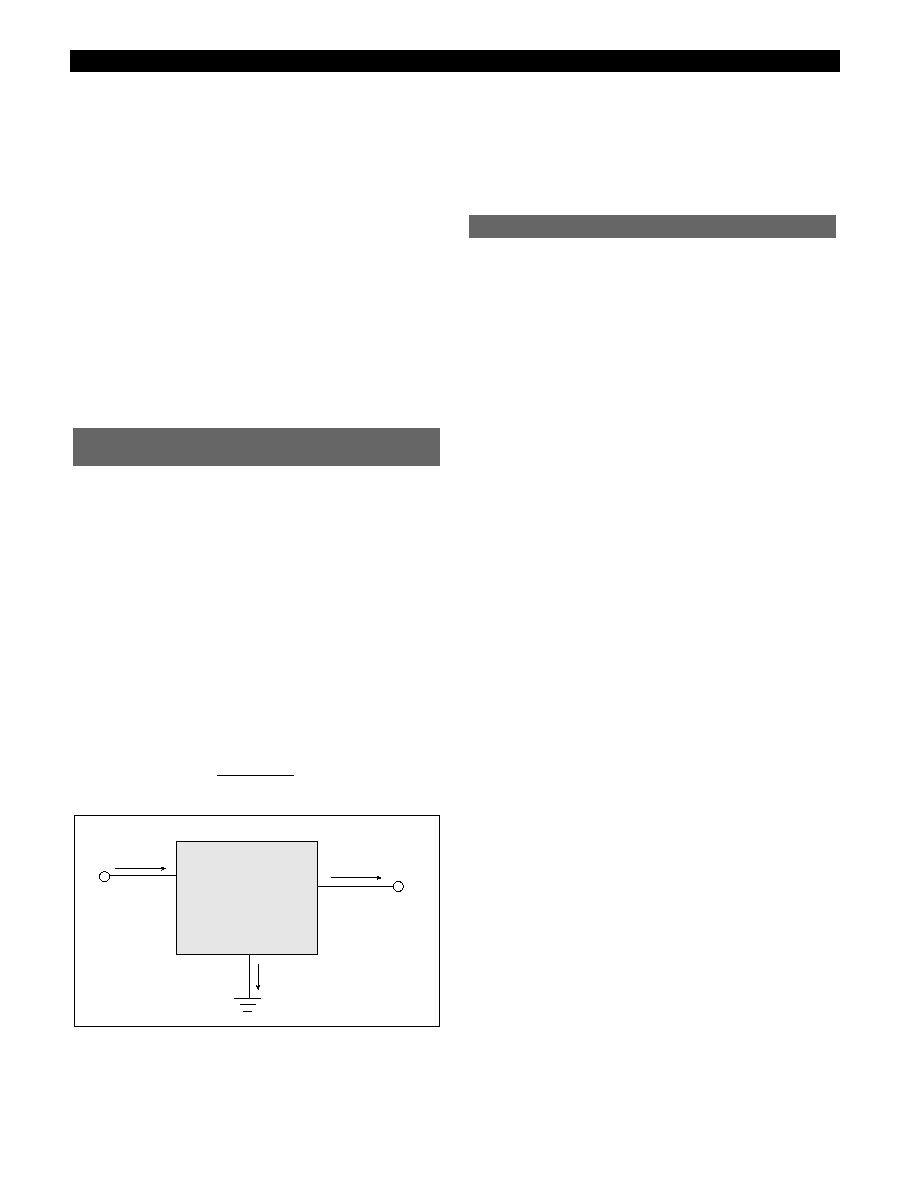
V
IN
CS8221
V
OUT
I
OUT
I
IN
I
Q
150°C - T
A
P
D
Calculating Power Dissipation
in a Single Output Linear Regulator
Application Notes: continued
CS8221
5
Thermal Data
8 Lead
3 Lead
SO Narrow
D
2
PAK
(internally fused leads)
R
QJC
typ
25
4.2
˚C/W
R
QJA
typ
110
10-50*
˚C/W
*Depending on thermal properties of substrate. R
QJA
= R
QJC
+ R
QCA
D
Lead Count
Metric
English
Max
Min
Max
Min
8L SO Narrow
5.00
4.80
.197
.189
(internally fused leads)
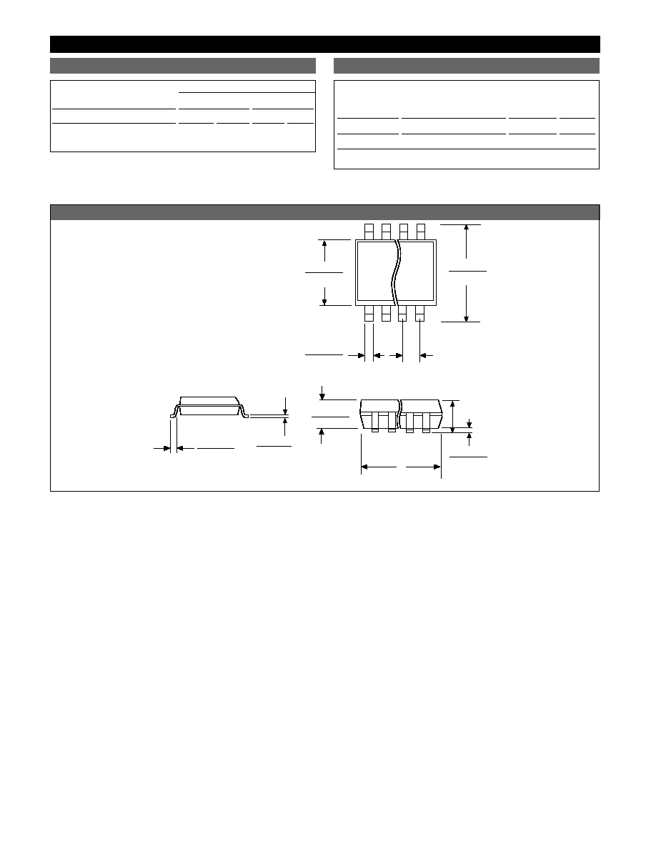
Package Specification
PACKAGE DIMENSIONS IN mm (INCHES)
PACKAGE THERMAL DATA
CS8221
Surface Mount Narrow Body (D); 150 mil wide
1.27 (.050) BSC
0.51 (.020)
0.33 (.013)
6.20 (.244)
5.80 (.228)
4.00 (.157)
3.80 (.150)
1.57 (.062)
1.37 (.054)
D
0.25 (0.10)
0.10 (.004)
1.75 (.069) MAX
1.27 (.050)
0.40 (.016)
REF: JEDEC MS-012
0.25 (.010)
0.19 (.008)