1
Features
Overvoltage
Shutdown
Thermal
Shutdown
Control
Circuit
Current
Limit
V
CC
V
IN
Gnd
OUT
s
Low Output Saturation
Voltage
0.22V at I
OUT
= 125mA
0.33V at I
OUT
= 225mA
s
Overmolded Package
s
On-Chip Flyback Diode
s
Fault Protection
Over voltage
Shutdown (32V, typ)
Thermal Shutdown
(165°C, typ)
Short Circuit Limiting
(1.1A typ)
-50V Reverse Transient
Protection
60V Load Dump
Protection
Reverse Battery
s
Low Quiescent Current
(Off State)
s
ESD Protected
Package Options
5 Lead TO-220
Overmolded
CS8240
500mA High Side (PNP) Driver
with On-Chip Flyback Diode
Description
Block Diagram
Absolute Maximum Ratings
The CS8240 is a fast, PNP high side
driver capable of delivering up to
500mA into a resistive or inductive
load in harsh automotive or industrial
environments. An internal flyback
diode clamp is incorporated for induc-
tive loads. The input (V
IN
) is TTL and
CMOS compatible and has hysteresis to
minimize the effects of noise. When the
input is high, the output is on. When
the input is low, the output is off and
the supply voltage quiescent current is
very low (<1.0µA, typ). For device pro-
tection, the CS8240 incorporates ther-
mal shutdown, short circuit current
limiting, over voltage shutdown, and
reverse battery protection. The CS8240
can withstand supply voltage tran-
sients of 60V (min) and -50V.
The CS8240 is available in an overmold-
ed 5 lead TO-220 package and is a com-
petitive replacement for the LM-1921,
LM-1951, LM-1952, MC-3399, and L-9350.
CS8240
Supply Voltage.....................................................................................6V to +26V
Overvoltage Protection ....................................................................................60V
Reverse Voltage ........................................................................................-16V DC
.........................................................................................-50V Transient
Internal Power Dissipation .....................................................Internally limited
Logic Input Voltage ..........................................................................-0.3V to 7.0V
Junction Temperature Range.....................................................-40°C to +150°C
Storage Temperature Range ......................................................-55°C to +165°C
Lead Temperature Soldering
Wave Solder(through hole styles only).............10 sec. max, 260°C peak
Electrostatic Discharge (Human Body Model) ............................................2kV
1 V
CC
2 OUT
3 NC
4 Gnd
5 V
IN
1
A Company
®
Rev. 1/27/98
Cherry Semiconductor Corporation
2000 South County Trail, East Greenwich, RI 02818
Tel: (401)885-3600 Fax: (401)885-5786
Email: info@cherry-semi.com
Web Site: www.cherry-semi.com
2
Electrical Characteristics:
-40°C ≤ T
A
≤ 125°C, -40°C ≤ T
J
≤ 150°C, unless otherwise noted.
PARAMETER
TEST CONDITIONS
MIN
TYP
MAX
UNIT
CS8240
Package Lead Description
PACKAGE LEAD #
LEAD SYMBOL
FUNCTION
5 Lead TO-220
1
V
CC
Supply voltage to IC. Supplies load current through
output PNP.
2
OUT
Collector of output PNP, current to load is sourced
from this lead.
3
NC
No connection.
4
Gnd
Ground.
5
V
IN
Input voltage to control output. Logic high turns out-
put on. Logic low turns output off.
s General Characteristics
Operating Supply Voltage
6.0
V
Quiescent Current
V
CC
= 12V, V
IN
≤ V
IN(LOW)
1
100
µA
V
IN
≥ V
IN(HI)
, R
LOAD
= 50Ω,
6 ≤ V
CC
≤ 20V
16
30
mA
20V ≤ V
CC
≤ 24V
25
50
mA
s Output Stage
Output Saturation Voltage
V
IN
≤ V
IN(HI)
, V
CC
= 6.0V,
I
LOAD
= 125mA
0.22
0.5
V
V
CC
= 14V, I
LOAD
= 225mA
0.33
0.7
V
Output Leakage Current
Input ≤ V
IN(L)
, V
CC
= 12V, V
OUT
= 0V
1
150
µA
Negative Output Clamp
I
CLAMP
= 100mA, V
CC
= 12V
-18
-15.5
-12
V
Turn On Delay Time
V
CC
= 12V, I
LOAD
= 150mA
5
20
us
Turn Off Delay Time
V
CC
= 12V, I
LOAD
= 150mA
5
20
us
s Input Stage
Input Voltage
Logic = High, V
CC
= 12V Turn ON
0.8
1.45
V
Logic = Low, V
CC
= 12V Turn OFF
1.2
2.0
V
Input Current
V
IN
= 5.5V
100
200
µA
V
IN
= 0.8V
15
50
µA
s Protection Circuitry
Overvoltage Shutdown
V
IN
≥ V
IN(HI)
26
32
V
Output Short Circuit Current V
IN
≥ V
IN(HI)
, V
CC
= 12V, V
OUT
= 0V
0.55
1.1
2.5
A
Thermal Shutdown
150
165
°C
4
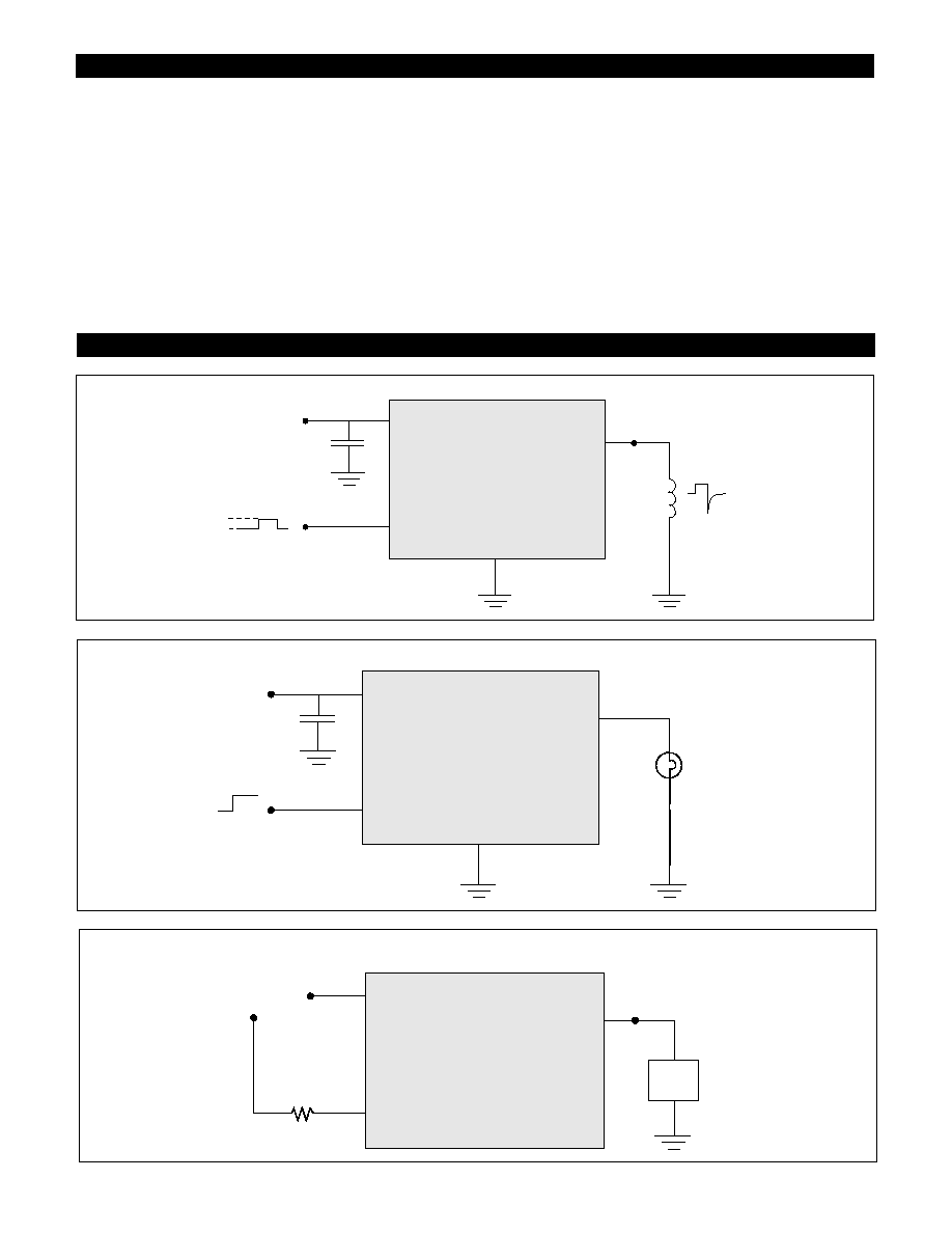
Circuit Description
Typical Application Circuits
CS8240
0.1
mF
1
2
3
5
CS8240
V
CC
GE194
0.1
mF
1
2
3
5
CS8240
0V
5V
V
CC
*
Solenoid Driver
V
CC
= 6.0V to 26.0V
V
BAT
CS8240
LOAD
V
IGNITION
15k
W
Lamp Driver
Controlled High Side Switch
Input Stage
The input stage is a self biased band gap based circuit with a
positive going trip point of 1.45V (typ) and a negative going
trip point of 1.20V (typ) (250mV of hysteresis). When the input
voltage is below the positive trip point, the quiescent current
of the supply voltage line is less than 1µA, (typ). When the
input voltage exceeds the positive trip point (1.45V, typ), the
input stage “wakes up” the rest of the CS8240 circuitry and
turns on the output stage.
Output Stage
The output stage is built around a high current PNP output
transistor. A control amplifier monitors the saturation voltage
of the output PNP and maintains a balance of low saturation
voltage and minimum base drive to the PNP for the given out-
put current. The base drive of the PNP is the dominant com-
ponent of the quiescent current of the CS8240 and is depen-
dent on the level of output current.
Short circuit protection (1.1A, typ) is also incorporated in the
output stage.
Protection Circuitry
In addition to the short circuit protection mentioned above,
the CS8240 also incorporates a thermal shutdown circuit
(165°C, typ) and a high voltage shutdown circuit (33V, typ),
both of which cut off the drive to the PNP output transistor
when excessive current is drawn. Inherent in the design of the
CS8240 is transient protection to +60V and -50V on the supply
line. The CS8240 is ESD protected in excess of 2kV (Human
Body Model).
Part Number
Description
CS8240YTFVA5
5 Lead Overmolded TO-220
Vertical
5
CS8240
Thermal Data
5 Lead TO-220 (Overmolded)
R
Q
JC
typ
4.0
˚C/W
R
Q
JA
typ
50
˚C/W
Package Specification
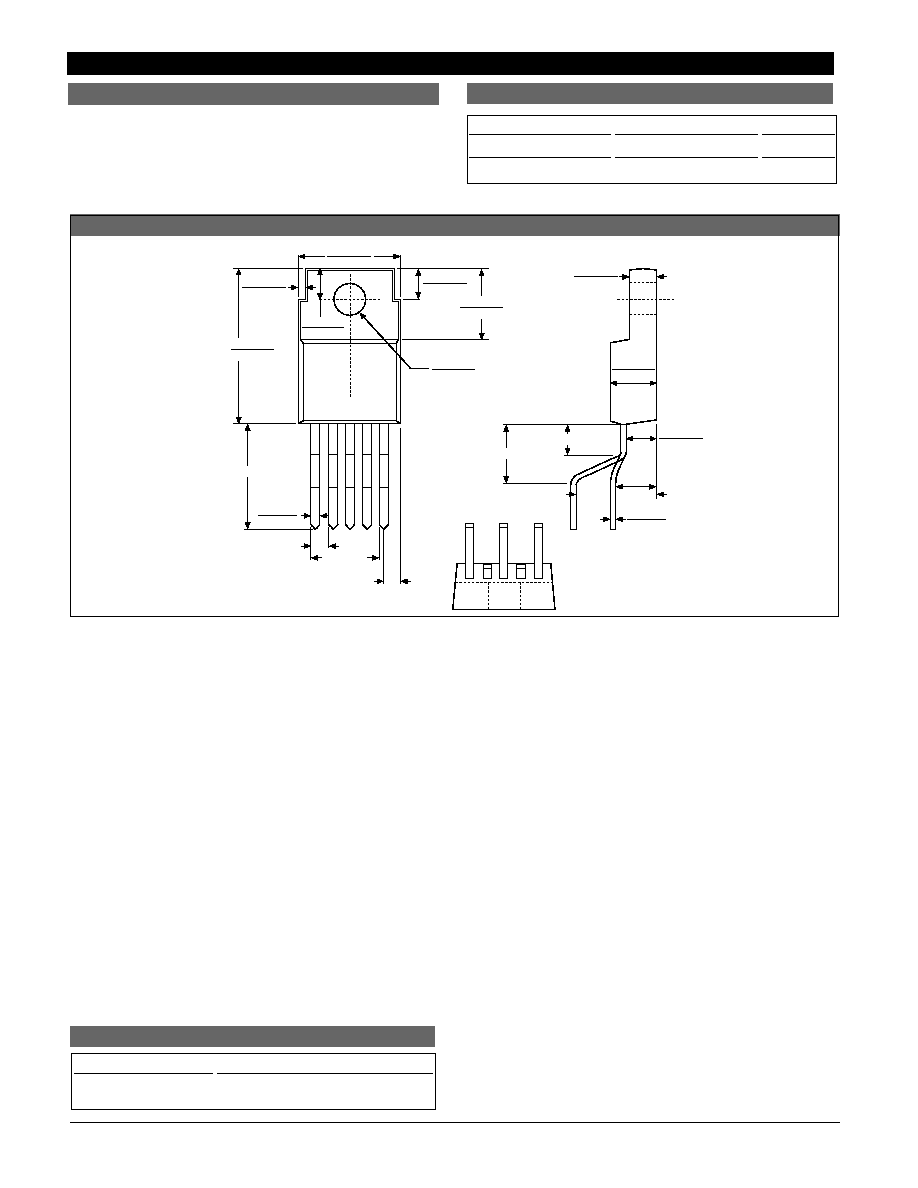
PACKAGE DIMENSIONS IN mm (INCHES)
Ordering Information
PACKAGE THERMAL DATA
Rev. 1/27/98
© 1999 Cherry Semiconductor Corporation
Cherry Semiconductor Corporation reserves the
right to make changes to the specifications without
notice. Please contact Cherry Semiconductor
Corporation for the latest available information.
5 Lead Overmolded TO-220 (TFVA) Vertical
10.3 (.405)
10.0 (.395)
.761 (.030)
.508 (.020)
15.6 (.614)
15.3 (.604)
3.17 (.125)
2.92 (.115)
7.18 (.283)
6.94 (.273)
3.30 (.130)
2.89 (.114)
10.4 (.409)
.94 (.037)
.69 (.027)
1.70 (.067)
6.80 (.268)
1.68 (.066) TYP
3.30 (.130)
3.05 (.120)
DIA
2.79 (.110)
2.54 (.100)
4.70 (.185)
4.44 (.175)
5.89 (.232)
3.10 (.122)
.56 (.022)
.36 (.014)
4.01
(.158)
8.05 (.317)
Note:
Leads maintain
a right angle
with respect to
the package
body to within
± .015≤.
3.18 (.125)
2.92 (.115)