www.chinfa.com
MODEL NO.
INPUT
VOLTAGE
OUTPUT
WATTAGE
OUTPUT
VOLTAGE
OUTPUT
CURRENT
EFF.
(min.)
75%
FDD05 - 05S0
4.5~5.5 VDC
5 WATTS
+ 5 VDC
1000 mA
80%
FDD05 - 12S0
4.5~5.5 VDC
6 WATTS
+ 12 VDC
500 mA
81%
FDD05 - 15S0
4.5~5.5 VDC
6 WATTS
+ 15 VDC
400 mA
75%
FDD05 - 05D0
4.5~5.5 VDC
5 WATTS
5 VDC
500 mA
80%
FDD05 - 12D0
4.5~5.5 VDC
6 WATTS
12 VDC
81%
FDD05 - 15D0
4.5~5.5 VDC
6 WATTS
15 VDC
250 mA
200 mA
Single Output Models
Dual Output Models
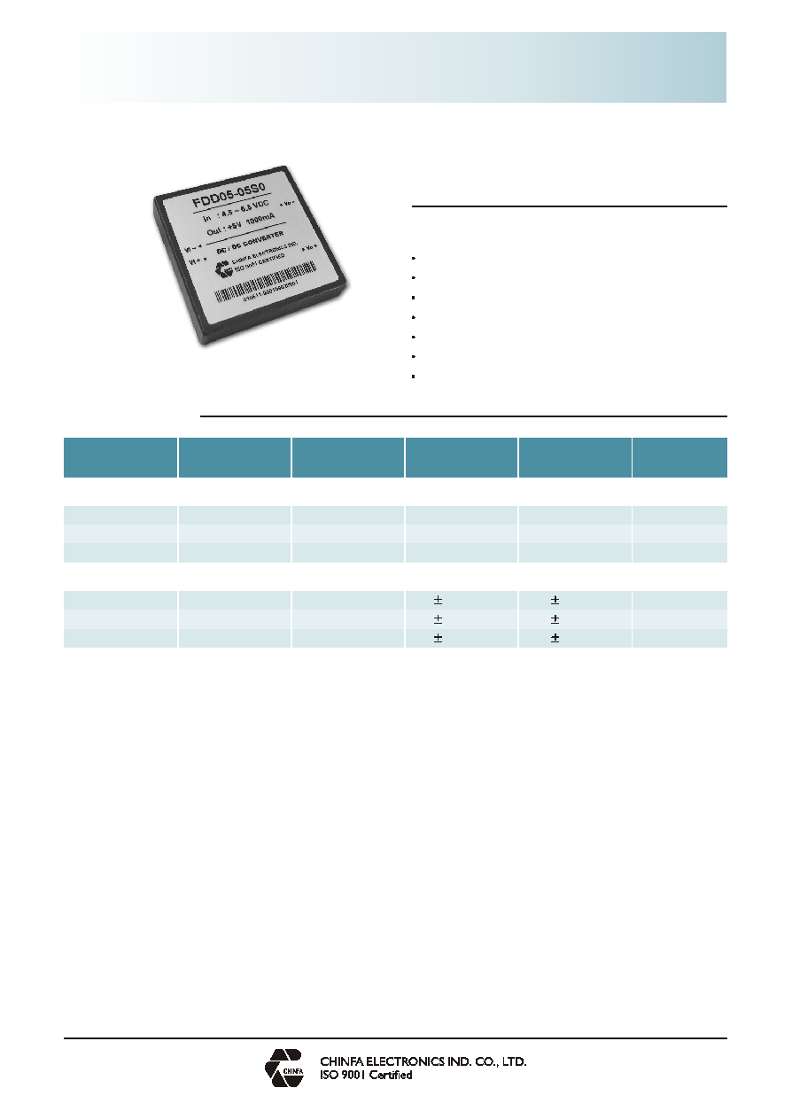
DC - DC CONVERTER
5 ~ 6W 5V INPUT MODEL
FEATURES
INPUT 4.5 V ~ 5.5 V
INPUT FILTER BUILT - IN
I/O
ISOLATION
HIGH EFFICIENCY UP TO 81 %
SHORT CIRCUIT PROTECTION
2 " x 2 " METAL CASE
2 YEARS WARRANTY
MODEL LIST
FDD05 SERIES
sales@chinfa.com
sales@chinfa.com
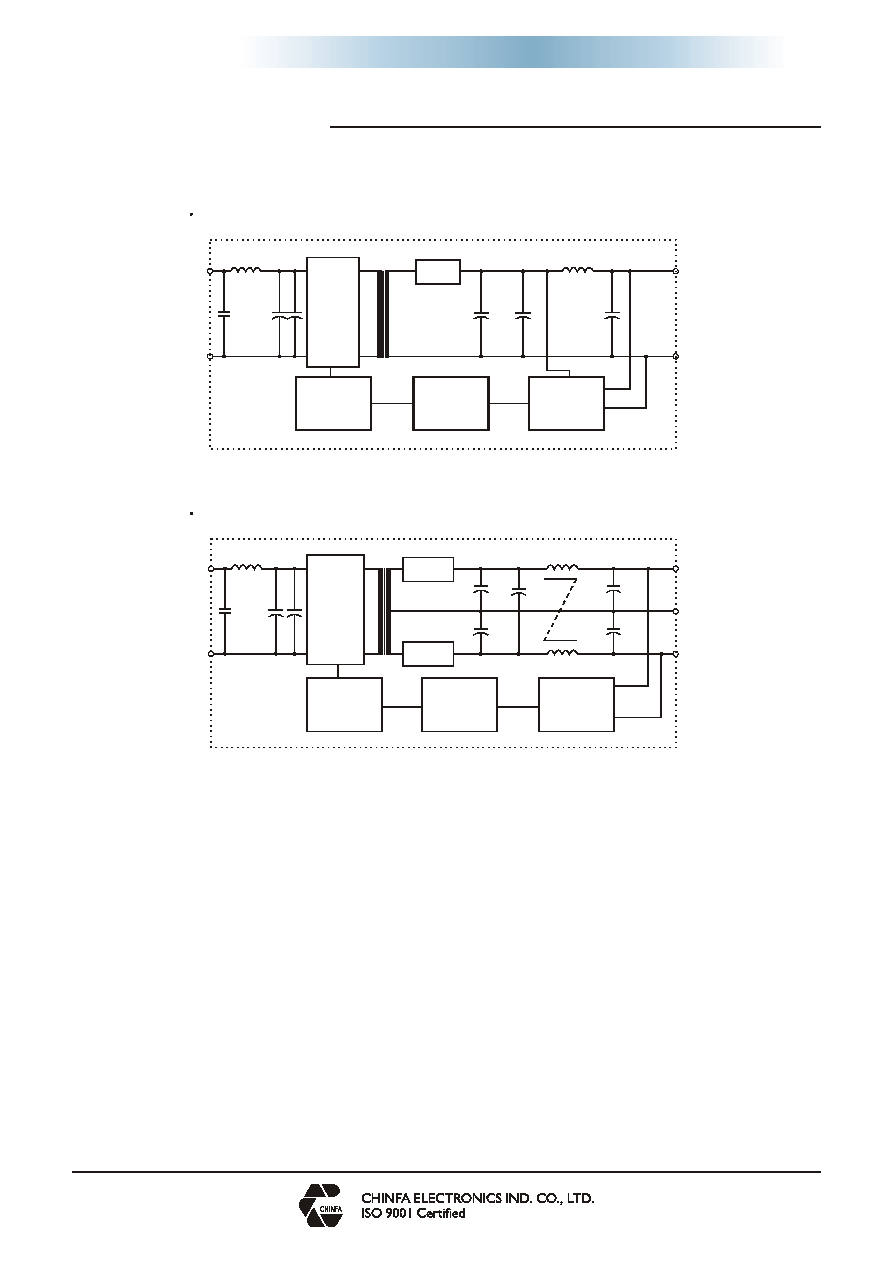
CIRCUIT SCHEMATIC
Vo -
Vo +
Switching
Device
Rectifier
Vi +
Vi -
com
Vi +
Vi -
Vo -
Vo +
Rectifier
Switching
Device
FDD05 SERIES
5V INPUT MODEL
Block diagram for FDD05 5V input model with dual output
Block diagram for FDD05 5V input model with single output
Reference &
Error Amp.
Opto -
Isolation
PWM
Controller
Rectifier
PWM
Controller
Opto -
Isolation
Reference &
Error Amp.
www.chinfa.com
www.chinfa.com
FDD05 SERIES
5V INPUT MODEL
Characteristics
Conditions
min.
typ.
max.
unit
Switching frequency
Isolation voltage
Isolation resistance
Ambient temperature
Case temperature
Vi nom, Io nom
Input / Output
Input / Output, @ 500VDC
Operating at Vi nom, Io nom
Operating at Vi nom, Io nom
K H z
1,500
VDC
M
100
-25
+ 71
o
C
o
C
Storage temperature
M.T.B.F.
Non operational
According to MIL-HDBK-217F, GF40
-40
o
C
661,000
Characteristics
Conditions
min.
typ.
max.
unit
Input voltage range
No load input current
Input voltage w/o damage
Ta min ...Ta max, Io nom
Vi nom, Io = 0
Io nom
4.5
5
5.5
VDC
mA
7
VDC
Characteristics
Conditions
min.
unit
Output voltage accuracy
Minimum load
Line regulation
Load regulation
Transient recovery time
Vi nom, Io nom
Vi nom
single output models
dual output models (each output)
Io nom, Vi min ...Vi max
Vi nom, Io 0 ...Io nom, for single output models
Vi nom, Io min ...Io nom, for dual output models
Vi nom, Io nom ... 1/2 Io nom
typ.
max.
0
20
%
%
%
%
2
1
2
5
%
0.02
o
% / C
mV
Input reversed
Shunt diode built in, external fuse recommended
Output short circuit
Continuous
CONTROL AND PROTECTION
Startup voltage
Io nom
15
4
VDC
Input filter
Pi type
INPUT SPECIFICATIONS
OUTPUT SPECIFICATIONS
Efficiency
Up to 81%, See model list
Temperature coefficient
Ripple & noise
Vi nom, Io nom, BW = 20MHz
Vi nom, Io nom, Po / Pi
Vi nom, Io nom
500
100
S
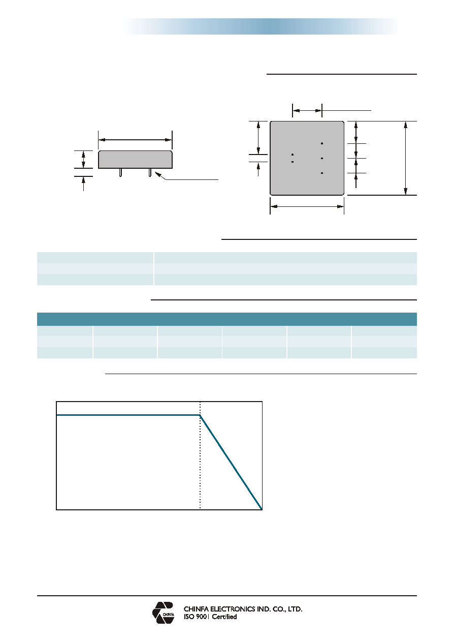
Derating
Vi nom
o
% / C
See derating curve
+100
o
All Specifications Typical At Nominal Line, Full Load, 25 C Unless Otherwise Noticed
SPECIFICATION
200
Dimension
L50.8 x W50.8 x H11.9
Cooling
Free air convection
Hrs
mm
Case material
Metal
GENERAL
+100
%
sales@chinfa.com
sales@chinfa.com
MECHANISM & PIN CONFIGURATION
PHYSICAL CHARACTERISTICS
CASE SIZE
CASE MATERIAL
WEIGHT
50.8 x 50.8 x 11.9 mm 2 x 2 x 0.47 inches
Metal
65 g (typ.)
PIN ASSIGNMENT
PIN NO.
SINGLE
DUAL
Vi+
Vo+
Vi -
Vi+
Vo -
Vi -
DERATING
NATURAL
CONVECTION
COOLING
0
100
o
Ambient Temperature [ C ]
71
100
-25
P
o
w
e
r
o
u
t
[
%
]
1
GENERAL
NO PIN
com
Vo+
mm [inch]
50.80 [2.00]
11.94 [0.47]
DIA 1.00 [0.04]
5.08 [0.20]
2
3
4
5
Vo -
20.32 [0.80]
BOTTOM VIEW
3
4
5
1
2
15.24 [0.60]
10.16 [0.40]
10.16 [0.40]
5
0
.
8
0
[
2
.
0
0
]
50.80 [2.00]
22.86 [0.90]
5.08 [0.20]
BOTTOM VIEW
FDD05 SERIES
5V INPUT MODEL
www.chinfa.com