 | –≠–ª–µ–∫—Ç—Ä–æ–Ω–Ω—ã–π –∫–æ–º–ø–æ–Ω–µ–Ω—Ç: Pm39LV512 | –°–∫–∞—á–∞—Ç—å:  PDF PDF  ZIP ZIP |

FEATURES
∑
Single Power Supply Operation
- Low voltage range: 2.7 V - 3.6 V
∑ Memory Organization
- Pm39LV512: 64K x 8 (512 Kbit)
- Pm39LV010: 128K x 8 (1 Mbit)
- Pm39LV020: 256K x 8 (2 Mbit)
- Pm39LV040: 512K x 8 (4 Mbit)
∑ High Performance Read
- 55/70 ns access time
∑ Cost Effective Sector/Block Architecture
- Uniform 4 Kbyte sectors
- Uniform 64 Kbyte blocks (sector group - except
Pm39LV512)
∑ Data# Polling and Toggle Bit Features
∑ Hardware Data Protection
∑ Automatic Erase and Byte Program
- Build-in automatic program verification
- Typical 16 µs/byte programming time
- Typical 55 ms sector/block/chip erase time
∑ Low Power Consumption
- Typical 4 mA active read current
- Typical 8 mA program/erase current
- Typical 0.1 µA CMOS standby current
∑ High Product Endurance
- Guarantee 100,000 program/erase cycles per
single sector (preliminary)
- Minimum 20 years data retention
∑ Industrial Standard Pin-out and Packaging
- 32-pin (8 mm x 14 mm) VSOP
- 32-pin PLCC
- Optional lead-free (Pb-free) package
GENERAL DESCRIPTION
The Pm39LV512/010/020/040 are 512 Kbit/1 Mbit/2 Mbit/4 Mbit 3.0 Volt-only Flash Memories. These devices are
designed to use a single low voltage, range from 2.7 Volt to 3.6 Volt, power supply to perform read, erase and
program operations. The 12.0 Volt V
PP
power supply for program and erase operations are not required. The devices
can be programmed in standard EPROM programmers as well.
The memory array of Pm39LV512 is divided into uniform 4 Kbyte sectors for data or code storage. The memory
arrays of Pm39LV010/020/040 are divided into uniform 4 Kbyte sectors or uniform 64 Kbyte blocks (sector group -
consists of sixteen adjacent sectors). The sector or block erase feature allows users to flexibly erase a memory
area as small as 4 Kbyte or as large as 64 Kbyte by one single erase operation without affecting the data in others.
The chip erase feature allows the whole memory array to be erased in one single erase operation. The devices can
be programmed on a byte-by-byte basis after performing the erase operation.
The devices have a standard microprocessor interface as well as a JEDEC standard pin-out/command set. The
program operation is executed by issuing the program command code into command register. The internal control
logic automatically handles the programming voltage ramp-up and timing. The erase operation is executed by
issuing the chip erase, block, or sector erase command code into command register. The internal control logic
automatically handles the erase voltage ramp-up and timing. The preprogramming on the array which has not been
programmed is not required before an erase operation. The devices offer Data# Polling and Toggle Bit functions, the
progress or completion of program and erase operations can be detected by reading the Data# Polling on I/O7 or
the Toggle Bit on I/O6.
The Pm39LV512/010/020/040 are manufactured on PMC's advanced nonvolatile CMOS technology, P-FLASHTM.
The devices are offered in 32-pin VSOP and PLCC packages with access time of 55 and 70 ns.
PMC
512 Kbit / 1Mbit / 2Mbit / 4Mbit 3.0 Volt-only CMOS Flash Memory
Programmable Microelectronics Corp.
Issue Date: December, 2003 Rev:1.2
Pm39LV512 / Pm39LV010 / Pm39LV020 / Pm39LV040
1
Programmable Microelectronics Corp.
Issue Date: December, 2003 Rev: 1.2
PMC
Pm39LV512 / Pm39LV010 / Pm39LV020 / Pm39LV040
2
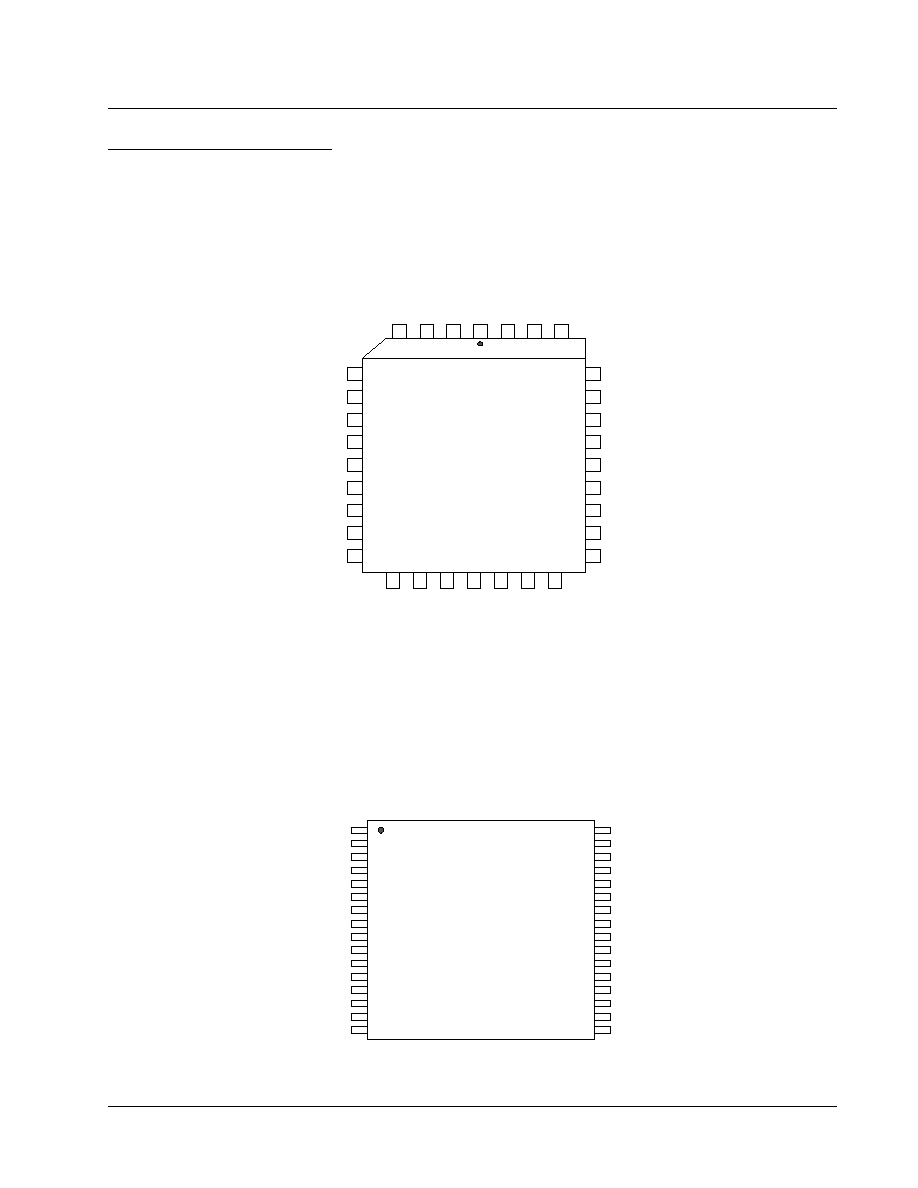
CONNECTION DIAGRAMS
32-Pin PLCC
20
19
18
17
16
15
14
5
6
7
8
9
10
11
12
13
1
2
3
4
32
31
30
A12
A15
NC
V
CC
WE#
NC
I/O1
GND
I/O2
I/O3
I/O4
I/O5
I/O6
I/O0
A 0
A 1
A 2
A 3
A 4
A 5
A 6
A 7
29
28
27
26
25
24
23
22
21
A14
A13
A 8
A 9
A11
O E #
A10
C E #
I/O7
A14
A13
A 8
A 9
A11
O E #
A10
C E #
I/O7
A14
A13
A 8
A 9
A11
O E #
A10
C E #
I/O7
A14
A13
A 8
A 9
A11
O E #
A10
C E #
I/O7
I/O1
GND
I/O2
I/O3
I/O4
I/O5
I/O6
I/O1
GND
I/O2
I/O3
I/O4
I/O5
I/O6
I/O1
GND
I/O2
I/O3
I/O4
I/O5
I/O6
I/O0
A 0
A 1
A 2
A 3
A 4
A 5
A 6
A 7
I/O0
A 0
A 1
A 2
A 3
A 4
A 5
A 6
A 7
I/O0
A 0
A 1
A 2
A 3
A 4
A 5
A 6
A 7
A12
A15
V
CC
WE#
NC
NC
NC
A12
A15
V
CC
WE#
A12
A15
V
CC
WE#
A16
A16
A16
A18
A17
A17
NC
39LV512
39LV010
39LV020
39LV040
39LV040
39LV020
39LV010
39LV512
3 9 L V 5 1 2
3 9 L V 0 1 0 3 9 L V 0 2 0
3 9 L V 0 4 0
3 9 L V 0 4 0
3 9 L V 0 2 0 3 9 L V 0 1 0
3 9 L V 5 1 2
1
2
3
4
5
6
7
8
9
10
11
12
13
14
15
16
32
31
30
29
28
27
26
25
24
23
22
21
20
19
18
17
32-Pin VSOP
I/O4
O E #
A 1 0
C E #
I/O7
I/O6
I/O5
I/O3
G N D
I/O2
I/O1
I/O0
A 0
A 1
A 2
A 3
39LV512
39LV512
A 1 1
A 9
A 8
A 1 3
A 1 4
W E #
V
C C
N C
A 1 5
A 1 2
A 7
A 6
A 5
A 4
N C
N C
39LV040
A 1 1
A 9
A 8
A 1 3
A 1 4
W E #
V
C C
A 1 5
A 1 2
A 7
A 6
A 5
A 4
A 1 6
A 1 8
A 1 7
39LV020
A 1 1
A 9
A 8
A 1 3
A 1 4
W E #
V
C C
N C
A 1 5
A 1 2
A 7
A 6
A 5
A 4
A 1 6
A 1 7
39LV010
A 1 1
A 9
A 8
A 1 3
A 1 4
W E #
V
C C
N C
A 1 5
A 1 2
A 7
A 6
A 5
A 4
A 1 6
N C
I/O4
O E #
A 1 0
C E #
I/O7
I/O6
I/O5
I/O3
G N D
I/O2
I/O1
I/O0
A 0
A 1
A 2
A 3
39LV040
I/O4
O E #
A 1 0
C E #
I/O7
I/O6
I/O5
I/O3
G N D
I/O2
I/O1
I/O0
A 0
A 1
A 2
A 3
39LV020
I/O4
O E #
A 1 0
C E #
I/O7
I/O6
I/O5
I/O3
G N D
I/O2
I/O1
I/O0
A 0
A 1
A 2
A 3
39LV010
Programmable Microelectronics Corp.
Issue Date: December, 2003 Rev: 1.2
PMC
Pm39LV512 / Pm39LV010 / Pm39LV020 / Pm39LV040
3
PRODUCT ORDERING INFORMATION
Pm39LV0x0 -70 J C E
Temperature Range
C = Commercial (0∞C to +70∞C)
Package Type
J = 32-pin Plastic J-Leaded Chip Carrier (32J)
V = 32-pin Thin Small Outline Package
(VSOP - 8 mm x 14 mm)(32V)
Speed Option
PMC Device Number
Pm39LV512 (512 Kbit)
Pm39LV010 (1 Mbit)
Pm39LV020 (2 Mbit)
Pm39LV040 (4 Mbit)
r
e
b
m
u
N
t
r
a
P
t
C
C
A
)
s
n
(
e
g
a
k
c
a
P
e
g
n
a
R
e
r
u
t
a
r
e
p
m
e
T
E
C
J
0
7
-
2
1
5
V
L
9
3
m
P
0
7
J
2
3
l
a
i
c
r
e
m
m
o
C
)
C
∞
0
7
+
o
t
C
∞
0
(
C
J
0
7
-
2
1
5
V
L
9
3
m
P
E
C
V
0
7
-
2
1
5
V
L
9
3
m
P
V
2
3
C
V
0
7
-
2
1
5
V
L
9
3
m
P
E
C
J
0
7
-
0
1
0
V
L
9
3
m
P
0
7
J
2
3
C
J
0
7
-
0
1
0
V
L
9
3
m
P
E
C
V
0
7
-
0
1
0
V
L
9
3
m
P
V
2
3
C
V
0
7
-
0
1
0
V
L
9
3
m
P
E
C
J
0
7
-
0
2
0
V
L
9
3
m
P
0
7
J
2
3
C
J
0
7
-
0
2
0
V
L
9
3
m
P
E
C
V
0
7
-
0
2
0
V
L
9
3
m
P
V
2
3
C
V
0
7
-
0
2
0
V
L
9
3
m
P
E
C
J
0
7
-
0
4
0
V
L
9
3
m
P
0
7
J
2
3
C
J
0
7
-
0
4
0
V
L
9
3
m
P
E
C
V
0
7
-
0
4
0
V
L
9
3
m
P
V
2
3
C
V
0
7
-
0
4
0
V
L
9
3
m
P
Environmental Attribute
E = Lead-free (Pb-free) Package
Blank = Standard Package
Programmable Microelectronics Corp.
Issue Date: December, 2003 Rev: 1.2
PMC
Pm39LV512 / Pm39LV010 / Pm39LV020 / Pm39LV040
4
PIN DESCRIPTIONS
L
O
B
M
Y
S
E
P
Y
T
N
O
I
T
P
I
R
C
S
E
D
A
-
0
A
S
M
)
1
(
T
U
P
N
I
y
ll
a
n
r
e
t
n
i
e
r
a
s
e
s
s
e
r
d
d
A
.
t
u
p
n
i
s
e
s
s
e
r
d
d
a
y
r
o
m
e
m
r
o
F
:
s
t
u
p
n
I
s
s
e
r
d
d
A
.
e
l
c
y
c
e
t
i
r
w
a
g
n
i
r
u
d
#
E
W
f
o
e
g
d
e
g
n
il
l
a
f
e
h
t
n
o
d
e
h
c
t
a
l
#
E
C
T
U
P
N
I
r
o
f
s
e
i
r
t
i
u
c
r
i
c
l
a
n
r
e
t
n
i
s
'
e
c
i
v
e
d
e
h
t
s
e
t
a
v
i
t
c
a
w
o
l
s
e
o
g
#
E
C
:
e
l
b
a
n
E
p
i
h
C
o
t
n
i
s
e
h
c
t
i
w
s
d
n
a
e
c
i
v
e
d
e
h
t
s
t
c
e
l
e
s
e
d
h
g
i
h
s
e
o
g
#
E
C
.
n
o
i
t
a
r
e
p
o
e
c
i
v
e
d
.
n
o
i
t
p
m
u
s
n
o
c
r
e
w
o
p
e
h
t
e
c
u
d
e
r
o
t
e
d
o
m
y
b
d
n
a
t
s
#
E
W
T
U
P
N
I
.
w
o
l
e
v
i
t
c
a
s
i
#
E
W
.
n
o
i
t
a
r
e
p
o
e
t
i
r
w
r
o
f
e
c
i
v
e
d
e
h
t
e
t
a
v
i
t
c
A
:
e
l
b
a
n
E
e
t
i
r
W
#
E
O
T
U
P
N
I
#
E
O
.
e
l
c
y
c
d
a
e
r
a
g
n
i
r
u
d
s
r
e
f
f
u
b
t
u
p
t
u
o
s
'
e
c
i
v
e
d
e
h
t
l
o
r
t
n
o
C
:
e
l
b
a
n
E
t
u
p
t
u
O
.
w
o
l
e
v
i
t
c
a
s
i
7
O
/
I
-
0
O
/
I
/
T
U
P
N
I
T
U
P
T
U
O
a
t
a
d
t
u
p
t
u
o
r
o
e
l
c
y
c
e
t
i
r
w
a
g
n
i
r
u
d
a
t
a
d
/
d
n
a
m
m
o
c
t
u
p
n
I
:
s
t
u
p
t
u
O
/
s
t
u
p
n
I
a
t
a
D
.
d
e
l
b
a
s
i
d
e
r
a
#
E
O
n
e
h
w
e
t
a
t
s
-
i
r
t
o
t
t
a
o
l
f
s
n
i
p
O
/
I
e
h
T
.
e
l
c
y
c
d
a
e
r
a
g
n
i
r
u
d
V
C
C
y
l
p
p
u
S
r
e
w
o
P
e
c
i
v
e
D
D
N
G
d
n
u
o
r
G
C
N
n
o
i
t
c
e
n
n
o
C
o
N
Note:
1.
A
MS
is the most significant address where A
MS
= A15 for Pm39LV512, A16 for Pm39LV010, A17 for
Pm39LV020, and A18 for Pm39LV040.
Programmable Microelectronics Corp.
Issue Date: December, 2003 Rev: 1.2
PMC
Pm39LV512 / Pm39LV010 / Pm39LV020 / Pm39LV040
5
BLOCK DIAGRAM
DEVICE OPERATION
READ OPERATION
The access of Pm39LV512/010/020/040 are similar to
EPROM. To read data, three control functions must be
satisfied:
∑ CE# is the chip enable and should be pulled low
( V
IL
).
∑ OE# is the output enable and should be pulled
low ( V
IL
).
∑ WE# is the write enable and should remains high
( V
IH
)
.
PRODUCT IDENTIFICATION
The product identification mode can be used to identify
the manufacturer and the device through hardware or
software read ID operation. See Table 1 for PMC Manu-
facturer ID and Device ID. The hardware ID mode is acti-
vated by applying a 12.0 Volt on A9 pin, typically used
by an external programmer for selecting the right pro-
gramming algorithm for the devices. Refer to Table 2 for
Bus Operation Modes. The software ID mode is acti-
vated by a three-bus-cycle command. See Table 3 for
Software Command Definition.
W E #
C E #
O E #
C O M M A N D
R E G I S T E R
C E , O E L O G I C
A0-A
M S
E R A S E / P R O G R A M
V O L T A G E
G E N E R A T O R
H I G H V O L T A G E
S W I T C H
I/O0-I/O7
I / O B U F F E R S
D A T A
L A T C H
S E N S E
A M P
Y - G A T I N G
M E M O R Y
A R R A Y
ADDRESS
LATCH
Y - D E C O D E R
X - D E C O D E R
BYTE PROGRAMMING
The programming is a four-bus-cycle operation and the
data is programmed into the devices (to a logical "0") on
a byte-by-byte basis. See Table 3 for Software Com-
mand Definition. A program operation is activated by writ-
ing the three-byte command sequence followed by pro-
gram address and one byte of program data into the
devices. The addresses are latched on the falling edge
of WE# or CE# whichever occurs later, and the data are
latched on the rising edge of WE# or CE# whichever
occurs first. The internal control logic automatically
handles the internal programming voltages and timing.
A data "0" can not be programmed back to a "1". Only
erase operation can convert the "0"s to "1"s. The Data#
Polling on I/O7 or Toggle Bit on I/O6 can be used to
detect the progress or completion of a program cycle.