 | –≠–ª–µ–∫—Ç—Ä–æ–Ω–Ω—ã–π –∫–æ–º–ø–æ–Ω–µ–Ω—Ç: CC1020SK | –°–∫–∞—á–∞—Ç—å:  PDF PDF  ZIP ZIP |

SmartRF
Æ
CC1020
CC1020
Single Chip Low Power RF Transceiver for
Narrow Band Systems
Applications
∑ Narrowband low power UHF wireless
data transmitters and receivers
∑ 402 / 426 / 429 / 433 / 868 and 915
MHz ISM/SRD band systems
∑ AMR ≠ Automatic Meter Reading
∑ Wireless alarm and security systems
∑ Home automation
∑ Low power telemetry
Product Description
CC1020 is a true single-chip UHF trans-
ceiver designed for very low power and
very low voltage wireless applications. The
circuit is mainly intended for the ISM
(Industrial, Scientific and Medical) and
SRD (Short Range Device) frequency
bands at 402, 426, 429, 433, 868 and 915
MHz, but can easily be programmed for
multi-channel operation at other
frequencies in the 402 - 470 and 804 - 940
MHz range.
The
CC1020 is especially suited for narrow-
band systems, e.g. with channel widths of
12.5 or 25 kHz complying with ARIB STD
T-67 and EN 300 220.
The
CC1020
can be p
main operating parameters
rogrammed via an easily
te
CC1020
a typical system
CC1020 will be used
in rfaced serial bus, thus making
a very flexible and easy to use transceiver.
In
together with a microcontroller and a few
external passive components.
CC1020 is based on Chipcon's SmartRF
Æ
-
02 technology in 0.35
µm CMOS.
dBm for a
l)
17 mA)
∑ Very few external components required
∑ Small size (QFN 32 package)
∑ Digital RSSI and carrier sense indicator
∑ Single port antenna connection
∑
∑
∑
and AFC
comp
∑ Suitable for frequency hopping systems
∑ Complies with EN 300 220, FCC
CFR47 part 15, and ARIB STD T-67
∑ Development kit available
∑ Easy-to-use software for generating the
CC1020 configuration data
Features
∑ True single chip UHF RF transceiver
∑ Frequency range 402 MHz - 470 MHz
and 804 MHz - 940 MHz
∑ High sensitivity (up to ≠121
12.5 kHz channe
∑ Programmable output power
∑ Low current consumption (RX:
∑ Low supply voltage (2.3 V to 3.6 V)
∑ No external IF filter needed
∑ Low-IF receiver
Data rate up to 153.6 kBaud
OOK/ASK, FSK and GFSK data
modulation
∑ Integrated bit synchronizer
Image rejection mixer
∑ Programmable frequency
make crystal temperature drift
ensation possible without TCXO
Chipcon AS
SmartRF
Æ
CC1020 Datasheet (rev. 1.4), 2003-11-18
Page 1 of 83

SmartRF
Æ
CC1020
Table of Contents
Absolute Maximum Ratings....................................................................................................... 4
Electrical Specifications............................................................................................................. 4
Pin Assignment........................................................................................................................ 12
Circuit Description.................................................................................................................... 14
Application Circuit.................................................................................................................... 15
Configuration Overview ........................................................................................................... 17
Configuration Software ............................................................................................................ 17
Microcontroller Interface .......................................................................................................... 18
4-wire Serial Configuration Interface ....................................................................................... 19
Signal Interface........................................................................................................................ 21
Built-in Test Pattern Generator................................................................................................ 23
FSK Modulation Formats......................................................................................................... 24
OOK/ASK Modulation.............................................................................................................. 26
Receiver Channel Bandwidth .................................................................................................. 27
IF Frequency............................................................................................................................ 27
Data Rate Programming.......................................................................................................... 27
Demodulator, Bit Synchronizer and Data Decision ................................................................. 29
OOK/ASK Demodulation ......................................................................................................... 30
Automatic Frequency Control .................................................................................................. 30
Digital FM................................................................................................................................. 30
Automatic Power-up Sequencing ............................................................................................ 31
RSSI ........................................................................................................................................ 32
Carrier Sense........................................................................................................................... 34
Linear IF chain and AGC Settings........................................................................................... 35
AGC Settling ............................................................................................................................ 36
Preamble Length and Synch Word.......................................................................................... 37
Interrupt upon PLL Lock .......................................................................................................... 37
Interrupt upon Received Signal Carrier Sense........................................................................ 37
Interfacing an External LNA or PA........................................................................................... 37
General Purpose Output Control Pins ..................................................................................... 38
Receiver Sensitivity versus Data Rate and Frequency Separation......................................... 38
Blocking and Selectivity........................................................................................................... 41
Image Rejection Calibration .................................................................................................... 42
Frequency Programming ......................................................................................................... 43
Dithering .................................................................................................................................. 44
VCO, Charge Pump and PLL Loop Filter ................................................................................ 44
Chipcon AS
SmartRF
Æ
CC1020 Datasheet (rev. 1.4), 2003-11-18
Page 2 of 83

SmartRF
Æ
CC1020
VCO and PLL Self-Calibration................................................................................................. 45
PLL Turn-on Time versus Loop Filter Bandwidth .................................................................... 47
PLL Lock Time versus Loop Filter Bandwidth ......................................................................... 48
VCO and LNA Current Control ................................................................................................ 48
Power Management ................................................................................................................ 48
Output Power Programming .................................................................................................... 51
Crystal Oscillator...................................................................................................................... 52
Input / Output Matching ........................................................................................................... 53
Optional LC Filter..................................................................................................................... 55
PA_EN and LNA_EN Pin Drive ............................................................................................... 56
System Considerations and Guidelines .................................................................................. 56
PCB Layout Recommendations .............................................................................................. 58
Antenna Considerations .......................................................................................................... 59
Configuration Registers ........................................................................................................... 59
CC1020 Register Overview ..................................................................................................... 60
Package Description (QFN 32)................................................................................................ 80
Package Thermal Properties ................................................................................................... 81
Soldering Information .............................................................................................................. 81
Plastic Tube Specification ....................................................................................................... 81
Carrier Tape and Reel Specification........................................................................................ 81
Ordering Information................................................................................................................ 81
General Information................................................................................................................. 82
Address Information ................................................................................................................ 83
Chipcon AS
SmartRF
Æ
CC1020 Datasheet (rev. 1.4), 2003-11-18
Page 3 of 83
SmartRF
Æ
CC1020
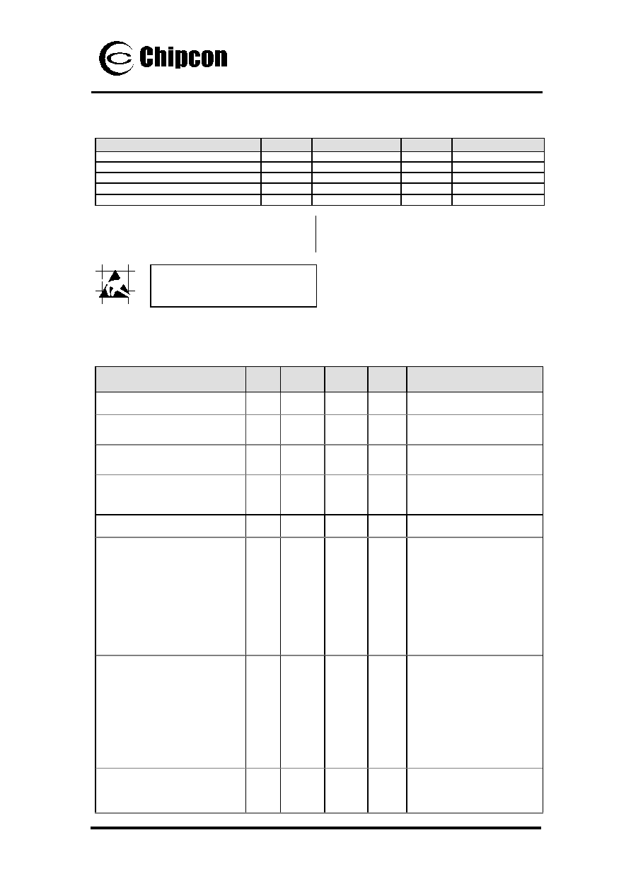
Absolute Maximum Ratings
Parameter
Min.
Max.
Units
Condition
Supply voltage, VDD
-0.3
5.0
V
Voltage on any pin
-0.3
VDD+0.3, max 5.0
V
Input RF level
10
dBm
Storage temperature range
-50
150
∞C
Reflow soldering temperature
260
∞C
T = 10 s
The absolute maximum ratings given
above should under no circumstances be
violated. Stress exceeding one or more of
the limiting values may cause permanent
damage to the device.
Caution!
ESD sensitive device.
Precaution should be used when handling
the device in order to prevent permanent
damage.
Electrical Specifications
Tc = 25
∞C, AVDD = DVDD = 3.0 V if nothing else stated. Crystal frequency = 14.7456 MHz.
All measurements were performed using the test circuit shown in Figure 3.
Parameter
Min.
Typ.
Max.
Unit
Condition / Note
Overall
RF Frequency Range
402
804
470
940
MHz
MHz
Programmable in <300 Hz steps
Programmable in <600 Hz steps
Operating ambient temperature
range
-40 85
∞C
Supply voltage
2.3 3.0 3.6 V
Note: The same supply voltage
should be used for digital (DVDD)
and analogue (AVDD) power.
Transmit Section
Transmit data rate
0.45
153.6
kBaud
Data rate is programmable. See
"Data rate programming" on page
27 for details.
NRZ or Manchester encoding can
be used. 153.6 kBaud equals
153.6 kbps using NRZ coding.
See page 21.
Minimum data rate for OOK/ASK
is 2.4 kBaud
Binary FSK frequency separation
0
0
108
216
kHz
kHz
in 402 - 470 MHz range
in 804 - 940 MHz range
The frequency separation is
programmable in 250 Hz steps.
108/216 kHz is the maximum
guaranteed separation at 1.84
MHz reference frequency. Larger
separations can be achieved at
higher reference frequencies.
Output power
433 MHz
868 MHz
-20
-20
10
5
dBm
dBm
Delivered to 50
load.
The output power is
programmable.
Chipcon AS
SmartRF
Æ
CC1020 Datasheet (rev. 1.4), 2003-11-18
Page 4 of 83

SmartRF
Æ
CC1020
Parameter
Min.
Typ.
Max.
Unit
Condition / Note
Output power tolerance
-4
3
dB
dB
At maximum output power
At 2.3 V, +85
o
C
At 3.6 V, -40
o
C
Harmonics
2
nd
harmonic, 433 MHz, +10 dBm
3
rd
harmonic, 433 MHz, +10 dBm
2
nd
harmonic, 868 MHz, +5 dBm
3
rd
harmonic, 868 MHz, +5 dBm
-60
-65
-54
-60
dBc
dBc
dBc
dBc
An external LC Filter is used to
suppress harmonics.
Adjacent channel power (GFSK)
12.5 kHz channel width, 426 MHz
25 kHz channel width, 868 MHz
-46
-51
dBc
dBc
ACP is measured in a ±4.25 and
±8.5 kHz bandwidth at 12.5 and
25 kHz offsets for 12.5 and 25
kHz channel widths respectively.
Modulation for 12.5/25 kHz
channel width: 2.4/4.8 kBaud
NRZ PN9 sequence, ±2.0/2.4
kHz frequency deviation.
Occupied bandwidth (99.5%,GFSK)
12.5 kHz channel width, 426 MHz
25 kHz channel width, 868 MHz
7
9
kHz
kHz
Bandwidth for 99.5% of total
average power. Modulation for
12.5/25 kHz channel width:
2.4/4.8 kBaud NRZ PN9
sequence, ±2.0/2.4 kHz
frequency deviation.
Spurious emission
47-74, 87.5-118,
174-230, 470-862 MHz
9 kHz ≠ 1 GHz
1 ≠ 4 GHz
-54
-36
-30
dBm
dBm
dBm
10/5 dBm at 433/868 MHz
Modulation is 2.4 kBaud,
Manchester coded data, ±2.0 kHz
frequency deviation. An external
LC filter must be used to reduce
out-of-band spurs.
Complying with EN 300 220,
FCC CFR47 part 15 and ARIB
STD T-67.
Optimum load impedance
434 MHz
868 MHz
915 MHz
57 + j106
36 + j74
57 + j76
Transmit mode, series equivalent.
For matching details see "Input/
output matching" on page 53.
Optimum load admittance
434 MHz
868 MHz
915 MHz
250
||
50 nH
180
||
17 nH
160
||
20 nH
Transmit mode, parallel
equivalent. For matching details
see "Input/ output matching" on
page 53.
Chipcon AS
SmartRF
Æ
CC1020 Datasheet (rev. 1.4), 2003-11-18
Page 5 of 83