 | –≠–ª–µ–∫—Ç—Ä–æ–Ω–Ω—ã–π –∫–æ–º–ø–æ–Ω–µ–Ω—Ç: CC1070SK | –°–∫–∞—á–∞—Ç—å:  PDF PDF  ZIP ZIP |

SmartRF
Æ
CC1070
CC1070
Single Chip Low Power RF Transmitter for
Narrow Band Systems
Applications
∑ Narrow-band low power UHF wireless
data transmitters
∑
402 / 426 / 429 / 433 / 868 and 915
MHz ISM/SRD band systems
∑
TPMS ≠ Tire Pressure Monitoring
Systems
∑ AMR ≠ Automatic Meter Reading
∑ Wireless alarm and security systems
∑ Home automation
∑ Low power telemetry
Product Description
CC1070 is a true single-chip UHF
transmitter designed for very low power
and very low voltage wireless applications.
The circuit is mainly intended for the ISM
(Industrial, Scientific and Medical) and
SRD (Short Range Device) frequency
bands at 402, 426, 429, 433, 868 and 915
MHz, but can easily be programmed for
multi-channel operation at other
frequencies in the 402 - 470 and 804 - 940
MHz range.
The
CC1070 is especially suited for narrow-
band systems, e.g. with channel widths of
12.5 or 25 kHz complying with ARIB STD
T-67 and EN 300 220.
The
CC1070 main operating parameters
can be programmed via an easy-to-
interface serial bus, thus making
CC1070 a
very flexible and easy to use transmitter.
In a typical application
CC1070 will be used
together with a microcontroller and a few
external passive components.
CC1070 is based on Chipcon's SmartRF
Æ
-
02 technology in 0.35
µm CMOS.
Features
∑ True single chip UHF RF transmitter
∑ Frequency range 402 - 470 MHz and
804 - 940 MHz
∑ Programmable output power
∑ Low supply voltage (2.1 to 3.6 V)
∑ Very few external components required
∑ Small size (QFN 20 package)
∑ Data rate up to 153.6 kBaud
∑ ASK, FSK and GFSK data modulation
∑ Fully on-chip VCO
∑ Programmable frequency make crystal
temperature drift compensation
possible without TCXO
∑ Suitable for frequency hopping systems
∑ Complies with EN 300 220, FCC
CFR47 part 15 and ARIB STD T-67
∑ Development kit available
∑ Easy-to-use software for generating the
CC1070 configuration data
Chipcon AS SmartRF
Æ
CC1070 PRELIMINARY DATASHEET (rev. 1.0), 2003-10-30
Page 1 of 45

SmartRF
Æ
CC1070
Table of Contents
Single Chip Low Power RF Transmitter for Narrow Band Systems....................................................1
Applications........................................................................................................................................1
Product Description............................................................................................................................1
Features.............................................................................................................................................1
Table of Contents...............................................................................................................................2
Absolute Maximum Ratings ...............................................................................................................3
Electrical Specifications .....................................................................................................................3
Pin Assignment ..................................................................................................................................7
Circuit Description..............................................................................................................................8
Application Circuit ..............................................................................................................................8
Configuration Overview....................................................................................................................11
Configuration Software.....................................................................................................................11
Microcontroller Interface...................................................................................................................12
4-wire Serial Configuration Interface ................................................................................................13
Signal Interface ................................................................................................................................15
Built-in Test Pattern Generator ........................................................................................................17
FSK Modulation Formats .................................................................................................................17
OOK/ASK Modulation ......................................................................................................................17
Data Rate Programming ..................................................................................................................17
Interrupt upon PLL Lock...................................................................................................................18
Interfacing an External PA ...............................................................................................................18
General Purpose Output Control Pins..............................................................................................19
Frequency Programming..................................................................................................................19
Dithering...........................................................................................................................................20
VCO, Charge Pump and PLL Loop Filter .........................................................................................20
VCO and PLL Self-Calibration .........................................................................................................21
VCO Current Control........................................................................................................................22
Power Management .........................................................................................................................23
Output Power Programming.............................................................................................................25
Crystal Oscillator..............................................................................................................................26
Output Matching...............................................................................................................................27
Optional LC Filter .............................................................................................................................27
System Considerations and Guidelines ...........................................................................................28
PCB Layout Recommendations .......................................................................................................29
Antenna Considerations...................................................................................................................30
Configuration Registers....................................................................................................................30
CC1070 Register Overview..............................................................................................................31
Package Description (QFN 20) ........................................................................................................42
Package Thermal Properties............................................................................................................43
Soldering Information .......................................................................................................................43
Tray Specification ............................................................................................................................43
Carrier Tape and Reel Specification ................................................................................................43
Ordering Information ........................................................................................................................43
General Information .........................................................................................................................44
Address Information.........................................................................................................................45
Chipcon AS SmartRF
Æ
CC1070 PRELIMINARY DATASHEET (rev. 1.0), 2003-10-30
Page 2 of 45
SmartRF
Æ
CC1070
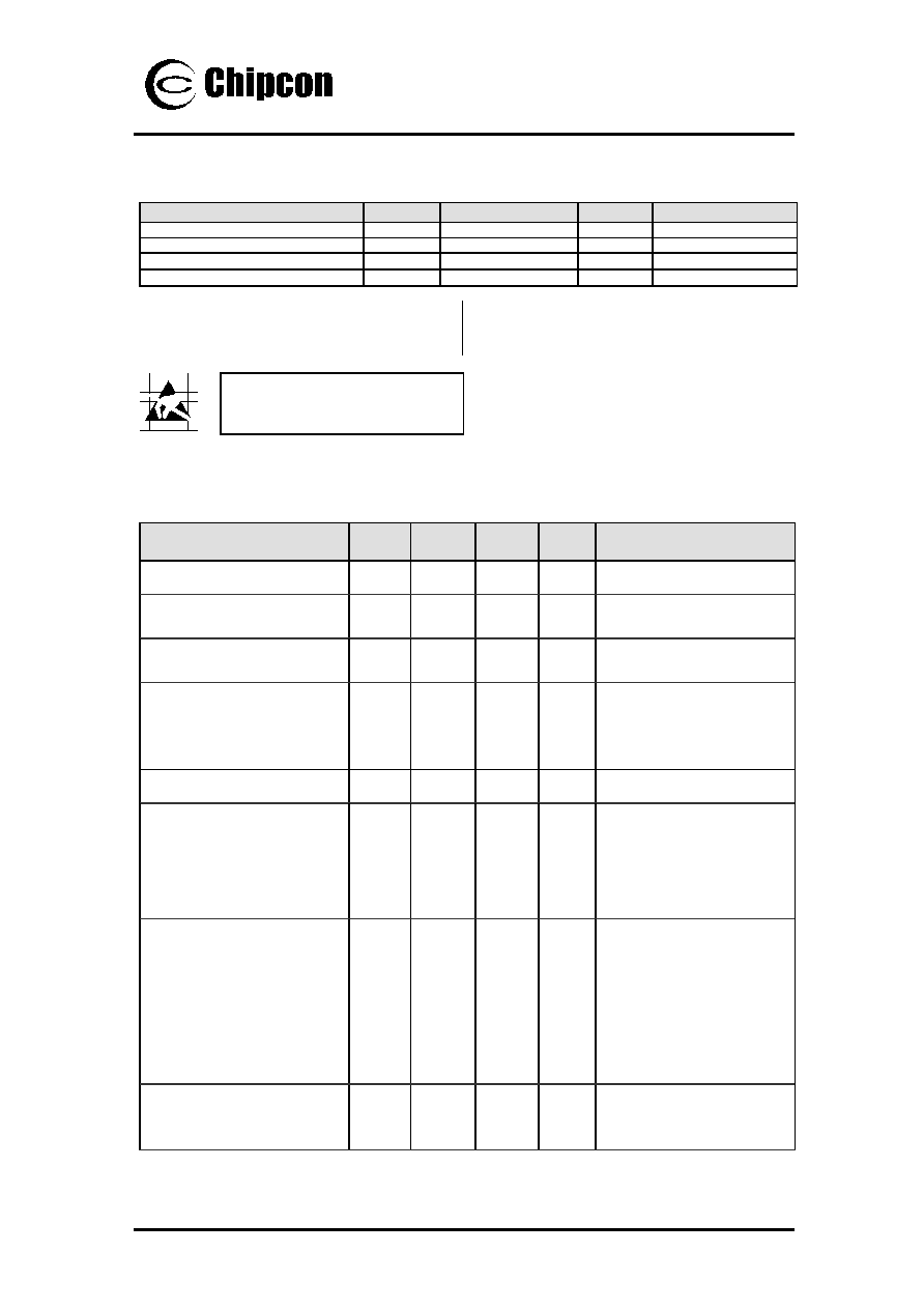
Absolute Maximum Ratings
Parameter
Min.
Max.
Units
Condition
Supply voltage, VDD
-0.3 5.0 V
Voltage on any pin
-0.3
VDD+0.3, max 5.0
V
Storage temperature range
-50 150
∞C
Reflow soldering temperature
260
∞C
T = 10 s
The absolute maximum ratings given
above should under no circumstances be
violated. Stress exceeding one or more of
the limiting values may cause permanent
damage to the device.
Caution!
ESD sensitive device.
Precaution should be used when handling
the device in order to prevent permanent
damage.
Electrical Specifications
Tc = 25
∞C, DVDD = AVDD = 3.0 V if nothing else stated. Crystal frequency = 14.7456 MHz
All measurements were performed using the test circuit shown in Figure 3.
Parameter
Min.
Typ.
Max.
Unit
Condition / Note
Overall
RF Frequency Range
402
804
470
940
MHz
MHz
Programmable in <300 Hz steps
Programmable in <600 Hz steps
Operating ambient temperature
range
-40 105
∞C
Supply voltage
2.1
3.0
3.6
V
Recommended operation voltage.
Note: The same supply voltage
should be used for digital (DVDD)
and analog (AVDD) power.
Transmit Section
Transmit data rate
0.45
153.6
kBaud
Data rate is programmable. See
"Data rate programming" on page
17 for details.
NRZ or Manchester encoding can
be used. 153.6 kBaud equals
153.6 kbps using NRZ coding.
Binary FSK frequency separation
0
0
108
216
kHz
kHz
in 402 - 470 MHz
in 804 - 940 MHz
The frequency separation is
programmable in 250 Hz steps.
108/216 kHz is the maximum
guaranteed separation at 1.84
MHz reference frequency. Larger
separations can be achieved at
higher reference frequencies.
Output power
433 MHz
868 MHz
-20
-20
10
8
dBm
dBm
Delivered to 50
load.
The output power is
programmable.
Chipcon AS SmartRF
Æ
CC1070 PRELIMINARY DATASHEET (rev. 1.0), 2003-10-30
Page 3 of 45

SmartRF
Æ
CC1070
Parameter
Min.
Typ.
Max.
Unit
Condition / Note
Harmonics
2
nd
harmonic, 433 MHz, +10 dBm
3
rd
harmonic, 433 MHz, +10 dBm
2
nd
harmonic, 868 MHz, +8 dBm
3
rd
harmonic, 868 MHz, +8 dBm
-55
-64
-50
-57
dBc
dBc
At maximum output power. An
external LC filter is used to
reduce harmonic emissions
Adjacent channel power (GFSK)
12.5 kHz channel width, 426 MHz
25 kHz channel width, 868 MHz
-47
-50
dBc
dBc
ACP is measured in a ±4.25 and
±8.5 kHz bandwidth at 12.5 and
25 kHz offsets for 12.5 and 25
kHz channel widths respectively.
Modulation for 12.5/25 kHz
channel width: 2.4/4.8 kBaud
NRZ PN9 sequence, ±2.0/2.4 kHz
frequency deviation.
Occupied bandwidth (99.5%,GFSK)
12.5 kHz channel width, 426 MHz
25 kHz channel width, 868 MHz
7
10
kHz
kHz
Bandwidth for 99.5% of total
average power. Modulation for
12.5/25 kHz channel width:
2.4/4.8 kBaud NRZ PN9
sequence, ±2.0/2.4 kHz
frequency deviation.
Spurious emission
47-74, 87.5-118,
174-230,470-862 MHz
9 kHz ≠ 1 GHz
1 ≠ 4 GHz
-54
-36
-30
dBm
dBm
dBm
Maximum output power.
Modulation is 2.4 kBaud,
Manchester coded data, ±2.0 kHz
frequency deviation. An external
LC filter must be used to reduce
out-of-band spurs.
Optimum load impedance
433 MHz
868 MHz
915 MHz
TBD
TBD
TBD
Transmit mode, series equivalent.
For matching details see "Output
matching details" page 27.
Frequency Synthesizer
Section
Crystal Oscillator Frequency
4 14.7456 20 MHz
Crystal operation
Parallel
C4 and C5 are loading
capacitors. See page 26.
Crystal load capacitance
12
12
12
22
16
16
30
30
16
pF
pF
pF
4-6 MHz, 22 pF recommended
6-8 MHz, 16 pF recommended
8-20 MHz, 16 pF recommended
Crystal oscillator start-up time
1.55
0.90
0.95
0.63
ms
ms
ms
ms
4.9152 MHz, 12 pF load
9.8304 MHz, 12 pF load
14.7456 MHz, 16 pF load
19.6608 MHz, 12 pF load
External clock signal drive, sine
wave
300
mVpp
The external clock signal must be
connected to XOSC_Q1 using a
DC block (10 nF). Set
XOSC_BYPASS = 0 in the
INTERFACE register when using
an external clock signal with low
amplitude or a crystal.
A full-swing digital external clock
can also be used, with no DC
block capacitor. In that case, set
XOSC_BYPASS = 1.
See page 26 for further details.
Chipcon AS SmartRF
Æ
CC1070 PRELIMINARY DATASHEET (rev. 1.0), 2003-10-30
Page 4 of 45

SmartRF
Æ
CC1070
Parameter
Min.
Typ.
Max.
Unit
Condition / Note
Reference frequency accuracy
requirement
+/-
5.7
+/- 2.8
+/- 4
+/- 7
ppm
ppm
ppm
ppm
433 MHz (EN 300 220)
868 MHz (EN 300 220)
Must be less than ±5.7 / ±2.8
ppm to comply with EN 300 220
25 kHz channel width at 433/868
MHz.
Must be less than ±4 ppm to
comply with Japanese 12.5 kHz
channel width regulations (ARIB
STD T-67). NOTE: This imposes
special requirements on the
receiver of the signal.
Must be less than ±7 ppm to
comply with Korean 12.5 kHz
channel width regulations. NOTE:
This imposes special
requirements on the receiver of
the signal.
NOTE:
The reference frequency
accuracy (initial tolerance) and
drift (aging and temperature
dependency) will determine the
frequency accuracy of the
transmitted signal.
Crystal oscillator temperature
compensation can be done using
the fine frequency
programmability.
Phase noise, 402 ≠ 470 MHz
12.5 kHz channel width
-87
-95
-100
-105
-114
dBc/Hz
dBc/Hz
dBc/Hz
dBc/Hz
dBc/Hz
Unmodulated carrier
At 12.5 kHz offset from carrier
At 25 kHz offset from carrier
At 50 kHz offset from carrier
At 100 kHz offset from carrier
At 1 MHz offset from carrier
Measured using loop filter
components given in Table 3.
The phase noise will be higher for
larger PLL loop filter bandwidth.
Phase noise, 804 - 940 MHz
25 kHz channel width
-81
-89
-96
-103
-122
dBc/Hz
dBc/Hz
dBc/Hz
dBc/Hz
dBc/Hz
Unmodulated carrier
At 12.5 kHz offset from carrier
At 25 kHz offset from carrier
At 50 kHz offset from carrier
At 100 kHz offset from carrier
At 1 MHz offset from carrier
Measured using loop filter
components given in Table 3.
The phase noise will be higher for
larger PLL loop filter bandwidth.
PLL loop bandwidth
12.5 kHz channel width, 433 MHz
25 kHz channel width, 868 MHz
TBD
7
kHz
kHz
After PLL and VCO calibration.
The PLL loop bandwidth is
programmable
Digital Inputs/Outputs
Logic "0" input voltage
0
0.3*VDD
V
Logic "1" input voltage
0.7*VDD
VDD
V
Chipcon AS SmartRF
Æ
CC1070 PRELIMINARY DATASHEET (rev. 1.0), 2003-10-30
Page 5 of 45