 | –≠–ª–µ–∫—Ç—Ä–æ–Ω–Ω—ã–π –∫–æ–º–ø–æ–Ω–µ–Ω—Ç: CC900 | –°–∫–∞—á–∞—Ç—å:  PDF PDF  ZIP ZIP |
SmartRF
SmartRF
SmartRF
SmartRF
CC900
Chipcon AS
SmartRF
CC900 Datasheet (rev. 2.0) 2003-05-14
Page 1 of 27
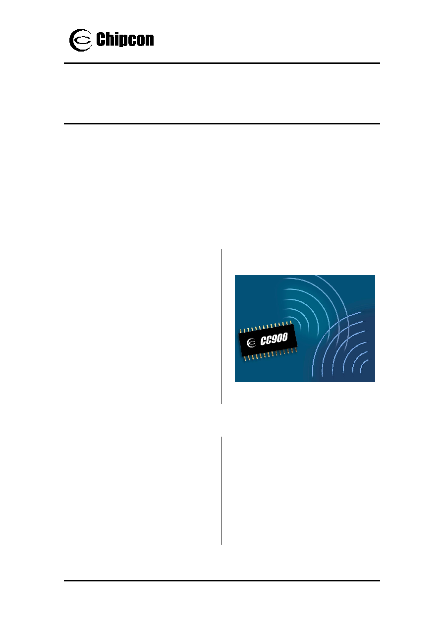
CC900
Single Chip High Performance RF Transceiver
Applications
∑ UHF wireless data transmitters and
receivers
∑ Wireless alarm and security systems
∑ 868 and 915 MHz ISM/SRD band
systems
∑ Keyless entry with acknowledgement
∑ Remote control systems
∑ Home security and automation
∑ Low power telemetry
∑ Remote metering
∑ Environmental control
∑ Social alarms
Product Description
CC900
is a single-chip high performance
UHF transceiver designed for low-power
and low-voltage wireless applications. The
circuit is mainly intended for the ISM
(Industrial, Scientific and Medical) and
SRD (Short Range Device) frequency
bands at 868 and 915 MHz, but can easily
be programmed for operation at other
frequency bands in the 800-1000 MHz
range.
The main operating parameters of
CC900
can be programmed via a serial interface,
thus making
CC900
a very flexible and
easy to use transceiver. In a typical system
CC900
will be used together with a
microcontroller and a few external passive
components.
CC900
is based on Chipcon's SmartRF
technology.
Features
∑ Single chip UHF RF transceiver
∑ Frequency range 800 ≠ 1000 MHz
∑ High sensitivity (typical -110 dBm)
∑ Programmable output power up to
4 dBm
∑ Complies with EN 300 220
∑ Small size (SSOP-28 package)
∑ Low supply voltage (2.7 V to 3.3 V)
∑ Very few external components required
∑ No external RF switch required
∑ No external IF filter required
∑ Single port antenna connection
∑ FSK modulation with data-rate up to 9.6
kbit/s
∑ Suitable for both narrow and wide band
systems
∑ Radio frequency (RF) programmable in
steps of 250 Hz makes crystal temp-
erature drift compensation possible
∑ Suitable for frequency hopping
protocols
∑ Development kit available
∑ Easy-to-use software for generating the
CC900
configuration data

SmartRF
SmartRF
SmartRF
SmartRF
CC900
Chipcon AS
SmartRF
CC900 Datasheet (rev. 2.0) 2003-05-14
Page 2 of 27
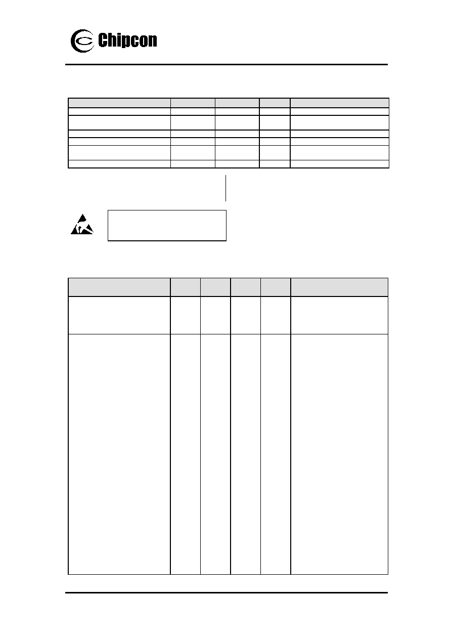
Pin Assignment
Pin no.
Pin name
Pin type
Description
1
AVDD
Power (A)
Power supply (3 V) for analog modules
2
AGND
Ground (A)
Ground connection (0 V) for analog modules
3
AGND
Ground (A)
Ground connection (0 V) for analog modules
4
AGND
Ground (A)
Ground connection (0 V) for analog modules
5
AGND
Ground (A)
Ground connection (0 V) for analog modules
6
RF_IN
RF Input
RF signal input from antenna (external ac-coupling)
7
RF_OUT
RF output
RF signal output to antenna
8
AVDD
Power (A)
Power supply (3 V) for analog modules
9
AVDD
Power (A)
Power supply (3 V) for analog modules
10
VCO_IN
Analog input
External VCO-tank input
11
AGND
Ground (A)
Ground connection (0 V) for analog modules
12
CHP_OUT
Analog output
Charge pump current output
13
AVDD
Power (A)
Power supply (3 V) for analog modules
14
AVDD
Power (A)
Power supply (3 V) for analog modules
15
XOSC_Q1
Analog input
Crystal, pin 1, or external clock input
16
XOSC_Q2
Analog output
Crystal, pin 2
17
AGND
Ground (A)
Ground connection (0 V) for analog modules
18
DGND
Ground (D)
Ground connection (0 V) for digital modules
19
LOCK
Digital output
PLL Lock indicator. Output is high when PLL is in lock
20
DGND
Ground (D)
Ground connection (0 V) for digital modules
21
DVDD
Power (D)
Power supply (3 V) for digital modules
22
DVDD
Power (D)
Power supply (3 V) for digital modules
23 DIO
Digital
input/output
(bidirectional)
Data input in transmit mode
Demodulator output in receive mode
24
CLOCK
Digital input
Programming clock for 3-wire bus
25
PDATA
Digital input
Programming data for 3-wire bus
26
STROBE
Digital input
Programming strobe (Load) for 3-wire bus
27
IF_IN
Analog input
Input to IF chain (from optional external ceramic filter). The input
impedance is 1.5 k
so a direct connection to an external ceramic
filter is possible
28
IF_OUT
Analog output
Output from first amplifier in IF-chain (to optional external ceramic
filter). The output impedance is 1.5 k
so a direct connection to
an external ceramic filter is possible
A=Analog, D=Digital
(Top view)
1
14
15
AVDD
AGND
AGND
AGND
RF_IN
RF_OUT
AVDD
AVDD
VCO_IN
AGND
AVDD
CHP_OUT
AVDD
2
3
4
6
5
7
8
9
11
12
13
10
28
IF_OUT
IF_IN
STROBE
PDATA
CLOCK
DIO
DVDD
DVDD
DGND
LOCK
DGND
XOSC_Q2
AGND
XOSC_Q1
27
26
25
23
24
22
21
20
18
17
16
19
AGND
CC9
00
SmartRF
SmartRF
SmartRF
SmartRF
CC900
Chipcon AS
SmartRF
CC900 Datasheet (rev. 2.0) 2003-05-14
Page 3 of 27
Absolute Maximum Ratings
Parameter
Min.
Max.
Units
Condition
Supply voltage, VDD
-0.3
7.0
V
Voltage on any pin
-0.3
VDD+0.3,
max 7.0
V
Input RF level
10
dBm
Storage temperature range
-50
150
∞C
Operating ambient temperature
range
-30 85
∞C
Lead temperature
260
∞C
T = 10 s
Under no circumstances the absolute
maximum ratings given above should be
violated. Stress exceeding one or more of
the limiting values may cause permanent
damage to the device.
Caution! ESD sensitive device.
Precaution should be used when handling
the device in order to prevent permanent
damage.
Electrical Specifications
Parameter
Min.
Typ.
Max.
Unit
Condition
Overall
RF Frequency Range
800
868
1000
MHz
Programmable in steps of 250 Hz
Transmit Section
Transmit data rate
0.3 2.4 9.6 kbit/s
Manchester
code
is
required.
(9.6 kbit/s equals 19.2 kbaud/s
using Manchester code)
Binary FSK frequency separation
0
10
200
kHz
The frequency corresponding to
the digital "0" is denoted f
0
, while
f
1
corresponds to a digital "1".
The frequency separation is f
1
-f
0
.
The RF carrier frequency, f
c
, is
then given by f
c
=(f
0
+f
1
)/2.
(The frequency deviation is given
by f
d
=+/-(f
1
-f
0
)/2 )
The frequency separation is
programmable.
Programmable output power
-20 4
dBm
Delivered
to
50
load.
The output power is
programmable in steps of 1 dB.
RF output impedance
200
Transmit mode, parallel
equivalent. For matching details
see "Input/ output matching" p.
13.
Harmonics
-25
dBc
When using a high output power
level an external LC or SAW filter
may be used to reduce
harmonics emission to comply
with SRD requirements. See p.14

SmartRF
SmartRF
SmartRF
SmartRF
CC900
Chipcon AS
SmartRF
CC900 Datasheet (rev. 2.0) 2003-05-14
Page 4 of 27
Parameter
Min.
Typ.
Max.
Unit
Condition
Receive Section
Receiver Sensitivity
-110
dBm
Measured at a data rate of 1.2
kbit/s, 60 kHz IF and 20 kHz
frequency separation with a bit
error rate better than 10
-3
. For
other settings see p. 12.
Cascaded noise figure
3
dB
LO leakage
-57
dBm
Depends on external components
placement
Input impedance
16
3.6 pF
Receive mode, series equivalent
at 869 MHz.
For matching details see "Input/
output matching" p.13.
Turn on time
500
3
5
30
µs
ms
ms
ms
With precharging, 9.6 kbit/s
Without precharging, 9.6 kbit/s
With precharging, 1.2 kbit/s
Without precharging, 1.2 kbit/s
See "Demodulator precharging
for reduced turn-on time" p.18.
Blocking / Desensitization
±1 MHz
±2 MHz
±5 MHz
30
35
50
dB
dB
dB
See p. 15 for details.
Using an external SAW filter at
the front end will improve the
blocking performance
IF Section
Intermediate frequency (IF)
60
200
455
kHz
kHz
kHz
The IF is programmable. Either
60 kHz, 200 kHz or 455 kHz can
be chosen
An optional external IF filter can
be used if 455 kHz is chosen.
The impedance level is 1.5 k
Frequency Synthesiser
Section
Crystal Oscillator Frequency
4 12 13
MHz
Crystal frequency accuracy
requirement
+/-
50
ppm
The crystal frequency accuracy
and drift (ageing and
temperature dependency) will
determine the frequency
accuracy of the transmitted
signal.
Crystal operation
Parallel
C151 and C161 are loading
capacitors, see p. 14.
Crystal load capacitance
20
16
12
pF
pF
pF
4-6 MHz
6-10 MHz
10-13 MHz
Crystal oscillator start-up time
3
6
ms
12 MHz, 12 pF load
Output signal phase noise
-90
dBc/Hz
100
kHz
offset
from
carrier
PLL lock time (RX / TX turn time)
100 µs
SmartRF
SmartRF
SmartRF
SmartRF
CC900
Chipcon AS
SmartRF
CC900 Datasheet (rev. 2.0) 2003-05-14
Page 5 of 27
Parameter
Min.
Typ.
Max.
Unit
Condition
PLL turn-on time, crystal oscillator
off in power down mode
4 ms
PLL turn-on time, crystal oscillator
on in power down mode
2 ms
Digital Inputs/Outputs
Logic "0" input voltage
0
0.3*VDD
V
Logic "1" input voltage
0.7*VDD
VDD V
Logic "0" output voltage
0
0.4
V
Output current -2.5 mA,
3.0 V supply voltage
Logic "1" output voltage
2.5
VDD
V
Output current 2.5 mA,
3.0 V supply voltage
Logic "0" input current
NA -1 µA
Input signal equals GND
Logic "1" input current
NA 1 µA
Input signal equals VDD
Power Supply
Supply voltage
2.7
3.0
3.3
V
V
Recommended operation voltage
Operating limits
Current Consumption,
receive mode
21 mA
Current Consumption,
average in receive mode using
polling
210 µA
1:100 receive to power down ratio
Current Consumption,
transmit mode:
P=0.01 mW (-20 dBm)
P=0.1 mW (-10 dBm)
P=1 mW (0 dBm)
P=2.5 mW (4 dBm)
25
31
54
91
mA
mA
mA
mA
The ouput power is delivered to a
50
load
Current Consumption,
Power Down
30
0.2
1
µA
µA
Oscillator core on
Oscillator core off