 | –≠–ª–µ–∫—Ç—Ä–æ–Ω–Ω—ã–π –∫–æ–º–ø–æ–Ω–µ–Ω—Ç: CH7004C-T | –°–∫–∞—á–∞—Ç—å:  PDF PDF  ZIP ZIP |

201-0000-024 Rev 2.1, 8/2/99
1
CH7004C
CHRONTEL
Digital PC to TV Encoder with Macrovision
TM
Features
∑ Supports Macrovision
TM
7.X anti-copy protection
∑ Pin and function compatible with CH7003
∑ Universal digital interface accepts YCrCb (CCIR601
or 656) or RGB (15, 16 or 24-bit) video data in both
non-interlaced and interlaced formats
∑ True Scale
TM
rendering engine supports undescan
operations for various graphics resolutions
•
∑ Enhanced text sharpness and adaptive flicker removal
with up to 5-lines of filtering
∑ Enhanced dot crawl control and area reduction
∑ Fully programmable through I
2
C port
∑ Supports NTSC, NTSC-EIA (Japan), and PAL (B, D,
G, H, I, M and N) TV formats
∑ Provides Composite, S-Video and SCART outputs
∑ Auto-detection of TV presence
∑ Supports VBI pass-through
∑ Programmable power management
∑ 9-bit video DAC outputs
∑ Complete Windows and DOS driver software
∑ Offered in 44-pin PLCC, 44-pin TQFP, or 100-pin
PQFP package options
∑ 4 Programmable GPIO pins (only with 100-pin PQFP)
General Description
Chrontel's CH7004 digital PC to TV encoder is a stand-
alone integrated circuit which provides a PC 99 compliant
solution for TV output. It provides a universal digital input
port to accept a pixel data stream from a compatible VGA
controller (or equivalent) and converts this directly into
NTSC or PAL TV format.
This circuit integrates a digital NTSC/PAL encoder with
9-bit DAC interface, and new adaptive flicker filter, and
high accuracy low-jitter phase locked loop to create
outstanding quality video. Through its TrueScale
TM
scaling and de-flickering engine, the CH7004 supports full
vertical and horizontal underscan capability and operates
in 5 different resolutions including 640x480 and 800x600.
A new universal digital interface along with full
programmability make the CH7004 ideal for system-level
PC solutions. All features are software programmable
through a standard I
2
C port, to enable a complete PC
solution using a TV as the primary display.
Patent number 5,781,241
•
Patent number 5,914,753
Figure 1: Functional Block Diagram
TRIPLE
DAC
PLL
RGB-YUV
CONVERTER
SYSTEM CLOCK
Y/R
CVBS/B
C/G
YUV-RGB CONVERTER
DIGITAL
INPUT
INTERFACE
I
2
C REGISTER & CONTROL
BLOCK
LINE
MEMORY
TRUE SCALE
SCALING & DEFLICKERING
ENGINE
TIMING & SYNC GENERATOR
NTSC/PAL
ENCODER
& FILTERS
D[15:0]
PIXEL DATA
XCLK
H
V
XI XO/FIN
P-OUT
SC
SD
ADDR
BCO
RSET
CSYNC
CHRONTEL
CH7004C
2
201-0000-024 Rev 2.1, 8/2/99
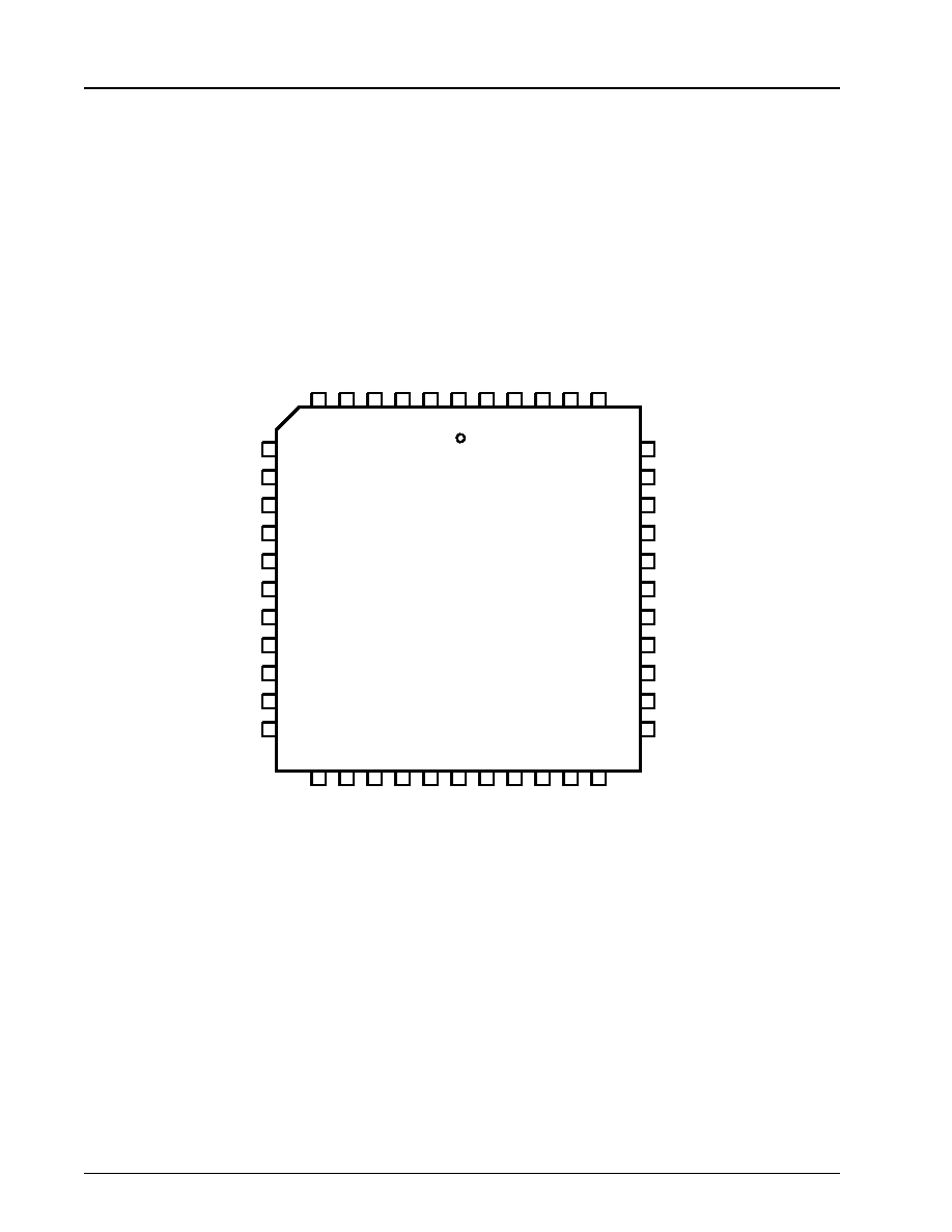
Figure 2: 44-Pin PLCC
XO/FIN
XI
DVDD
ADDR
D[3]
D[4]
D[5]
D[8]
D[6]
DVDD
D[7]
DGND
SC
SD
DGND]
D[9]
D[10]
D[11]
AVDD
VDD
RSET
GND
D
[
2
]
D
[
1
]
V
H
X
C
L
K
D
V
D
D
P
-
O
U
T
D
[
0
]
D
G
N
D
B
C
O
A
G
N
D
D
[
1
2
]
D
[
1
3
]
D
[
1
4
]
D
G
N
D
D
[
1
5
]
D
V
D
D
C
S
Y
N
C
G
N
D
C
V
B
S
C
Y
7
8
9
10
13
12
11
39
38
37
36
35
14
15
16
17
34
33
32
31
30
29
6
5
4
3
2
1
4
4
4
3
4
2
4
1
4
0
1
8
1
9
2
0
2
1
2
4
2
3
2
2
2
5
2
6
2
7
2
8
CHRONTEL
CH7004
CHRONTEL
CH7004C
201-0000-024 Rev 2.1, 8/2/99
3
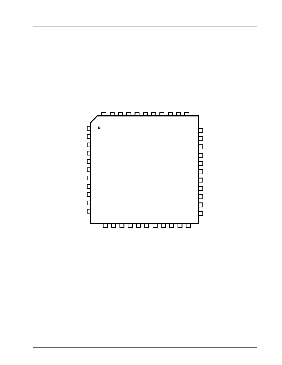
Figure 3: 44-PIN TQFP
XO/FIN
XI
DVDD
ADDR
D[3]
D[4]
D[5]
D[8]
D[6]
DVDD
D[7]
DGND
SC
SD
DGND]
D[9]
D[10]
D[11]
AVDD
VDD
RSET
GND
D
[
2
]
D
[
1
]
V
H
X
C
L
K
D
V
D
D
P
-
O
U
T
D
[
0
]
D
G
N
D
B
C
O
A
G
N
D
D
[
1
2
]
D
[
1
3
]
D
[
1
4
]
D
G
N
D
D
[
1
5
]
D
V
D
D
C
S
Y
N
C
G
N
D
C
V
B
S
C
Y
1
2
3
4
7
6
5
33
32
31
30
29
8
9
10
11
28
27
26
25
24
23
4
4
4
3
4
2
4
1
4
0
3
9
3
8
3
7
3
6
3
5
3
4
1
3
1
3
1
4
1
5
1
8
1
7
1
6
1
9
2
0
2
1
2
2
CHRONTEL
CH7004
D[3]
D[4]
D[5]
D[8]
D[6]
DVDD
D[7]
DGND]
D[9]
D[10]
D[11]
XO/FIN
XI
DVDD
ADDR
DGND
SC
SD
AVDD
VDD
RSET
GND

CHRONTEL
CH7004C
4
201-0000-024 Rev 2.1, 8/2/99
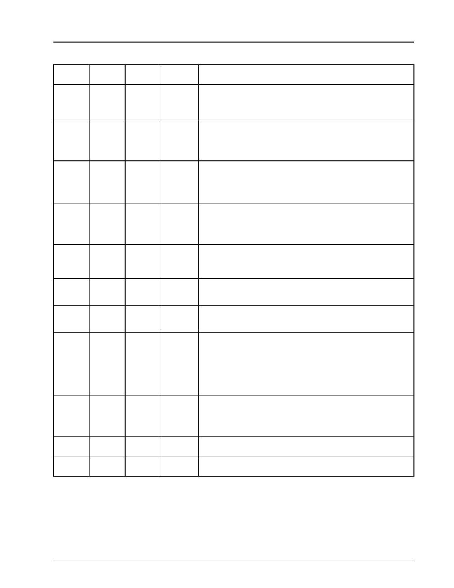
Table 1. Pin Descriptions
44-Pin
PLCC
44Pin
TQFP
Type
Symbol
Description
21-15
13-12,
10-4
15,14,
13,12,
11,10,
9,7,6,
4,3,
2,1,
44,43,42
In
D15-D0
Digital Pixel Inputs
These pins accept digital pixel data streams with either 8, 12, or 16-bit
multiplexed or 16-bit non-multiplexed formats, determined by the input
mode setting (see Registers and Programming section). Inputs D0 - D7
are used when operating in 8-bit multiplexed mode. Inputs D0 - D11 are
used when operating in 12-bit mode. Inputs D0 - D15 are used when
operating in 16-bit mode. The data structure and timing sequence for
each mode is described in the section on Digital Input Port.
43
37
Out
P-OUT
Pixel Clock Output
The CH7004, operating in master mode, provides a pixel data clocking
signal to the VGA controller. This pin provides the pixel clock output
signal (adjustable as X, 2X or 3X) to the VGA controller (see the section
on Digital Video Interface and Registers and Programming for more
details). The capacitive loading on this pin should be kept to a
minimum.
1
39
In
XCLK
Pixel Clock Input
To operate in a pure master mode, the P-OUT signal should be
connected to the XCLK input pin. To operate in a pseudo-master mode,
the P-OUT clock is used as a reference frequency, and a signal locked
to this output (at 1X, 1/2X, or 1/3X the P-OUT frequency) is input to the
XCLK pin. To operate in slave mode, the CH7004 accepts an external
pixel clock input at this pin. The capacitive loading on this pin should be
kept to a minimum.
3
41
In/Out
V
Vertical Sync Input/Output
This pin accepts the vertical sync signal from the VGA controller, or
outputs a vertical sync to the VGA controller. The capacitive loading on
this pin should kept to a minimum.
2
40
In/Out
H
Horizontal Sync Input/Output
This pin accepts the horizontal sync from the VGA controller, or outputs
a horizontal sync to the VGA controller. The capacitive loading on this
pin should be kept to a minimum.
41
35
Out
BCO
Buffered Clock Output
This pin provides a buffered output of the 14.31818 MHz crystal input
frequency for other devices and remains active at all times (including
power-down). The output can also be selected to be other frequencies
(see Registers and Programming).
38
32
In
XI
Crystal Input
A parallel resonance 14.31818 MHz (± 50 ppm) crystal should be
attached between XI and XO/FIN. However, if an external CMOS clock
is attached to XO/FIN, XI should be connected to ground.
39
33
In
XO/FIN
Crystal Output or External Fref
A 14.31818 MHz (± 50 ppm) crystal may be attached between XO/FIN
and XI. An external CMOS compatible clock can be connected to
XO/FIN as an alternative.
CHRONTEL
CH7004C
201-0000-024 Rev 2.1, 8/2/99
5
44-Pin
PLCC
44Pin
TQFP
Type
Symbol
Description
30
24
In
RSET
Reference Resistor
A 360
resistor with short and wide traces should be attached
between RSET and ground. No other connections should be made to
this pin.
28
22
Out
Y/R
Luminance Output
A 75
termination resistor with short traces should be attached
between Y and ground for optimum performance.
In normal operating
modes other than SCART, this pin outputs the luma video signal. In
SCART mode, this pin outputs the red signal.
27
21
Out
C/G
Chrominance Output
A 75
termination resistor with short traces should be attached
between C and ground for optimum performance.
In normal operating
modes other than SCART, this pin outputs the chroma video signal. In
SCART mode, this pin outputs the green signal.
26
20
Out
CVBS/B
Composite Video Output
A 75
termination resistor with short traces should be attached
between CVBS and ground for optimum performance. In normal
operating modes other than SCART, this pin outputs the composite
video signal. In SCART mode, this pin outputs the blue signal.
23
17
Out
CSYNC
Composite Sync Output
A 75
termination resistor with short traces should be attached
between CSYNC and ground for optimum performance. In SCART
mode, this pin outputs the composite sync signal.
32
26
In/Out
SD
Serial Data (External pull-up required)
This pin functions as the serial data pin of the I
2
C interface port (see the
I
2
C Port Operation section for details).
33
27
In
SC
Serial Clock (Internal pull-up)
This pin functions as the serial clock pin of the I
2
C interface port (see
the I
2
C Port Operation section for details).
35
29
In
ADDR
I
2
C Address Select (Internal pull-up)
This pin is the I
2
C Address Select, which corresponds to bits 1 and 0 of
the I
2
C device address (see the I
2
C Port Operation section for details),
creating an address selection as follows:
ADDR I2C Address Selected
1 1110101 = 75H = 117
0 1110110 = 76H = 118
40
34
Power
AGND
Analog ground
These pins provide the ground reference for the analog section of the
CH7004, and MUST be connected to the system ground, to prevent
latchup. Refer to the Application Information section for information on
proper supply de-coupling.
37
31
Power
AVDD
Analog Supply Voltage
These pins supply the 5V power to the analog section of the CH7004.
N/A
N/A
In/out
GPI 0
[3:0]
General Purpose I/O Pin
Table 1. Pin Descriptions