 | –≠–ª–µ–∫—Ç—Ä–æ–Ω–Ω—ã–π –∫–æ–º–ø–æ–Ω–µ–Ω—Ç: CH7008-T | –°–∫–∞—á–∞—Ç—å:  PDF PDF  ZIP ZIP |

CHRONTEL
201-0000-027 Rev. 2.5, 5/2/2001 *Intel 810 and Intel 810E are Trademarks of Intel Corp
1
CH7008A
Digital PC to TV Encoder Features
Features
∑ Support for low voltage interface to VGA controller
∑ Universal digital interface accepts YCrCb (CCIR656)
or RGB (15, 16 or 24-bit multiplexed) video data in
both non-interlaced and interlaced formats
∑ TrueScale
TM
rendering engine supports underscan
operations for various graphic resolutions
•
∑ Enhanced text sharpness and adaptive flicker removal
with up to 5-lines of filtering
∑ Enhanced dot crawl control and area reduction
∑ Fully programmable through serial port
∑ Supports NTSC, NTSC-EIA (Japan), and PAL (B, D,
G, H, I, M and N) TV formats
∑ Provides Composite, S-Video and SCART outputs
∑ Auto-detection of TV presence
∑ Programmable power management
∑ 9-bit video DAC outputs
∑ Complete Windows and DOS driver software
∑ Offered in 44-pin PLCC, 44-pin TQFP (1.4 mm)
General Description
Chrontel's CH7008 digital PC to TV encoder is a stand-
alone integrated circuit which provides a PC 99 compliant
solution for TV output on non-DVD enabled systems.
Suggested application use with the Intel 810 chipset &
Intel 810E chipset.* It provides a universal digital input
port to accept a pixel data stream from a compatible VGA
controller (or equivalent) and converts this directly into
NTSC or PAL TV format.
This circuit integrates a digital NTSC/PAL encoder with
9-bit DAC interface, and new adaptive flicker filter, and
high accuracy low-jitter phase locked loop to create
outstanding quality video. Through its TrueScale
TM
scaling and deflickering engine, the CH7008 supports full
vertical and horizontal underscan capability and operates
in 5 different resolutions including 640x480 and 800x600.
A new universal digital interface along with full
programmability make the CH7008 ideal for system-level
PC solutions. All features are software programmable
through a standard serial port, to enable a complete PC
solution using a TV as the primary display.
Patent number 5,781,241
•
Patent number 5,914,753
Figure 1: Functional Block Diagram
TRIPLE
DAC
PLL
RGB-YUV
CONVERTER
SYSTEM CLOCK
Y/R
CVBS/B
C/G
YUV-RGB CONVERTER
DIGITAL
INPUT
INTERFACE
SERIAL PORT
CONTROLLER
LINE
MEMORY
TRUE SCALE
SCALING &
DEFLICKERING
ENGINE
TIMING & SYNC
GENERATOR
NTSC/PAL
ENCODER
& FILTERS
D[11:0]
PIXEL DATA
XCLK*
H
V
XI/FIN
XO
P-OUT
SC
SD
RESET*
DS/BCO
ISET
CSYNC
GPIO[1:0]
CHRONTEL
CH7008A
2
201-0000-027 Rev. 2.5, 5/2/2001
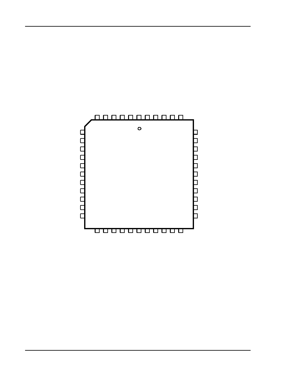
Figure 2: 44-Pin PLCC
XO
XI/FIN
DVDD
RESET*
D[1]
D[2]
D[3]
D[6]
D[4]
DVDD
D[5]
DGND
SC
SD
DGND]
D[7]
D[8]
D[9]
AVDD
VDD
ISET
GND
D0
]
V
XC
LK
*
XC
LK
VR
E
F
DVDD2
P-
O
U
T
H
DGND
DS/
B
C
O
AGND
D[1
0
]
D[1
1
]
GPI
O
[0]
DGND
GPI
O
[1]
DVDD
CSYNC
GND
CVBS
C
Y
7
8
9
10
13
12
11
39
38
37
36
35
14
15
16
17
34
33
32
31
30
29
6
5
4
3
2
1
44
43
42
41
40
18
19
20
21
24
23
22
25
26
27
28
CHRONTEL
CH7008
201-0000-027 Rev. 2.5, 5/2/2001
3
CHRONTEL
CH7008A
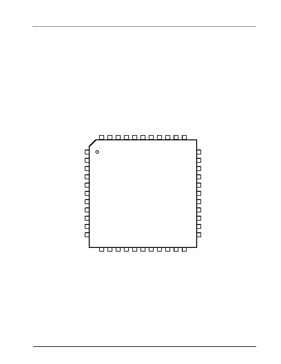
Figure 3: 44-Pin TQFP (1.4 mm)
XO
XI/FIN
DVDD
RESET*
D[1]
D[2]
D[3]
D[6]
D[4]
DVDD
D[5]
DGND
SC
SD
DGND]
D[7]
D[8]
D[9]
AVDD
VDD
ISET
GND
D0
]
V
XCLK*
XCLK
VREF
DVDD2
P-OU
T
H
DG
ND
DS/BCO
AG
ND
D[1
0
]
D[1
1
]
GP
I
O
[
0
]
DGND
GP
I
O
[
1
]
DVDD
CSYNC
GND
CVBS
C
Y
1
2
3
4
7
6
5
33
32
31
30
29
8
9
10
11
28
27
26
25
24
25
44
43
42
41
40
39
38
37
36
35
34
12
13
14
15
18
17
16
19
20
21
22
CHRONTEL
CH7008
CHRONTEL
CH7008A
4
201-0000-027 Rev. 2.5, 5/2/2001
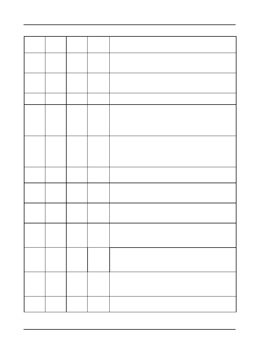
Table 1. Pin Descriptions
44-Pin
PLCC
44-Pin
TQFP
(1.4mm)
Type
Symbol
Description
1
39
In/Out
VREF
Reference Voltage Input
The VREF pin inputs a reference voltage of DVDD2/2. The signal is
derived externally through a resistor divider and decoupling capacitor,
and will be used as a reference level for data and sync inputs.
2
40
In
XCLK
External Clock Input
This input along with XCLK* will form a differential clock input. For
applications where a differential clock is not available, the XCLK* pin
should be connected to the VREF pin.
3
41
In
XCLK*
External Clock Input*
See XCLK description
4
42
In/Out
H
Horizontal Sync Input/Output
When the SYO bit is low, this pin accepts a horizontal sync input. The
level is 0 to DVDD2, with VREF as the threshold level.
When the SYO bit is high, the device will output a horizontal sync pulse.
The output is driven from the DVDD supply.
5
43
In/Out
V
Vertical Sync Input/Output
When the SYO bit is low, this pin accepts a vertical sync input. The level
is 0 to DVDD2 with VREF as the threshold level.
When the SYO bit is high, the device will output a vertical sync pulse.
The output is driven from the DVDD supply.
6-10,12-
13,15-19
44,1-4,6-
7,9-13
In
D[0]-D[11]
Data [0] through Data [11] Inputs
These pins accept 12 data inputs from the graphics controller. The level
is 0 to DVDD2, with VREF as the threshold level.
20-21
14-15
In/Out
GPIO[0]
GPIO[1]
General Purpose Input/Output [0-1] and Internal pull-up
These pins provide general purpose I/O's controlled via the IIC bus,
registers 1Bh and 1Ch, bits 7 and 6. The internal pull-up is to the DVDD
supply.
23
17
Out
CSYNC
Composite Sync Output
A 75
termination resistor with short traces should be attached
between CSYNC and ground for optimum performance. In SCART
mode, this pin outputs the composite sync signal.
26
20
Out
CVBS/B
Composite Video Output/Blue Output
A 75
termination resistor with short traces should be attached
between CVBS and ground for optimum performance. In normal
operating modes other than SCART, this pin outputs the composite
video signal. In SCART mode, this pin outputs the blue signal.
27
21
Out
C/G
Chroma Output/Green Output
A 75
termination resistor with short traces should be attached
between C and ground for optimum performance.
In normal operating
modes other than SCART, this pin outputs the chroma video signal. In
SCART mode, this pin outputs the green signal.
28
22
Out
Y/R
Luma Output / Red Output
A 75
termination resistor with short traces should be attached
between Y and ground for optimum performance.
In normal operating
modes other than SCART, this pin outputs the luma video signal. In
SCART mode, this pin outputs the red signal.
30
24
In
ISET
Current Set Resistor Input
This pin sets the DAC current. A 360 ohm resistor should be
connected between this pin and GND using short and wide traces.
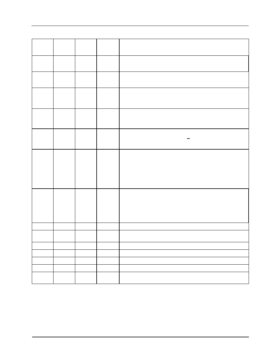
201-0000-027 Rev. 2.5, 5/2/2001
5
CHRONTEL
CH7008A
44-Pin
PLCC
44-Pin
TQFP
(1.4mm)
Type
Symbol
Description
32
26
In/Out
SD
Serial Data Input/Output
This pin functions as the serial data pin of the serial port, and uses the
DVDD supply.
33
27
In
SC
Serial Clock Input
This pin functions as the serial clock pin of the serial port, and uses
the DVDD supply.
35
29
In RESET*
Reset* Input
When this pin is low, the CH7008 is held in the power-on reset
condition. When this pin is high, the device operates normally and reset
is controlled through the serial port register.
38 32
In
XI/FIN
Crystal Input/External Reference Input
A parallel resonance 14.31818MHz crystal should be attached
between this pin and XO. However, an external CMOS clock can be
attached to XI/FIN.
39
33
Out
XO
Crystal Output
A parallel resonance 14.31818MHz +20ppm crystal should be
attached between this pin and XI/FIN. However, if an external CMOS
clock is attached to XI/FIN, XO should not be connected.
41
35
In/Out
DS/BCO
Data start (input)/Buffered Clock (output)
In normal operating modes, when configured as an input, the rising
edge of this signal identifies the first active pixel of data for each
active line. The level is 0 to DVDD2, with VREF as the threshold level.
When configured as an output this pin provides a buffered clock
output, driven by the DVDD supply. The output clock can be selected
using the BCO register (17th) (see Registers and Programing).
43
37
Out
P-OUT
Pixel Clock Output
This pin provides a pixel clock signal to the VGA controller (adjustable as
1X, 2X and 3X) and is driven from the DVDD2 supply. This clock will only
be provided in master clock modes, and will be tri-stated otherwise, (see
the section on Digital Video Interface and Registers and Programming
for more details). The capacitive loading on this pin should be kept to a
minimum.
11,22,36
5,16,30
Power
DVDD
Digital Supply Voltage
14,24,34,
42
8,18,28,3
6
Power
DGND
Digital Ground
25,29
19,23
Power
GND
DAC
31
25
Power
VDD
DAC Supply Voltage
37
31
Power AVDD
PLL Supply Voltage
40
34
Power
AGND
PLL Ground
44
38
Power
DVDD2
I/O SUPPLY VOLTAGE
Digital supply voltage for the P-OUT
Table 1. Pin Descriptions