 | –≠–ª–µ–∫—Ç—Ä–æ–Ω–Ω—ã–π –∫–æ–º–ø–æ–Ω–µ–Ω—Ç: CH7011A | –°–∫–∞—á–∞—Ç—å:  PDF PDF  ZIP ZIP |
CHRONTEL
CHRONTEL
CHRONTEL
CHRONTEL
CHRONTEL
Chrontel
201-0000-037 Rev 2.05, 6/6/2002
1
CH7011A
Chrontel CH7011 TV Output Device
1. F
EATURES
∑ TV output supporting graphics resolutions up to
1024x768 pixels
∑ Macrovision
TM
7.1.L1 copy protection support
∑ Programmable digital interface supports RGB and
YCrCb
∑ True scale rendering engine supports underscan in all
TV output resolutions
∑ Enhanced text sharpness and adaptive flicker
removal with up to 7 lines of filtering
∑ Support for all NTSC and PAL formats
∑ Provides CVBS, S-Video and SCART (RGB) outputs
∑ TV Programmable power management
∑ 10-bit video DAC outputs
∑ Fully programmable through serial port
∑ Complete Windows and DOS driver support
∑ Low voltage interface support to graphics device
∑ Offered in a 64-pin LQFP package
2. G
ENERAL
D
ESCRIPTION
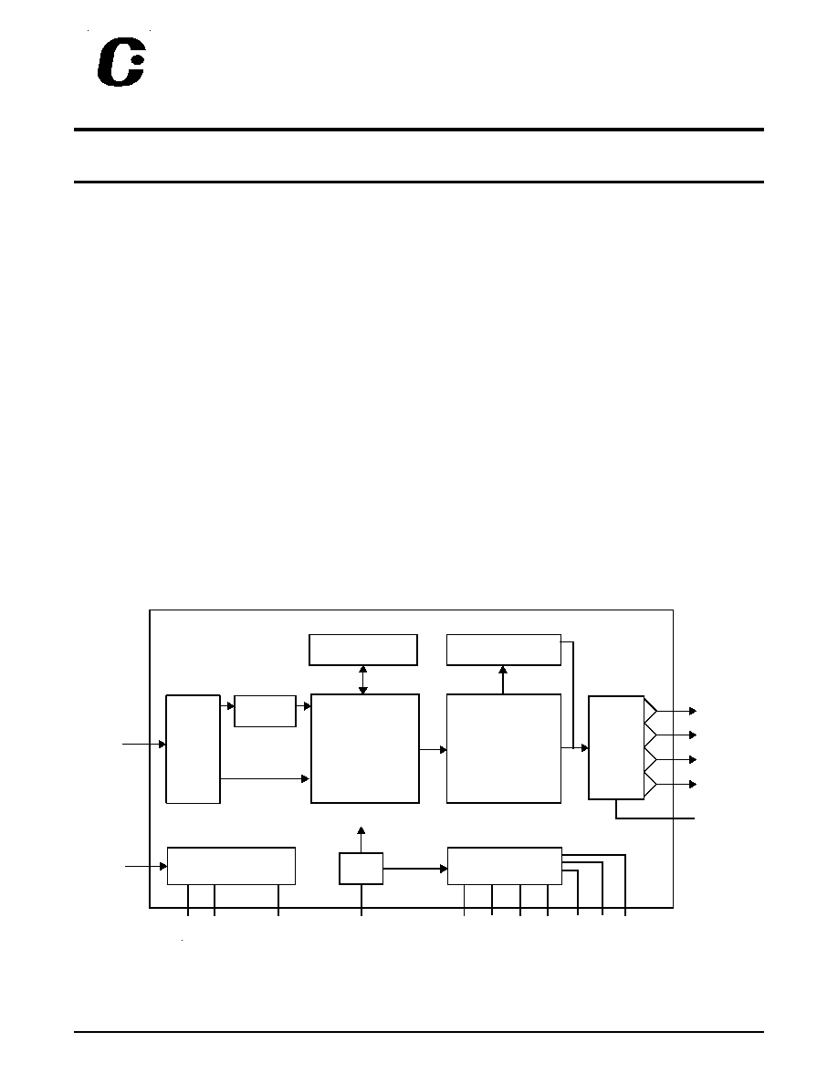
The CH7011 is a display controller device which
accepts a digital graphics input signal, and encodes and
transmits data to a TV output (analog composite, s-
video or RGB). The device accepts data over one 12-bit
wide variable voltage data port which supports five
different data formats including RGB and YCrCb.
The TV-Out processor will perform non-interlace to
interlace conversion with scaling and flicker filters, and
encode the data into any of the NTSC or PAL video
standards. The scaling and flicker filter is adaptive and
programmable to enable superior text display. Eight
graphics resolutions are supported up to 1024 by 768
with full vertical and horizontal underscan capability in
all modes. A high accuracy low jitter phase locked loop
is integrated to create outstanding video quality.
Support is provided for Macrovision
TM
and RGB bypass
mode which enables driving a VGA CRT with the input
data.
Figure 1: Functional Block Diagram
PLL
RGB-YUV
CONVERTER
SYSTEM CLOCK
YUV-RGB CONVERTER
DIGITAL
INPUT
INTERFACE
SERIAL PORT REGISTER &
CONTROL BLOCK
LINE
MEMORY
TRUE SCALE
SCALING &
DEFLICKERING
ENGINE
TIMING & SYNC
GENERATOR
NTSC/PAL
ENCODER
& FILTERS
D[11:0]
PIXEL DATA
XCLK/XCLK*
H
V
XI/FIN
XO
P-OUT
SPC
SPD
RESET*
BCO
CSYNC
GPIO[1:0]
Y/G (DAC1)
CVBS/B
(DAC0)
C/R (DAC2)
CVBS (DAC3)
Four
10-bit
DAC's
ISET

CHRONTEL
CH7011A
2
201-0000-037 Rev 2.05, 6/6/2002
3. P
IN
D
ESCRIPTIONS
3.1 Package Diagram
Figure 2: 64-Pin LQFP
DVDDV
C / H SYNC
Y / G
C / R
CVBS
ISET
VDD
GND
GND
AGND
XI / FIN
XO
AVDD
GPIO[1]
GPIO[0]
AS
DGND
AGND
AVDD
NC
NC
NC
NC
NC
NC
NC
NC
NC
NC
NC
NC
NC
NC
DGND
SPD
SPC
RESET*
NC
DVDD
VREF
DVDD
AGND
1
2
3
4
5
6
7
8
9
10
11
12
13
14
15
16
26
27
28
29
30
31
32
17
18
19
20
21
22
23
24
25
33
34
35
36
37
38
39
40
41
42
43
44
45
46
47
48
64
63
62
61
60
59
58
57
56
55
54
53
52
51
50
49
CVBS / B
Chrontel
XCLK
XCLK*
D[11]
D[10]
D[9]
D[8]
D[7]
D[6]
D[5]
D[4]
D[3]
D[2]
D[1]
D[0]
DGND
DVDD
H
V
NC
BCO
P-OUT
CH7011

201-0000-037 Rev 2.05, 6/6/2002
3
CHRONTEL
CH7011A
3.2 Pin Description
Table 1. Pin Description
64-Pin
LQFP
# Pins Type
Symbol
Description
3
1
In
VREF
Reference Voltage Input
The VREF pin inputs a reference voltage of DVDDV / 2. The
signal is derived externally through a resistor divider and
decoupling capacitor, and will be used as a reference level for
data, sync and clock inputs.
4
1
In/Out
H
Horizontal Sync Input / Output
When the SYO bit is low, this pin accepts a horizontal sync
input for use with the input data. The amplitude will be 0 to
DVDDV, and the VREF signal is used as the threshold level.
When the SYO bit is high, the device will output a horizontal
sync pulse, 64 pixels wide. The output is driven from the
DVDD. This output is only for use with the TV-Out function.
5
1
In/Out
V
Vertical Sync Input / Output
When the SYO bit is low, this pin accepts a vertical sync input
for use with the input data. The amplitude will be 0 to DVDDV,
and the VREF signal is used as the threshold level.
When the SYO bit is high, the device will output a vertical sync
pulse one line wide. The output is driven from the DVDD
supply. This output is only for use with the TV-Out function.
7
2
In/Out
GPIO[1]
General Purpose Input - Output[1]
(Open drain or weak pull-up (programmable))
This pin provides a general purpose I/O controlled via the serial
port bus.
8
2
In/Out
GPIO[0]
General Purpose Input - Output[0]
(Open drain or weak pull-up (programmable))
This pin provides a general purpose I/O controlled via the serial
port bus. This allows an external switch to be used to select
NTSC or PAL at power-up.
10
1
In
AS
Address Select (Internal pull-up)
This pin determines the serial port address of the device
(1,1,1,0,1,AS*,AS).
13
1
In
RESET*
Reset * Input (Internal pull-up)
When this pin is low, the device is held in the power-on reset
condition. When this pin is high, reset is controlled through the
serial port register.
14
1
In/Out
SPD
Serial Data Input / Output
This pin functions as the serial data pin of the serial port
interface, and uses the DVDD supply.
15
1
In
SPC
Serial Clock Input
This pin functions as the clock pin of the
serial port
interface,
and uses the DVDD supply.
35
1
In
ISET
Current Set Resistor Input
This pin sets the DAC current. A 140 ohm resistor should be
connected between this pin and GND (DAC ground) using
short and wide traces.

CHRONTEL
CH7011A
4
201-0000-037 Rev 2.05, 6/6/2002
64-Pin
LQFP
# Pins Type
Symbol
Description
36
1
Out
CVBS
Composite Video
This pin outputs a composite video signal capable of driving a
75 ohm doubly terminated load.
37
1
Out
Y/G
Luma / Green Output
This pin outputs a selectable video signal. The output is
designed to drive a 75 ohm doubly terminated load. The output
can be selected to be s-video luminance or green
.
38
1
Out
C/R
Chroma / Red Output
This pin outputs a selectable video signal. The output is
designed to drive a 75 ohm doubly terminated load. The output
can be selected to be s-video chrominance or red.
39
1
Out
CVBS/B
Composite Video / Blue Output
This pin outputs a selectable video signal. The output is
designed to drive a 75 ohm doubly terminated load. The output
can be selected to be composite video or blue.
42
1
In
XI / FIN
Crystal Input / External Reference Input
A parallel resonance 14.31818MHz crystal (+ 20 ppm) should
be attached between this pin and XO. However, an external
clock can drive the XI/FIN input.
43
1
In
XO
Crystal Output
A parallel resonance 14.31818MHz crystal (+ 20 ppm) should
be attached between this pin and XI / FIN. However, if an
external CMOS clock is attached to XI/FIN, XO should be left
open.
46
1
Out
P-OUT
Pixel Clock Output
When the CH7011 is operating as a VGA to TV encoder in
master clock mode, this pin provides a pixel clock signal to the
VGA controller which is used as a reference frequency. The
output is selectable between 1X or 2X of the pixel clock
frequency. The output driver is driven from the DVDDV
supply. This output has a programmable tri-state. The
capacitive loading on this pin should be kept to a minimum.
47
1
Out
BCO
Buffered Clock Output
This output pin provides a buffered clock output, driven by the
DVDD supply. The output clock can be selected using the BCO
register.
48
1
Out
C/H SYNC
Composite / Horizontal Sync Output
This pin can be selected to output a TV composite sync, TV
horizontal sync, or a buffered version of the VGA horizontal
sync. The output is driven from the DVDD supply.
50 ≠ 55,
58 ≠ 63
12
In
D[11] - D[0]
Data[11] through Data[0] Inputs
These pins accept the 12 data inputs from a digital video port
of a graphics controller. The levels are 0 to DVDDV, and the
VREF signal is used as the threshold level.
Table 1. Pin Description
201-0000-037 Rev 2.05, 6/6/2002
5
CHRONTEL
CH7011A
64-Pin
LQFP
# Pins Type
Symbol
Description
57, 56
2
In
XCLK,
XCLK*
External Clock Inputs
These inputs form a differential clock signal input to the
CH7011 for use with the H, V, DE and D[11:0] data. If
differential clocks are not available, the XCLK* input
should be connected to VREF.
The output clocks from this pad cell are able to have their
polarities reversed under the control of the MCP bit.
2, 9, 19, 21,
23, 24, 25,
27, 28, 30,
31
11
NC
No Connect
1, 12, 49
3
Power
DVDD
Digital Supply Voltage (3.3V)
6, 11, 64
3
Power
DGND
Digital Ground
45
1
Power
DVDDV
I/O Supply Voltage (3.3V to 1.1V)
23, 29
2
Power
NC
No Connect
20, 26, 32
3
Power
NC
No Connect
18, 44
2
Power
AVDD
PLL Supply Voltage (3.3V)
16, 17, 41
3
Power
AGND
PLL Ground
33
1
Power
VDD
DAC Supply Voltage (3.3V)
34, 40
2
Power
GND
DAC Ground
Table 1. Pin Description