 | –≠–ª–µ–∫—Ç—Ä–æ–Ω–Ω—ã–π –∫–æ–º–ø–æ–Ω–µ–Ω—Ç: CH7202 | –°–∫–∞—á–∞—Ç—å:  PDF PDF  ZIP ZIP |

201-0000-030 Rev 2.0, 6/2/99
1
CH7202
CHRONTEL
MPEG to TV Encoder with 8-bit Input
Features
∑ Outputs NTSC, PAL (B,D,G,H,I) and PAL-M (NTSC-
J or PAL-60 available as options)
∑ 8-bit YCrCb (4:2:2) input format
∑ Master or slave mode operation
∑ Triple 9-bit DAC for composite and S-video output
∑ 27 MHz DAC operating frequency eliminates
the need for 1/sinc(x) correction filter
∑ Low-jitter phase-locked loop circuitry operates using a
low-cost 14.31818 MHz crystal
∑ 40.5 or 33.9 MHz video decoder clock output
∑ 16.934 or 11.289 MHz audio decoder clock output
∑ 13.5 MHz and 27 MHz video pixel clock outputs
∑ Internal 4.6 MHz (m ax) luminance and 1.3 MHz
chrom inance filters
∑ Sub-carrier genlocked to HSYNC* and VSYNC*
∑ Sleep mode
∑ CMOS technology in 44-pin PLCC
∑ 5V single-supply operation
Description
The CH7202 video encoder integrates a dual PLL clock
generator and a digital NTSC/PAL video encoder. By
generating all essential clock signals for MPEG
playback, and converting digital video inputs to either
NTSC or PAL video signals, the CH7202 is an essential
component of any low-cost solution for video-CD
playback machines.
The CH7202 dual PLL clock synthesizer generates all
clocks and timing signals from a 14.31818 MHz
reference crystal (see application note 19 "Tuning
Clock Outputs" for selection and tuning of the 14.31818
MHz crystal). The CH7202 will accept HSYNC*,
VSYNC*, and 2XPCLK clock inputs during slave
mode operation. Timing signals from the PLLs can be
used to generate the horizontal and vertical sync signals
which enable operating the CH7202 in master mode.
The fully digital video encoder is pin-programmable to
generate either a 525-line NTSC or a 625-line PAL
compatible video signal. It also features a logic
selectable sleep mode which turns the encoder off while
leaving both PLL's running.
Figure 1: Functional Block Diagram
U
FILTER
V
FILTER
DAC
DAC
DAC
X
M
U
X
M
U
X
M
U
X
Y
FILTER
B LA NKIN G
COL O R-B URST
CO NT RO L
BL AN KING
H ,V SYNC
GEN ERATO R
X
S IN + COSINE
GENERATOR
ACLK
2XPCLK
Y
CVBS
C
YC[7:0],
IREF
RSET
AVDD
VDD
AGND
GND
XI XO/FIN
MOD0
MOD1
FS
L INE AR
INTE RP OLATO R
I NTE RFACE
PLL1
S TAT E
M ACHI NE
OSC
PLL2
PCLK
DCLK
HSYNC*
VSYNC*
8
CbSWAP
YCSWAP
M/S*
1/2
CHRONTEL
CH7202
2
201-0000-030 Rev 2.0, 6/2/99
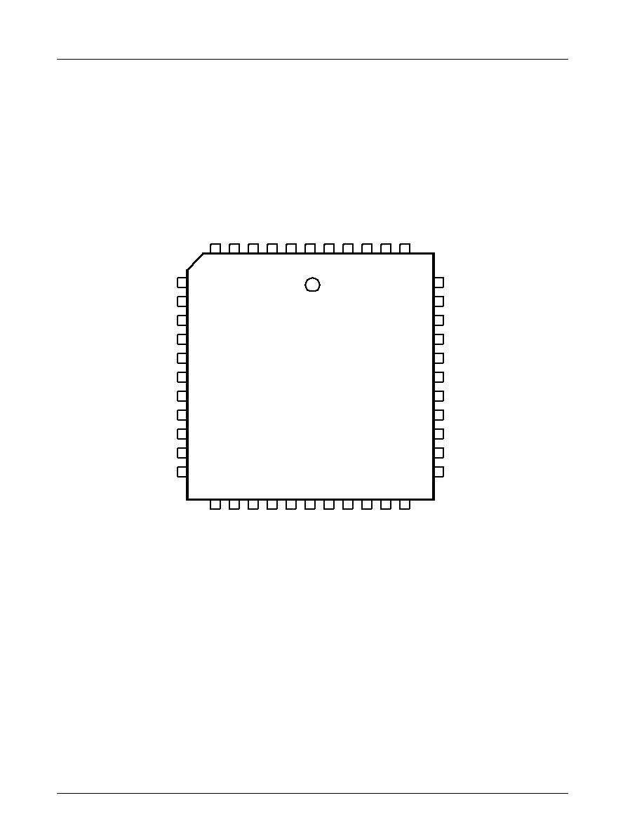
Figure 2: CH7202 Pinout Diagram
MOD0
VSYNC*
HSYNC*
GND
YC[1]
YCSWAP
FS
YC[6]
MOD1
CbSWAP
YC[7]
GND
Y
CVBS
YC[5]
YC[4]
YC[3]
YC[2]
VDD
C
AVDD
PCLK
AG
N
D
XI
VD
D
AC
LK
GN
D
2XPC
L
K
VD
D
X
O
/F
IN
DC
LK
GN
D
AV
DD
R
SET
YC
[0]
NC
NC
NC
NC
NC
NC
NC
M/
S
*
AG
N
D
7
8
9
10
13
12
11
39
38
37
36
35
14
15
16
17
34
33
32
31
30
29
6
5
4
3
2
1
44
43
42
41
40
18
19
20
21
24
23
22
25
26
27
28
CHRONTEL
CH7202

CHRONTEL
CH7202
201-0000-030 Rev 2.0, 6/2/99
3
Note:
1. Please refer to crystal manufacturer specifications for proper load capacitances. The optional variable tuning capacitor is
required only if the crystal oscillation frequency cannot be controlled to the required accuracy. The capacitance value for the tuning capac-
itor should be obtained from the crystal manufacturer. For further information, request a copy of Application Note AN-19, "Tuning Clock
Outputs."
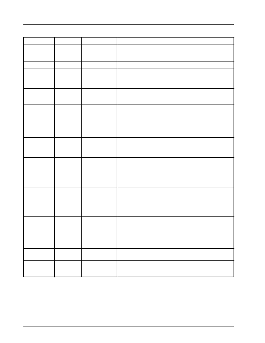
Table 1. Pin Descriptions
Pin
Type
Symbol
Description
1
Out
ACLK
Audio Decoder Clock Output
16.934 MHz or 11.289 MHz clock output (selectable by FS) for
MPEG audio decoder operation. The output swing is 5V.
2, 36, 42
Power
VDD
Digital Supply Voltage
These pins supply the 5V power to the digital section of the
CH7202.
3
In
XO/FIN
Crystal Output or External F
REF
Input
1
A parallel resonance 14.31818 MHz (±
50 ppm) crystal may be
attached between XO/FIN and XI. An external CMOS compatible
clock can be connected to XO/FIN as an alternative.
4
In
XI
Crystal Input
1
A parallel resonance 14.31818 MHz (±
50 ppm) crystal should be
attached between XI and XO/FIN. However, if an external CMOS
clock is attached to XO/FIN, XI should be connected to ground.
5, 27
Power
AGND
Analog ground
These pins provide the ground reference for the analog section of
the CH7202. These pins MUST be connected to the system
ground to prevent latchup.
6,29
Power
AVDD
Analog Supply Voltage
These pins supply the 5V power to the analog section of the
CH7202.
7
In
YCSWAP
Luma/Chroma Swap. Internally pulled-up.
YCSWAP=0 indicates a luminance sample is the first sample
following the leading edge of HSYNC*. YCSWAP=1 indicates a
chroma sample (Cb or CR depending on CbSWAP) is the first
sample following the leading edge of HSYNC*. See Figure 5 on
page 7.
8
In
FS
Frequency Select. Internally pulled-up
FS = 1 (default), then DCLK = 40.5 MHz, ACLK = 16.934 MHz
FS = 0, then DCLK = 33.9 MHz, ACLK = 11.289 MHz
9
In
MOD1
Mode bit 1 - Internally pulled-up
This input works in conjunction with the MOD0 input to select
NTSC, PAL, or Sleep mode functions. Refer to Table 3, "Video
Encoder Modes," on page 6 for details.
10
In
CbSWAP
Cb/Cr Swap. Internally pulled-up
When CbSWAP=0, the first chroma sample following the leading
edge of HSYNC* will be a Cb sample. When CbSWAP=1, the first
chroma sample following the leading edge of HSYNC* will be a Cr
sample. See Figure 5 on page 7
11 ≠ 18
In
YC[7:0]
Video Input
These pins accept the YCrCb data in CCIR656 (4:2:2) digital
video format. The sequence of the Y, Cb, Cr data is defined by
the YCSWAP and CbSWAP pins. For more details, please refer
to the timing diagram shown in Figure 5 on page 7.
Y has a nominal range of 16≠235.
Cb & Cr have a nominal range of 16≠240, with 128 equal to zero.
CHRONTEL
CH7202
4
201-0000-030 Rev 2.0, 6/2/99
Table 2. Pin Descriptions (continued)
Pin
Type
Symbol
Description
26
In
M/S*
Master/Slave* Internally pulled-up.
M/S*=1 then the CH7202 operates in master mode.
M/S*=0, then the CH7202 operates in slave mode.
19-25
In
NC
No Connect
28
In
RSET
Reference Resistor
A 360
resistor with short and wide traces should be attached
between RSET and ground. No other connections should be
made to this pin.
30
Out
C
Chrominance Output
A 75
termination resistor with short traces should be attached
between C and ground for optimum performance.
31
Out
CVBS
Composite Output
A 75
termination resistor with short traces should be attached
between CVBS and ground for optimum performance.
32
Out
Y
Luminance Output
A 75
termination resistor with short traces should be attached
between Y and ground for optimum performance.
33, 34, 40, 44
Power
GND
Digital Ground
These pins provide the ground reference for the digital section of
the CH7202. These pins MUST be connected to the system
ground through independent ground vias.
35
In/Out
HSYNC*
Horizontal Sync Input/Output
The horizontal sync output is generated by the CH7202 for master
mode operation. HSYNC* is an active low signal. In slave mode,
the horizontal sync becomes an input. For additional information,
please refer to the timing diagrams shown in Figures 6 and 7 on
page 8.
37
In/Out
VSYNC*
Vertical Sync Input/Output
The vertical sync output is generated by the CH7202 for master
mode operation. VSYNC* is an active low signal. In slave mode,
the vertical sync becomes an input. For additional information,
please refer to the timing diagrams shown in Figures 6 and 7 on
page 8.
38
In
MOD0
Mode bit 0 - internally pulled-up
This input works in conjunction with the MOD1 input to select
NTSC, PAL, or Sleep Mode functions. Refer to Table 3, "Video
Encoder Modes," on page 6 for details.
39
Out
PCLK
Video Pixel Clock Output
13.5 MHz clock output.
41
Out
DCLK
MPEG Decoder Clock Output
40.5 MHz or 33.9 MHz clock output (selectable by FS).
43
In/Out
2XPCLK
Double Pixel Clock Input/Output
27 MHz clock output. In slave mode, this pin becomes a 27 MHz
clock input.
CHRONTEL
CH7202
201-0000-030 Rev 2.0, 6/2/99
5
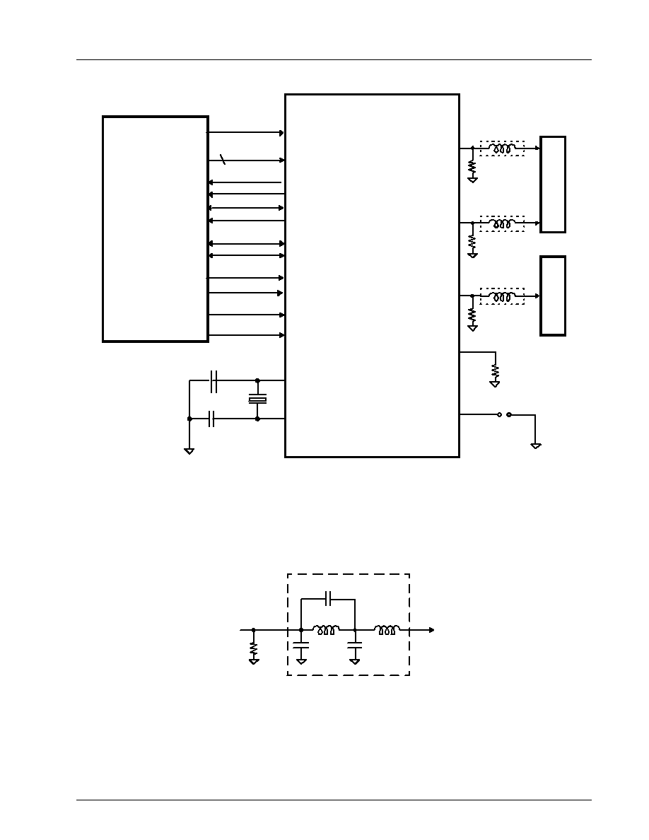
Figure 3: CH7202 Interface Diagram
Note:
1.
Please refer to the Optional Output Filter diagram below.
Note:
2. The proper value of these capacitors depends on the crystal manufacturer's specifications. Please refer to AN06 for the
details of the calculation.
Figure 4: Optional Output Filter
14.318
MHz
XI
XO/FIN
3
75
Y
C
CVBS
S-
Vi
d
e
o
Co
n
n
e
c
t
o
r
CH7202
Ferrite Bead
1
32
75
Ferrite Bead
1
30
75
Ferrite Bead
1
31
360
RSET
28
C
o
m
pos
i
t
e
C
onne
c
t
or
4
MPEG Decoder
and
System Controller
8
YC[7:0]
ACLK
DCLK
2XPCLK
VSYNC*
HSYNC*
11 - 18
1
41
43
37
35
27 pF
2
27 pF
2
FS
JUMPER
YCSWAP
CbSWAP
8
10
7
PCLK
39
MOD1
9
MOD0
38
M/S*
25
75
1.2
µ
H
47 pF
1.2
µ
H
270 pF
150 pF
Y, C, CVBS
OUTPUT