 | –≠–ª–µ–∫—Ç—Ä–æ–Ω–Ω—ã–π –∫–æ–º–ø–æ–Ω–µ–Ω—Ç: CH7303 | –°–∫–∞—á–∞—Ç—å:  PDF PDF  ZIP ZIP |
CH7303
Brief Datasheet
209-0000-031
Rev. 1.1, 4/24/2003
1
Chrontel
CH7303 HDTV / DVI Encoder
Features
1.0
General Description
∑ Digital Visual Interface (DVI) Transmitter up to 165M
pixels/second
∑ DVI low jitter PLL with Emission Reduction
∑ DVI hot plug detection
∑ Analog YPrPb outputs for HDTV
∑ HDTV support for 525p, 625p, 720p, 1080i and
1080p
∑ Macrovision
TM
copy protection support for 525p
and 625p
∑ Programmable digital input 16-bit D[15:0] interface
supporting RGB (15, 16, 24 or 30 bit) and YCrCb
input data formats
∑ Can output either RGB or YPrPb
∑ TV / Monitor connection detection
∑ Programmable power management
∑ Three 10-bit video DAC outputs
∑ Fully programmable through serial port
∑ Complete Windows and DOS driver support
∑ Low voltage interface support to graphics device
∑ Offered in a 64-pin LQFP package
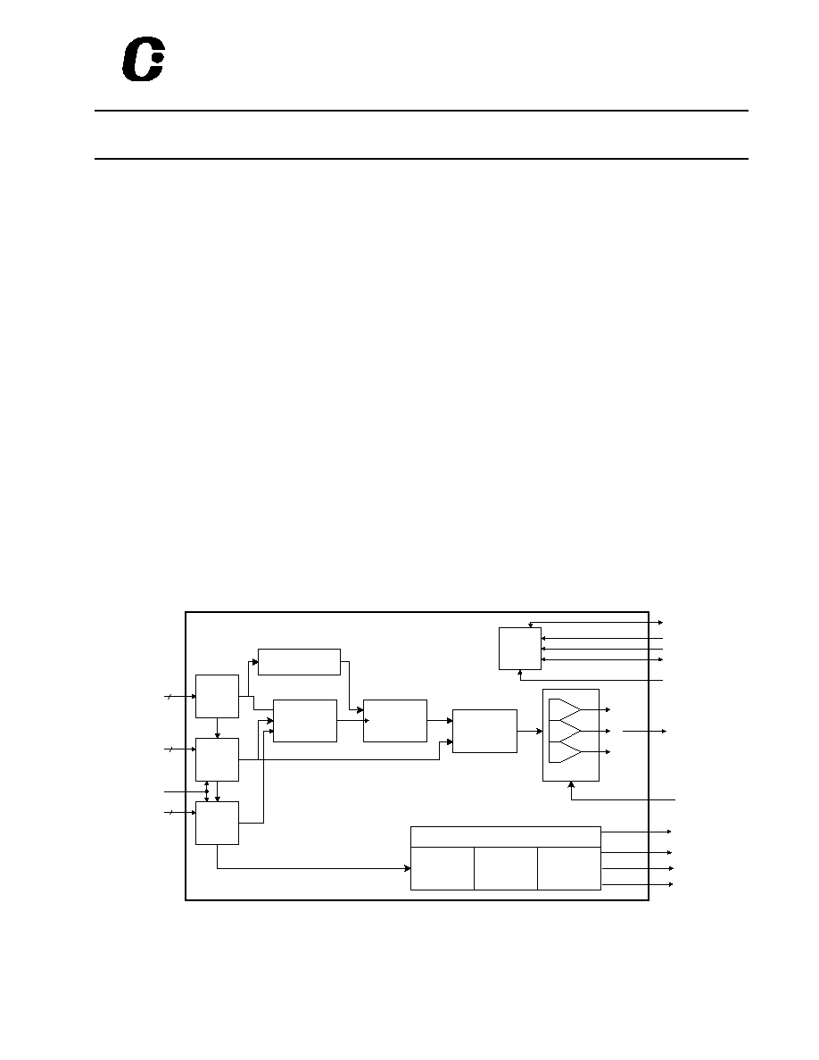
The CH7303 is a Display Controller device which accepts
a digital graphics input signal, and encodes and transmits data
through a DVI link (DFP can also be supported), VGA port
(analog RGB) or an HDTV port (YPrPb). The device accepts
data over one 16-bit wide variable voltage data port which
supports different data formats including RGB and YCrCb.
The device is able to generate and insert synchronization
signals for analog HDTV interface standards. Color space
conversion from RGB and YCrCb to YPrPb is supported
The DVI processor includes a low jitter PLL for
generation of the high frequency serialized clock, and all
circuitry required to encode, serialize and transmit data.
The CH7303 is able to drive a DFP display at a pixel rate
of up to 165MHz, supporting UXGA resolution displays.
No scaling of input data is performed on the data output
to the DVI device.
In addition to DVI encoder and HDTV modes, bypass modes
are included which output VGA style analog RGB for use as
a CRT DAC supporting graphics standards up to UXGA.
Color space conversion from YCrCb to RGB is supported
in both DVI and VGA bypass modes.
XCLK,XCLK*
Serial
Port
Control
D[15:0]
H,V
Data
Latch,
Demux
2
15
H,V
Latch
Clock
Driver
SPC
SPD
VREF
GPIO[1:0]
RESET*
ISET
Timing
Color Space
Conversion
Sync Decode
HDTV Sync
Generation
MUX
YPbPr
2
Three
10-bit DAC's
DAC 2
DAC 1
DAC 0
DAC[2:0]
DVI PLL
DVI Encode
DVI
Serialize
DVI Driver
/
2
/
2
/
2
/
2
TLC, TLC*
TDC0, TDC0*
TDC1, TDC1*
TDC2, TDC2*
RGB
/
30
/
3
AS
Figure 1: Functional Block Diagram

CHRONTEL
CH7303
2 209-0000-031
Rev. 1.1, 4/24/2003
2.0
Pin-Out
2.1
Package Diagram
VDDV
HSYNC
G/Y
R/Pr
TEST
ISET
DAC_VDD
DAC_GND
DAC_GND
D[15]
D[14]
D[13]
N/C
GPIO[1]/HPINT
GPIO[0]
AS
DGND
AGND
AVDD
VSWING
TDC2
*
TDC2
TLC
TLC*
TDC0
TDC0
*
TDC1
TDC1
*
TVDD
TVDD
TG
ND
TG
ND
TG
ND
DGND
SPD
SPC
RESET*
HPDET
DVDD
VREF
DVDD
N/C
B/Pb
Chrontel
XCLK
XCLK*
D
[
11]
D
[
10]
D[9
]
D[8
]
D[7
]
D[6
]
D[5
]
D[4
]
D[3
]
D[2
]
D[1
]
D[0
]
DGND
DVDD
H
V
DE
VSYNC
D[12]
CH7303
1
2
3
4
5
6
7
8
9
10
11
12
13
14
15
16
64
63
62
61
60
59
58
57
56
55
54
53
52
51
50
49
33
34
35
36
37
38
39
40
41
42
43
44
45
46
47
48
26
27
28
29
30
31
32
17
18
19
20
21
22
23
24
25
Figure 2: 64-Pin LQFP Package ≠ CH7303
CHRONTEL
CH7303
209-0000-031
Rev. 1.1, 4/24/2003
3
2.2
Pin Description
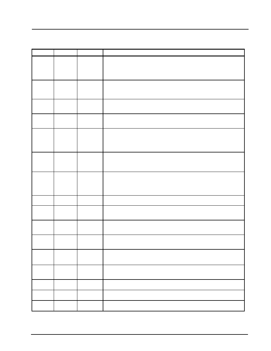
Table 1: Pin Description
Pin #
Type
Symbol
Description
2 In DE Data Enable
This pin accepts a data enable signal which is high when active video data is input to
the device, and low all other times. The levels are 0 to VDDV, and the VREF signal is
used as the threshold level. This input is used by the DVI. The TV-Out function uses H
and V sync as reference to active video.
3 In VREF
Reference Voltage Input
The VREF pin inputs a reference voltage of VDDV / 2. The signal is derived
externally through a resistor divider and decoupling capacitor, and will be used as a
reference level for data, sync, data enable and clock inputs.
4 In H Horizontal Sync Input
This pin accepts a horizontal sync input for use with the input data. The amplitude will
be 0 to VDDV and the VREF signal is used as the threshold level.
5 In V Vertical Sync Input
This pin accepts a vertical sync input for use with the input data. The amplitude will be
0 to VDDV and the VREF signal is used as the threshold level.
7 In/Out
GPIO[1]
/
HPINT
General Purpose Input - Output[1] / Hot Plug Interrupt
When the GPIO[1] pin is configured as an output, this pin can be used to output the
DVI detect signal (pulls low when a termination change has been detected on the
HPDET input). This is an open drain output. The output is released through serial
port control.
8 In/Out
GPIO[0]
General Purpose Input - Output[0]
(Weak internal pull-up)
This pin provides a general purpose I/O controlled via the serial port. The internal pull-
up will be to the DVDD supply.
9 In HPDET
Hot Plug Detect (internal pull-down)
This input pin determines whether the DVI is connected to a DVI monitor. When
terminated, the monitor is required to apply a voltage greater than 2.4 volts. Changes
on the status of this pin will be relayed to the graphics controller via GPIO[1]/HPINT
pin pulling low.
10 In AS Address Select (Internal pull-up)
This pin determines the serial port address of the device (1,1,1,0,1,AS*,AS).
13 In RESET*
Reset* Input (Internal pull-up)
When this pin is low, the device is held in the power-on reset condition. When this pin
is high, reset is controlled through the serial port register.
14 In/Out
SPD Serial Port Data Input / Output
This pin functions as the bi-directional data pin of the serial port and operates with
inputs from 0 to VDDV. Outputs are driven from 0 to VDDV.
15 In SPC Serial Port Clock Input
This pin functions as the clock input of the serial port and operates with inputs from 0
to VDDV.
19 In VSWING
DVI Swing Control
This pin sets the swing level of the DVI outputs. A 2.4K ohm resistor should be
connected between this pin and TGND using short and wide traces.
22, 21
Out
TLC,
TLC*
DVI Clock Outputs
These pins provide the differential clock output for the DVI interface corresponding to
data on the TDC[2:0] outputs.
25, 24
Out
TDC0,
TDC0*
DVI Data Channel 0 Outputs
These pins provide the DVI differential outputs for data channel 0 (blue).
28, 27
Out
TDC1,
TDC1*
DVI Data Channel 1 Outputs
These pins provide the DVI differential outputs for data channel 1 (green).
30, 31
Out
TDC2*,
TDC2
DVI Data Channel 2 Outputs
These pins provide the DVI differential outputs for data channel 2 (red).
CHRONTEL
CH7303
4 209-0000-031
Rev. 1.1, 4/24/2003
Table 1: Pin Description (contd.)
Pin #
Type
Symbol
Description
35 In ISET Current Set Resistor Input
This pin sets the DAC current. A 140 ohm resistor should be connected between this
pin and DAC ground (pins 34 and 40) using short and wide traces.
36 In TEST TEST Input
This pin is used for factory test and should be tied to GND or left N/C.
37 Out Y/G
(DAC1)
Luma / Green Output
This pin outputs a selectable video signal. The output is designed to drive a 75ohm
doubly terminated load. The output can be selected to be the luminance component of
YPrPb or Green component of RGB.
38 Out R/Pr
(DAC2)
Red / Pr Output
This pin outputs a selectable video signal. The output is designed to drive a 75ohm
doubly terminated load. The output can be selected to be the Pr component of YPrPb
or Red component of RGB.
39 Out B/Pb
(DAC0)
Blue / Pb Output
This pin outputs a selectable video signal. The output is designed to drive a 75ohm
doubly terminated load. The output can be selected to be the Pb component of YPrPb
or Blue component of RGB.
47 Out VSYNC
Vertical Sync Output
A buffered version of VGA vertical sync can be acquired from this pin. (Refer to
Register 21h
, bit [3] of DC register)
48 Out HSYNC
Horizontal Sync Output
A buffered version of VGA horizontal sync can be acquired from this pin. (Refer to
Register 21h
, bit [3] of DC register)
41 - 43,
46, 50 ≠
55,
58 ≠63
In/Out
D[15] - D[0] Data[15] through Data[0] Inputs
These pins accept the 16 data inputs from a digital video port of a graphics controller.
The levels are 0 to VDDV, and the VREF signal is used as the threshold level.
57, 56
In
XCLK,
XCLK*
External Clock Inputs
These inputs form a differential clock signal input to the CH7303 for use with the H,
V, DE and D[15:0] data. If differential clocks are not available, the XCLK* input pin
should be connected to VREF.
The clock polarity used for latching data can be selected using the MCP control bit.
1, 12, 49
Power
DVDD
Digital Supply Voltage (3.3V)
6, 11, 64
Power
DGND
Digital Ground
45 Power
VDDV
I/O Supply Voltage (1.1V to 3.3V)
23, 29
Power
TVDD
DVI Transmitter Supply Voltage (3.3V)
20, 26, 32 Power
TGND
DVI Transmitter Ground
18 Power
AVDD
PLL Supply Voltage (3.3V)
17 Power
AGND
PLL Ground
33 Power
DAC_VDD
DAC Supply Voltage (3.3V)
34, 40
Power
DAC_GND DAC Ground

CHRONTEL
CH7303
209-0000-031
Rev. 1.1, 4/24/2003
5
3.0
Package Dimensions
A
C
D
I
H
J
G
E
B
A
F
.004 "
LEAD
CO-PLANARITY
1
B
Table of Dimensions
No. of Leads
SYMBOL
64 (10 X 10 mm)
A
B
C
D
E
F
G
H
I
J
MIN 0.17
1.35
0.05
0.45
0.09
0∞
Milli-
meters
MAX
12 10 0.50
0.27 1.45 0.15
1.00
0.75 0.20 7∞
Figure 3: 64 Pin LQFP Package