
Preliminary Product Information
This document contains information for a new product.
Cirrus Logic reserves the right to modify this product without notice.
1
Copyright
© Cirrus Logic, Inc. 2002
(All Rights Reserved)
http://www.cirrus.com
CS4340A
24-Bit, 192 kHz Stereo DAC for Audio
Features
101 dB Dynamic Range
-91 dB THD+N
+3.3 V or +5 V Power Supply
50 mW with 3.3 V supply
Low Clock Jitter Sensitivity
Filtered Line Level Outputs
On-Chip Digital De-emphasis for 44.1kHz
Popguard
Æ
Technology for Control of Clicks
and Pops
Up to 200 kHz Sample Rates
Automatic Mode Detection for Sample Rates
between 4 and 200 kHz
Pin Compatible with the CS4340
Description
The CS4340A is a complete stereo digital-to-analog sys-
tem including digital interpolation, fourth-order delta-
sigma digital-to-analog conversion, digital de-emphasis
and switched capacitor analog filtering. The advantages
of this architecture include: ideal differential linearity, no
distortion mechanisms due to resistor matching errors,
no linearity drift over time and temperature, and a high
tolerance to clock jitter.
The CS4340A accepts data at all standard audio sample
rates up to 192 kHz, consumes very little power, oper-
ates over a wide power supply range and is pin
compatible with the CS4340, as described in section 3.1.
These features are ideal for DVD audio players.
ORDERING INFORMATION
CS4340A-KS
16-pin SOIC, -10 to 70 ∞C
CDB4340A
Evaluation Board
DAC
Analog Filter
Serial
Audio
Interface
Interpolation
Filter
Analog Filter
M UTEC
AO UT L
AO UTR
RST
LRCK
SDIN
M CLK
External
Mute Control
SCLK
DAC
Interpolation
Filter
De-emphasis
DEM
DIF0
DIF1
OCT `02
DS590PP2

CS4340A
2
DS590PP2
TABLE OF CONTENTS
1. PIN DESCRIPTION ......................................................................................... 4
2. TYPICAL CONNECTION DIAGRAM .............................................................. 5
3. APPLICATIONS .............................................................................................. 6
3.1 Upgrading from the CS4340 to the CS4340A ...................................... 6
3.2 Sample Rate Range/Operational Mode Detect ................................... 6
3.3 System Clocking .................................................................................. 6
3.4 Digital Interface Format ....................................................................... 7
3.5 De-Emphasis ....................................................................................... 8
3.6 Power-up Sequence ............................................................................ 9
3.7 Popguard
Æ
Transient Control .............................................................. 9
3.7.1 Power-up .................................................................................... 9
3.7.2 Power-down ............................................................................... 9
3.7.3 Discharge Time .......................................................................... 9
3.8 Mute Control ...................................................................................... 10
3.9 Grounding and Power Supply Arrangements .................................... 10
4. CHARACTERISTICS AND SPECIFICATIONS ............................................ 11
ANALOG CHARACTERISTICS (CS4340A-KS) ........................................ 11
COMBINED INTERPOLATION
& ON-CHIP ANALOG FILTER RESPONSE.............................................. 13
SWITCHING SPECIFICATIONS - SERIAL AUDIO INTERFACE ............. 16
DC ELECTRICAL CHARACTERISTICS ................................................... 17
DIGITAL INTERFACE SPECIFICATIONS ................................................ 17
DIGITAL INPUT CHARACTERISTICS ...................................................... 17
THERMAL CHARACTERISTICS AND SPECIFICATIONS ....................... 17
RECOMMENDED OPERATING SPECIFICATION ................................. 18
ABSOLUTE MAXIMUM RATINGS ............................................................ 18
5. PARAMETER DEFINITIONS ........................................................................ 19
6. REFERENCES .............................................................................................. 19
7. PACKAGE DIMENSIONS ............................................................................. 20
Contacting Cirrus Logic Support
For all product questions and inquiries contact a Cirrus Logic Sales Representative.
To find one nearest you go to
http://www.cirrus.com/corporate/contacts/sales.cfm
IMPORTANT NOTICE
"Preliminary" product information describes products that are in production, but for which full characterization data is not yet available. "Advance" product infor-
mation describes products that are in development and subject to development changes. Cirrus Logic, Inc. and its subsidiaries ("Cirrus") believe that the infor-
mation contained in this document is accurate and reliable. However, the information is subject to change without notice and is provided "AS IS" without warranty
of any kind (express or implied). Customers are advised to obtain the latest version of relevant information to verify, before placing orders, that information being
relied on is current and complete. All products are sold subject to the terms and conditions of sale supplied at the time of order acknowledgment, including those
pertaining to warranty, patent infringement, and limitation of liability. No responsibility is assumed by Cirrus for the use of this information, including use of this
information as the basis for manufacture or sale of any items, or for infringement of patents or other rights of third parties. This document is the property of Cirrus
and by furnishing this information, Cirrus grants no license, express or implied under any patents, mask work rights, copyrights, trademarks, trade secrets or
other intellectual property rights. Cirrus owns the copyrights of the information contained herein and gives consent for copies to be made of the information only
for use within your organization with respect to Cirrus integrated circuits or other parts of Cirrus. This consent does not extend to other copying such as copying
for general distribution, advertising or promotional purposes, or for creating any work for resale.
An export permit needs to be obtained from the competent authorities of the Japanese Government if any of the products or technologies described in this ma-
terial and controlled under the "Foreign Exchange and Foreign Trade Law" is to be exported or taken out of Japan. An export license and/or quota needs to be
obtained from the competent authorities of the Chinese Government if any of the products or technologies described in this material is subject to the PRC Foreign
Trade Law and is to be exported or taken out of the PRC.
CERTAIN APPLICATIONS USING SEMICONDUCTOR PRODUCTS MAY INVOLVE POTENTIAL RISKS OF DEATH, PERSONAL INJURY, OR SEVERE
PROPERTY OR ENVIRONMENTAL DAMAGE ("CRITICAL APPLICATIONS"). CIRRUS PRODUCTS ARE NOT DESIGNED, AUTHORIZED, OR WARRANT-
ED TO BE SUITABLE FOR USE IN LIFE-SUPPORT DEVICES OR SYSTEMS OR OTHER CRITICAL APPLICATIONS. INCLUSION OF CIRRUS PRODUCTS
IN SUCH APPLICATIONS IS UNDERSTOOD TO BE FULLY AT THE CUSTOMER'S RISK.
Cirrus Logic, Cirrus, and the Cirrus Logic logo designs are trademarks of Cirrus Logic, Inc. All other brand and product names in this document may be trade-
marks or service marks of their respective owners.

CS4340A
DS590PP2
3
LIST OF FIGURES
Figure 1. Typical Connection Diagram ............................................................................................ 5
Figure 2. CS4340A Format 0 - I
2
S up to 24-Bit Data ...................................................................... 7
Figure 3. CS4340A Format 1 - Left Justified up to 24-Bit Data....................................................... 8
Figure 4. CS4340A Format 2 - Right Justified, 24-Bit Data ............................................................ 8
Figure 5. CS4340A Format 3 - Right Justified, 16-Bit Data ............................................................ 8
Figure 6. De-Emphasis Curve......................................................................................................... 8
Figure 7. Output Test Load ........................................................................................................... 12
Figure 8. Maximum Loading.......................................................................................................... 12
Figure 9. Single-Speed Stopband Rejection ................................................................................. 14
Figure 10. Single-Speed Transition Band ..................................................................................... 14
Figure 11. Single-Speed Transition Band (Detail)......................................................................... 14
Figure 12. Single-Speed Passband Ripple ................................................................................... 14
Figure 13. Double-Speed Stopband Rejection.............................................................................. 14
Figure 14. Double-Speed Transition Band.................................................................................... 14
Figure 15. Double-Speed Transition Band (Detail) ....................................................................... 15
Figure 16. Double-Speed Passband Ripple.................................................................................. 15
Figure 17. Serial Input Timing ....................................................................................................... 16
LIST OF TABLES
Table 1. CS4340A Auto-Detect....................................................................................................... 6
Table 2. Single-Speed Mode Standard Frequencies ...................................................................... 7
Table 3. Double-Speed Mode Standard Frequencies..................................................................... 7
Table 4. Quad-Speed Mode Standard Frequencies ....................................................................... 7
Table 5. Digital Interface Format - DIF1 and DIF0 .......................................................................... 7
Table 6. De-Emphasis Control ........................................................................................................ 8
CS4340A
4
DS590PP2
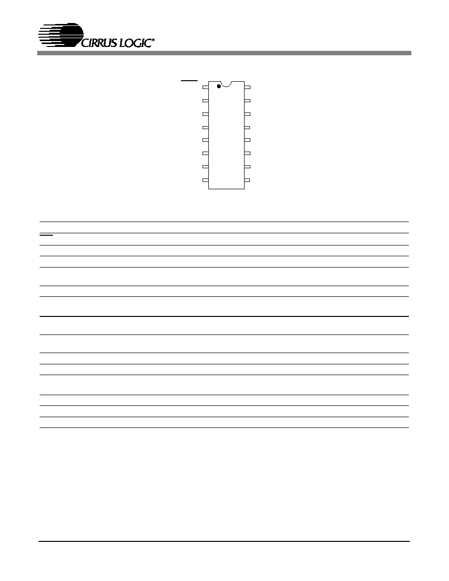
1. PIN DESCRIPTION
Pin Name
#
Pin Description
RST
1
Reset
(Input) - Powers down device.
SDIN
2
Serial Audio Data
(Input) - Input for two's complement serial audio data.
SCLK
3
Serial Clock
(Input) -Serial clock for the serial audio interface.
LRCK
4
Left Right Clock
(Input) - Determines which channel, Left or Right, is currently active on the
serial audio data line.
MCLK
5
Master Clock
(Input) - Clock source for the delta-sigma modulator and digital filters.
DIF1
DIF0
6
7
Digital Interface Format
(Input) - Defines the required relationship between the Left Right
Clock, Serial Clock and Serial Audio Data.
DEM
8
De-emphasis Control
(Input) - Selects the standard 15
µs/50µs digital de-emphasis filter
response for the 44.1 kHz sample rate.
FILT+
9
Positive Voltage Reference
(Output) - Positive voltage reference for the internal
sampling circuits.
VQ
10
Quiescent Voltage
(Output) - Filter connection for internal quiescent reference voltage.
REF_GND
11
Reference Ground
(Input) - Ground reference for the internal sampling circuits.
AOUTR
AOUTL
12
15
Analog Outputs
(Output) - The full scale analog output level is specified in the
Analog Characteristics
table.
AGND
13
Analog Ground
(Input)
VA
14
Power
(Input) - Positive power for the analog, digital and serial audio interface sections.
MUTEC
16
Mute Control
(Output) - Control signal for an optional mute circuit.
15
2
14
3
13
4
16
1
11
6
10
7
9
8
12
5
RST
MUTEC
SDIN
AOUTL
SCLK
VA
LRCK
AGND
MCLK
AOUTR
DIF1
REF_GND
DIF0
VQ
DEM
FILT+
