Advance Product Information
This document contains information for a new product.
Cirrus Logic reserves the right to modify this product without notice.
Copyright
�
Cirrus Logic, Inc. 2004
(All Rights Reserved)
http://www.cirrus.com
CS4385
114 dB, 192 kHz 8-Channel D/A Converter
Features
Advanced Multi-bit Delta Sigma Architecture
24-Bit Conversion
Automatic Detection of Sample Rates up to
192 kHz
114 dB Dynamic Range
-100 dB THD+N
Direct Stream Digital Mode
� Non-decimating volume control
� On-chip 50 kHz filter
� Matched PCM and DSD analog output levels
Compatible with Industry-standard Time
Division Multiplexed (TDM) Serial Interface
Selectable Digital Filters
Volume Control with 1/2-dB Step Size and
Soft Ramp
Low Clock Jitter Sensitivity
+5 V Analog Supply, +2.5 V Digital Supply
Separate 1.8 to 5 V Logic Supplies for the
Control & Serial Ports
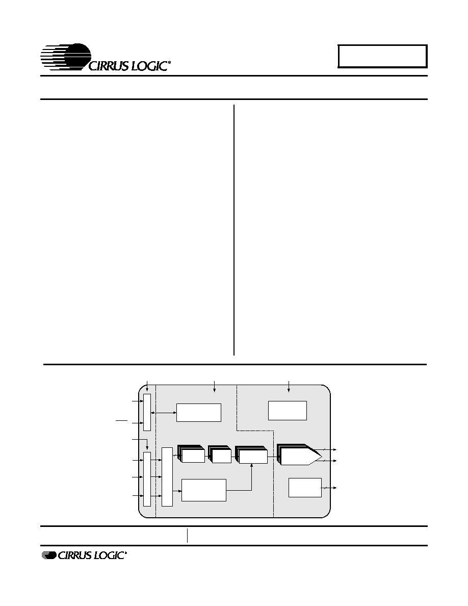
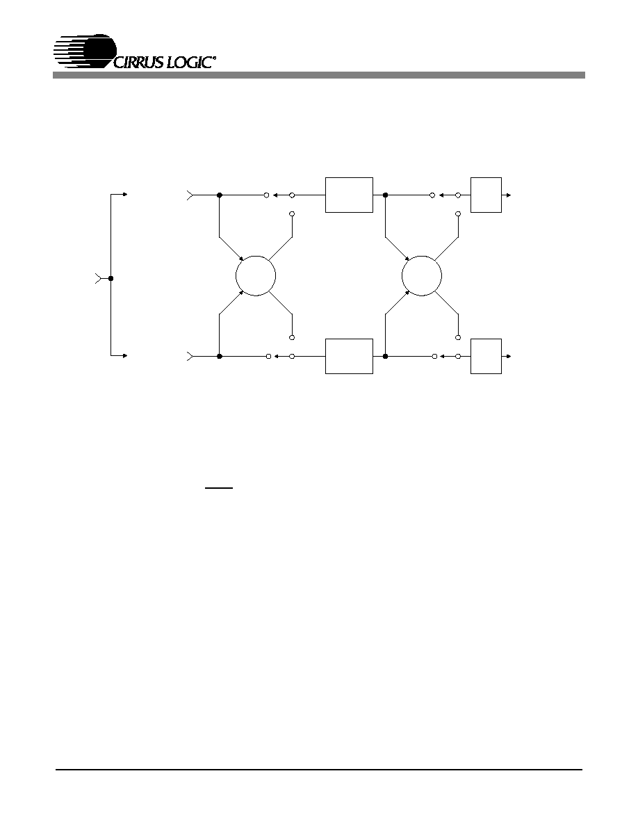
Description
The CS4385 is a complete 8-channel digital-to-analog
system. This D/A system includes digital de-emphasis,
half-dB step size volume control, ATAPI channel mixing,
selectable fast and slow digital interpolation filters fol-
lowed by an oversampled, multi-bit delta sigma
modulator which includes mismatch shaping technology
that eliminates distortion due to capacitor mismatch. Fol-
lowing this stage is a multi-element switched capacitor
stage and low-pass filter with differential analog outputs.
The CS4385 also has a proprietary DSD processor
which allows for volume control and 50 kHz on-chip filter-
ing without an intermediate decimation stage. It also
offers an optional path for direct DSD conversion by di-
rectly using the multi-element switched capacitor array.
The CS4385 accepts PCM data at sample rates from
4 kHz to 216 kHz, DSD audio data, and delivers excel-
lent sound quality. These features are ideal for multi-
channel audio systems including SACD players, A/V re-
ceivers, digital TV's, mixing consoles, effects
processors, sound cards and automotive audio systems.
ORDERING INFORMATION
CS4385-CQZ
-10 to 70
�
C 48-pin LQFP, Lead-Free
CS4385-DQZ
-40 to 85
�
C 48-pin LQFP, Lead-Free
CDB4385
Evaluation Board
I
C o ntrol Port Supp ly = 1.8 V to 5 V
Re giste r/H ardwa re
C onfigura tion
Inte rnal Voltage
Reference
Reset
S
e
ria
l
In
te
rfa
c
e
Le
ve
l
T
r
a
n
sl
a
t
or
Le
ve
l
T
r
a
n
sl
a
t
or
TD M Serial
A u dio In pu t
Digital S up p ly = 2.5 V
H ard w are Mod e o r
I
2
C /SP I S oftw are Mod e
C on tro l Data
A n alog S up p ly = 5 V
E ig ht C h an n els
o f Differen tial
O utpu ts
8
8
P C M S erial
A ud io In p ut
Volume
C ontrols
Digita l
F ilte rs
Switch-C a p
D AC and
A na log F ilte rs
Multi-bit
Modula tors
D SD A u dio
In pu t
DSD Processor
-Volume control
-50 kHz filter
E xterna l Mute
C ontrol
Mute S ig n als
2
8
Serial A u dio Po rt
Su p ply = 1.8 V to 5 V
OCT `04
DS671A1

CS4385
2
DS671A1
TABLE OF CONTENTS
1. PIN DESCRIPTION ................................................................................................................... 4
2. CHARACTERISTICS AND SPECIFICATIONS ........................................................................ 6
SPECIFIED OPERATING CONDITIONS ................................................................................. 6
ABSOLUTE MAXIMUM RATINGS ........................................................................................... 6
DAC ANALOG CHARACTERISTICS ....................................................................................... 7
POWER AND THERMAL CHARACTERISTICS....................................................................... 8
COMBINED INTERPOLATION & ON-CHIP ANALOG FILTER RESPONSE........................... 9
DSD COMBINED DIGITAL AND ON-CHIP ANALOG FILTER RESPONSE.......................... 10
DIGITAL CHARACTERISTICS ............................................................................................... 11
SWITCHING CHARACTERISTICS - PCM ............................................................................. 12
SWITCHING CHARACTERISTICS - DSD.............................................................................. 13
SWITCHING CHARACTERISTICS - CONTROL PORT - I
2
C FORMAT ................................ 14
SWITCHING CHARACTERISTICS - CONTROL PORT - SPI FORMAT ............................... 15
3. APPLICATIONS ...................................................................................................................... 18
3.1 Master Clock .................................................................................................................... 18
3.2 Mode Select ..................................................................................................................... 19
3.3 Digital Interface Formats ................................................................................................. 20
3.3.1 OLM #1 ............................................................................................................... 21
3.3.2 OLM #2 ............................................................................................................... 22
3.3.3 OLM #3 ............................................................................................................... 22
3.3.4 OLM #4 ............................................................................................................... 22
3.3.5 TDM .................................................................................................................... 23
3.4 Oversampling Modes ....................................................................................................... 23
3.5 Interpolation Filter ............................................................................................................ 23
3.6 De-Emphasis ................................................................................................................... 24
3.7 ATAPI Specification ......................................................................................................... 25
3.8 Direct Stream Digital (DSD) Mode ................................................................................... 25
3.9 Grounding and Power Supply Arrangements .................................................................. 26
3.9.1 Capacitor Placement ........................................................................................... 27
3.10 Analog Output and Filtering ........................................................................................... 27
3.11 The MUTEC Outputs ..................................................................................................... 29
3.12 Recommended Power-up Sequence ............................................................................. 30
3.12.1 Hardware Mode ................................................................................................. 30
3.12.2 Software Mode .................................................................................................. 30
3.13 Control Port Interface ..................................................................................................... 31
3.13.1 MAP Auto Increment ......................................................................................... 31
3.13.2 I
2
C Mode ........................................................................................................... 31
3.13.3 SPI Mode .......................................................................................................... 33
3.14 Memory Address Pointer (MAP) .............................................................................. 34
4. REGISTER QUICK REFERENCE ......................................................................................... 35
5. REGISTER DESCRIPTION .................................................................................................... 37
6. PARAMETER DEFINITIONS .................................................................................................. 49
7. REFERENCES ........................................................................................................................ 49
8. PACKAGE DIMENSIONS ....................................................................................................... 50
9. APPENDIX ......................................................................................................................... 51

CS4385
DS671A1
3
LIST OF FIGURES
Figure 1. Serial Audio Interface Timing......................................................................................... 12
Figure 2. TDM Serial Audio Interface Timing ................................................................................ 12
Figure 3. Direct Stream Digital - Serial Audio Input Timing........................................................... 13
Figure 4. Direct Stream Digital - Serial Audio Input Timing for Phase Modulation mode.............. 13
Figure 5. Control Port Timing - I
2
C Format ................................................................................... 14
Figure 6. Control Port Timing - SPI Format................................................................................... 15
Figure 7. Typical Connection Diagram, Software Mode................................................................ 16
Figure 8. Typical Connection Diagram, Hardware ........................................................................ 17
Figure 9. Format 0 - Left Justified up to 24-bit Data...................................................................... 20
Figure 10. Format 1 - I
2
S up to 24-bit Data................................................................................... 20
Figure 11. Format 2 - Right Justified 16-bit Data .......................................................................... 20
Figure 12. Format 3 - Right Justified 24-bit Data .......................................................................... 20
Figure 13. Format 4 - Right Justified 20-bit Data .......................................................................... 21
Figure 14. Format 5 - Right Justified 18-bit Data .......................................................................... 21
Figure 15. Format 8 - One Line Mode 1........................................................................................ 21
Figure 16. Format 9 - One Line Mode 2........................................................................................ 22
Figure 17. Format 10 - One Line Mode 3...................................................................................... 22
Figure 18. Format 11 - One Line Mode 4...................................................................................... 22
Figure 19. Format 12 - TDM Mode................................................................................................ 23
Figure 20. De-Emphasis Curve..................................................................................................... 24
Figure 21. ATAPI Block Diagram (x = channel pair 1, 2, 3, or 4) .................................................. 25
Figure 22. DSD phase modulation mode diagram ........................................................................ 26
Figure 23. Full-Scale Output ......................................................................................................... 27
Figure 24. Recommended Output Filter........................................................................................ 28
Figure 25. Recommended Mute Circuitry ..................................................................................... 29
Figure 26. Control Port Timing, I
2
C Mode..................................................................................... 32
Figure 27. Control Port Timing, SPI mode .................................................................................... 33
Figure 28. Single Speed (fast) Stopband Rejection ...................................................................... 51
Figure 29. Single Speed (fast) Transition Band ............................................................................ 51
Figure 30. Single Speed (fast) Transition Band (detail) ................................................................ 51
Figure 31. Single Speed (fast) Passband Ripple .......................................................................... 51
Figure 32. Single Speed (slow) Stopband Rejection..................................................................... 51
Figure 33. Single Speed (slow) Transition Band........................................................................... 51
Figure 34. Single Speed (slow) Transition Band (detail)............................................................... 52
Figure 35. Single Speed (slow) Passband Ripple......................................................................... 52
Figure 36. Double Speed (fast) Stopband Rejection..................................................................... 52
Figure 37. Double Speed (fast) Transition Band........................................................................... 52
Figure 38. Double Speed (fast) Transition Band (detail)............................................................... 52
Figure 39. Double Speed (fast) Passband Ripple......................................................................... 52
Figure 40. Double Speed (slow) Stopband Rejection ................................................................... 53
Figure 41. Double Speed (slow) Transition Band ......................................................................... 53
Figure 42. Double Speed (slow) Transition Band (detail) ............................................................. 53
Figure 43. Double Speed (slow) Passband Ripple ....................................................................... 53
Figure 44. Quad Speed (fast) Stopband Rejection ....................................................................... 53
Figure 45. Quad Speed (fast) Transition Band ............................................................................. 53
Figure 46. Quad Speed (fast) Transition Band (detail) ................................................................. 54
Figure 47. Quad Speed (fast) Passband Ripple ........................................................................... 54
Figure 48. Quad Speed (slow) Stopband Rejection...................................................................... 54
Figure 49. Quad Speed (slow) Transition Band ............................................................................ 54
Figure 50. Quad Speed (slow) Transition Band (detail) ................................................................ 54
Figure 51. Quad Speed (slow) Passband Ripple .......................................................................... 54
CS4385
4
DS671A1
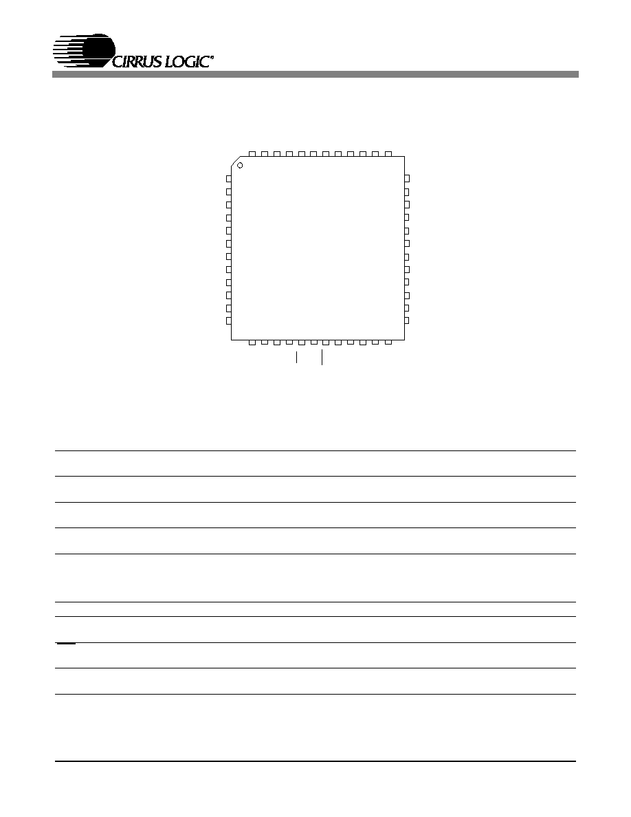
1.
PIN DESCRIPTION
Pin Name
#
Pin Description
VD
4
Digital Power (Input) - Positive power supply for the digital section. Refer to the Recommended Operat-
ing Conditions for appropriate voltages.
GND
5
31
Ground (Input) - Ground reference. Should be connected to analog ground.
MCLK
6
Master Clock (Input) - Clock source for the delta-sigma modulator and digital filters. Tables 1-3 illustrate
several standard audio sample rates and the required master clock frequency.
LRCK
7
Left Right Clock (Input) - Determines which channel, Left or Right, is currently active on the serial audio
data line. The frequency of the left/right clock must be at the audio sample rate, Fs.
SDIN1
SDIN2
SDIN3
SDIN4
8
11
13
14
Serial Audio Data Input (Input) - Input for two's complement serial audio data.
SCLK
9
Serial Clock (Input) - Serial clock for the serial audio interface.
VLC
18
Control Port Power (Input) - Determines the required signal level for the control port. Refer to the Rec-
ommended Operating Conditions for appropriate voltages.
RST
19
Reset (Input) - The device enters a low power mode and all internal registers are reset to their default
settings when low.
FILT+
20
Positive Voltage Reference (Output) - Positive reference voltage for the internal sampling circuits.
Requires the capacitive decoupling to analog ground, as shown in the Typical Connection Diagram.
SDI
N
3
GND
AOUTB2-
AOUTA3+
AOUTB3-
AOUTB2+
VA
AOUTA3-
AOUTB3+
AOUTA4-
AOUTA4+
6
2
4
8
10
1
3
5
7
9
11
12
13 14 15 16 17 18 19 20 21 22 23 24
31
35
33
29
27
36
34
32
30
28
26
25
48 47 46 45 44 43 42 41 40 39 38 37
MCLK
DSDB1
VD
SDIN1
M4(TST)
DSDA2
DSDA1
GND
SCLK
SDIN2
M3(TST)
LRCK
DSD_SCLK
DSDB3
DSDA3
DS
D
A
4
CS4385
DS
D
B
4
VL
S
SD
IN4
M2(
S
CL/
C
CLK)
M1(
S
DA/
C
DI
N)
VL
C
RST
FIL
T
+
VQ
MUT
E
C
2
34
AO
UTB4
-
AOUTB4
+
M0(
A
D0/C
S)
AOUTA2+
AOUTA2-
AOUTB1
+
AOUTB1
-
AOUTA1
-
AOUTA1
+
DS
DB
2
MU
T
E
C
1
CS4385
DS671A1
5
VQ
21
Quiescent Voltage (Output) - Filter connection for internal quiescent voltage. VQ must be capacitively
coupled to analog ground, as shown in the Typical Connection Diagram. The nominal voltage level is
specified in the Analog Characteristics and Specifications section. VQ presents an appreciable source
impedance and any current drawn from this pin will alter device performance. However, VQ can be
used to bias the analog circuitry assuming there is no AC signal component and the DC current is less
than the maximum specified in the Analog Characteristics and Specifications section.
MUTEC1
MUTEC234
41
22
Mute Control (Output) - The Mute Control pins go high during power-up initialization, reset, muting,
power-down or if the master clock to left/right clock frequency ratio is incorrect. These pins are intended
to be used as a control for external mute circuits to prevent the clicks and pops that can occur in any sin-
gle supply system. The use of external mute circuits are not mandatory but may be desired for designs
requiring the absolute minimum in extraneous clicks and pops.
AOUTA1 +,-
AOUTB1 +,-
AOUTA2 +,-
AOUTB2 +,-
AOUTA3 +,-
AOUTB3 +,-
AOUTA4 +,-
AOUTB4 +,-
39, 40
38, 37
35, 36
34, 33
29, 30
28, 27
25, 26
24, 23
Differential Analog Output (Output) - The full scale differential analog output level is specified in the
Analog Characteristics specification table.
VA
32
Analog Power (Input) - Positive power supply for the analog section. Refer to the Recommended Oper-
ating Conditions for appropriate voltages.
VLS
43
Serial Audio Interface Power (Input) - Determines the required signal level for the serial audio inter-
face. Refer to the Recommended Operating Conditions for appropriate voltages.
Software Mode Definitions
SCL/CCLK
15
Serial Control Port Clock (Input) - Serial clock for the serial control port. Requires an external pull-up
resistor to the logic interface voltage in I
2
C mode as shown in the Typical Connection Diagram.
SDA/CDIN
16
Serial Control Data (Input/Output) - SDA is a data I/O line in I
2
C mode and requires an external pull-up
resistor to the logic interface voltage, as shown in the Typical Connection Diagram. CDIN is the input
data line for the control port interface in SPI mode.
AD0/CS
17
Address Bit 0 (I
2
C) / Chip Select (SPI) (Input) - AD0 is a chip address pin in I
2
C mode; CS is the chip
select signal for SPI format.
TST
10
12
Test (Input) - These pins are not used in software mode and should not be left floating (connect to
ground).
Hardware Mode Definitions
M0
M1
M2
M3
M4
17
16
15
12
10
Mode Selection (Input) - Determines the operational mode of the device as detailed in Tables 4 and 5.
DSD Definitions
DSD_SCLK
42
DSD Serial Clock (Input) - Serial clock for the Direct Stream Digital audio interface.
DSDA1
DSDB1
DSDA2
DSDB2
DSDA3
DSDB3
DSDA4
DSDB4
3
2
1
48
47
46
45
44
Direct Stream Digital Input (Input) - Input for Direct Stream Digital serial audio data.
Pin Name
#
Pin Description
CS4385
6
DS671A1
2.
CHARACTERISTICS AND SPECIFICATIONS
(All Min/Max characteristics and specifications are guaranteed over the Specified Operating Conditions. Typical
performance characteristics and specifications are derived from measurements taken at nominal supply voltage
and T
A
= 25
�
C.)
SPECIFIED OPERATING CONDITIONS
(GND = 0 V; all voltages with respect to ground.)
ABSOLUTE MAXIMUM RATINGS
(GND = 0 V; all voltages with respect to ground.)
WARNING: Operation at or beyond these limits may result in permanent damage to the device. Normal operation is
not guaranteed at these extremes.
Parameters
Symbol Min Typ
Max
Units
DC Power Supply Analog power
Digital internal power
Serial data port interface power
Control port interface power
VA
VD
VLS
VLC
4.75
2.37
1.71
1.71
5.0
2.5
5.0
5.0
5.25
2.63
5.25
5.25
V
V
V
V
Specified Temperature Range
-CQZ
-DQZ
T
A
-10
-40
-
-
+70
+85
�
C
�
C
Parameters
Symbol
Min
Max
Units
DC Power Supply Analog power
Digital internal power
Serial data port interface power
Control port interface power
VA
VD
VLS
VLC
-0.3
-0.3
-0.3
-0.3
6.0
3.2
6.0
6.0
V
V
V
V
Input Current, Any Pin Except Supplies
I
in
-
�10
mA
Digital Input Voltage Serial data port interface
Control port interface
V
IND-S
V
IND-C
-0.3
-0.3
VLS+ 0.4
VLC+ 0.4
V
V
Ambient Operating Temperature (power applied)
T
op
-55
125
�C
Storage Temperature
T
stg
-65
150
�C
CS4385
DS671A1
7
DAC ANALOG CHARACTERISTICS
(Full-Scale Output Sine Wave, 997 Hz
(Note 1)
; Fs = 48/96/192 kHz; Test load R
L
= 3 k
, C
L
= 100 pF
;
Measure-
ment Bandwidth 10 Hz to 20 kHz, unless otherwise specified.
Notes: 1. One-half LSB of triangular PDF dither is added to data.
2. Performance limited by 16-bit quantization noise.
Parameters
Symbol
Min
Typ
Max
Unit
CS4385-CQZ Dynamic Performance - All PCM modes and DSD
Specified Temperature Range
T
A
-10
-
70
�C
Dynamic Range
24-bit A-weighted
unweighted
16-bit A-weighted
(Note 2) unweighted
108
105
-
-
114
111
97
94
-
-
-
-
dB
dB
dB
dB
Total Harmonic Distortion + Noise
24-bit 0 dB
-20 dB
-60 dB
16-bit 0 dB
(Note 2) -20 dB
-60 dB
THD+N
-
-
-
-
-
-
-100
-91
-51
-94
-74
-34
-94
-
-45
-
-
-
dB
dB
dB
dB
dB
dB
Idle Channel Noise / Signal-to-noise ratio
-
114
-
dB
CS4385-DQZ Dynamic Performance - All PCM modes and DSD
Specified Temperature Range
T
A
-40
-
85
�C
Dynamic Range (Note 1)
24-bit A-weighted
unweighted
16-bit A-weighted
(Note 2) unweighted
105
102
-
-
114
111
97
94
-
-
-
-
dB
dB
dB
dB
Total Harmonic Distortion + Noise
(Note 1)
24-bit 0 dB
-20 dB
-60 dB
16-bit 0 dB
(Note 2) -20 dB
-60 dB
THD+N
-
-
-
-
-
-
-100
-91
-51
-94
-74
-34
-91
-
-42
-
-
-
dB
dB
dB
dB
dB
dB
Idle Channel Noise / Signal-to-noise ratio
-
114
-
dB
CS4385
8
DS671A1
DAC ANALOG CHARACTERISTICS - ALL MODES
(Continued)
POWER AND THERMAL CHARACTERISTICS
Notes: 3. V
FS
is tested under load R
L
and includes attenuation due to Z
OUT
4. Current consumption increases with increasing FS within a given speed mode and is signal dependant.
Max values are based on highest FS and highest MCLK.
5. I
LC
measured with no external loading on the SDA pin.
6. Power down mode is defined as RST pin = Low with all clock and data lines held static.
7. Valid with the recommended capacitor values on FILT+ and VQ as shown in Figures 7 and 8.
Parameters
Symbol
Min
Typ
Max
Units
Interchannel Isolation
(1 kHz)
-
90
-
dB
DC Accuracy
Interchannel Gain Mismatch
-
0.1
-
dB
Gain Drift
-
100
-
ppm/�C
Analog Output
Full Scale Differential Output Voltage
PCM, DSD processor
Direct DSD mode
V
FS
132%�V
A
94%�V
A
134%�V
A
96%�V
A
136%�V
A
98%�V
A
Vpp
Vpp
Output Impedance (Note 3)
Z
OUT
-
100
-
Max DC Current draw from an AOUT pin
I
OUTmax
-
1.0
-
mA
Min AC-Load Resistance
R
L
-
3
-
k
Max Load Capacitance
C
L
-
100
-
pF
Quiescent Voltage
V
Q
-
50% V
A
-
VDC
Max Current draw from V
Q
I
QMAX
-
10
-
�
A
Parameters
Symbol
Min
Typ
Max
Units
Power Supplies
Power Supply Current normal operation, VA= 5 V
(Note 4) VD= 2.5 V
Interface current, VLC=5 V (Note 5)
VLS=5 V
power-down state (all supplies) (Note 6)
I
A
I
D
I
LC
I
LS
I
pd
-
-
-
-
-
75
20
2
84
200
83
26
-
-
-
mA
mA
�
A
�
A
�
A
Power Dissipation (Note 4)
VA = 5 V, VD = 2.5 V normal operation
power-down (Note 6)
-
-
426
1
482
-
mW
mW
Package Thermal Resistance
JA
JC
-
-
48
15
-
-
�C/Watt
�C/Watt
Power Supply Rejection Ratio (Note 7) (1 kHz)
(60 Hz)
PSRR
-
-
60
40
-
-
dB
dB
CS4385
DS671A1
9
COMBINED INTERPOLATION & ON-CHIP ANALOG FILTER RESPONSE
The
filter characteristics have been normalized to the sample rate (Fs) and can be referenced to the desired sample rate
by multiplying the given characteristic by Fs.)
(See note 12.)
Notes: 8. Slow Roll-off interpolation filter is only available in software mode.
9. Response is clock dependent and will scale with Fs.
10. For Single Speed Mode, the Measurement Bandwidth is from stopband to 3 Fs.
For Double Speed Mode, the Measurement Bandwidth is from stopband to 3 Fs.
For Quad Speed Mode, the Measurement Bandwidth is from stopband to 1.34 Fs.
11. De-emphasis is available only in Single Speed Mode; Only 44.1 kHz De-emphasis is available in
hardware mode.
12. Amplitude vs. Frequency plots of this data are available starting on page 51.
Parameter
Fast Roll-Off
Unit
Min Typ
Max
Combined Digital and On-chip Analog Filter Response - Single Speed Mode - 48 kHz
Passband (Note 9)
to -0.01 dB corner
to -3 dB corner
0
0
-
-
.454
.499
Fs
Fs
Frequency Response 10 Hz to 20 kHz
-0.01
-
+0.01
dB
StopBand
0.547
-
-
Fs
StopBand Attenuation
(Note 10)
102
-
-
dB
Group Delay
-
10.3/Fs
-
s
De-emphasis Error (Note 11)
Fs = 32 kHz
(Relative to 1 kHz)
Fs = 44.1 kHz
Fs = 48 kHz
-
-
-
-
-
-
�0.23
�0.14
�0.09
dB
dB
dB
Combined Digital and On-chip Analog Filter Response - Double Speed Mode - 96 kHz
Passband (Note 9)
to -0.01 dB corner
to -3 dB corner
0
0
-
-
.430
.499
Fs
Fs
Frequency Response 10 Hz to 20 kHz
-0.01
-
+0.01
dB
StopBand
.583
-
-
Fs
StopBand Attenuation
(Note 10)
80
-
-
dB
Group Delay
-
5.9/Fs
-
s
Combined Digital and On-chip Analog Filter Response - Quad Speed Mode - 192 kHz
Passband (Note 9)
to -0.01 dB corner
to -3 dB corner
0
0
-
-
.105
.490
Fs
Fs
Frequency Response 10 Hz to 20 kHz
-0.01
-
+0.01
dB
StopBand
.635
-
-
Fs
StopBand Attenuation
(Note 10)
90
-
-
dB
Group Delay
-
7.0/Fs
-
s
CS4385
10
DS671A1
COMBINED INTERPOLATION & ON-CHIP ANALOG FILTER RESPONSE
(cont.)
DSD COMBINED DIGITAL AND ON-CHIP ANALOG FILTER RESPONSE
Parameter
Slow Roll-Off (Note 8)
Unit
Min
Typ
Max
Single Speed Mode - 48 kHz
Passband (Note 9)
to -0.01 dB corner
to -3 dB corner
0
0
-
-
0.417
0.499
Fs
Fs
Frequency Response 10 Hz to 20 kHz
-0.01
-
+0.01
dB
StopBand
.583
-
-
Fs
StopBand Attenuation
(Note 10)
64
-
-
dB
Group Delay
-
4.5/Fs
-
s
De-emphasis Error (Note 11)
Fs = 32 kHz
(Relative to 1 kHz)
Fs = 44.1 kHz
Fs = 48 kHz
-
-
-
-
-
-
�0.23
�0.14
�0.09
dB
dB
dB
Double Speed Mode - 96 kHz
Passband (Note 9)
to -0.01 dB corner
to -3 dB corner
0
0
-
-
.296
.499
Fs
Fs
Frequency Response 10 Hz to 20 kHz
-0.01
-
+0.01
dB
StopBand
.792
-
-
Fs
StopBand Attenuation
(Note 10)
70
-
-
dB
Group Delay
-
5.3/Fs
-
s
Quad Speed Mode - 192 kHz
Passband (Note 9)
to -0.01 dB corner
to -3 dB corner
0
0
-
-
.104
.481
Fs
Fs
Frequency Response 10 Hz to 20 kHz
-0.01
-
+0.01
dB
StopBand
.868
-
-
Fs
StopBand Attenuation
(Note 10)
75
-
-
dB
Group Delay
-
6.4/Fs
-
s
Parameter
Min
Typ
Max
Unit
DSD Processor mode
Passband (Note 9)
to -3 dB corner
0
-
50
kHz
Frequency Response 10 Hz to 20 kHz
-0.05
-
+0.05
dB
Roll-off
27
-
-
dB/Oct
Direct DSD mode
Passband (Note 9)
to -0.1 dB corner
to -3 dB corner
0
0
-
-
26.9
176.4
kHz
kHz
Frequency Response 10 Hz to 20 kHz
-0.1
-
0
dB
CS4385
DS671A1
11
DIGITAL CHARACTERISTICS
13. Any pin except supplies. Transient currents of up to �100 mA on the input pins will not cause SCR latch-
up
Parameters
Symbol Min Typ
Max
Units
Input Leakage Current
(Note 13)
I
in
-
-
�10
�
A
Input Capacitance
-
8
-
pF
High-Level Input Voltage
Serial I/O
Control I/O
V
IH
V
IH
70%
70%
-
-
-
-
V
LS
V
LC
Low-Level Input Voltage
Serial I/O
Control I/O
V
IL
V
IL
-
-
-
-
30%
30%
V
LS
V
LC
High-Level Output Voltage (I
OH
= -1.2 mA)
Control I/O
V
OH
80%
-
-
V
LC
Low-Level Output Voltage (I
OL
= 1.2 mA)
Control I/O
V
OL
-
-
20%
V
LC
MUTEC auto detect input high voltage
V
IH
70%
-
-
VA
MUTEC auto detect input low voltage
V
IL
-
-
30%
VA
Maximum MUTEC Drive Current
I
max
-
3
-
mA
MUTEC High-Level Output Voltage
V
OH
-
VA
-
V
MUTEC Low-Level Output Voltage
V
OL
-
0
-
V
CS4385
12
DS671A1
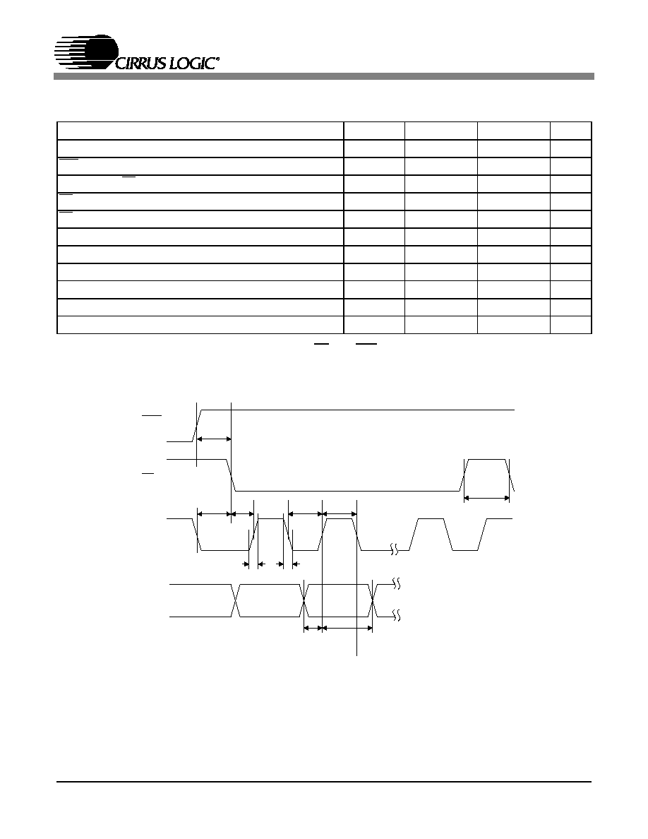
SWITCHING CHARACTERISTICS - PCM
( Inputs: Logic 0 = GND, Logic 1 = VLS, C
L
= 30pF)
Notes: 14. After powering up, RST should be held low until after the power supplies and clocks are settled.
15. See Tables 1 - 3 on page 18 for suggested MCLK frequencies.
Parameters Symbol
Min
Max
Units
RST pin Low Pulse Width
(Note 14)
1
-
ms
MCLK Frequency
1.024
55.2
MHz
MCLK Duty Cycle
(Note 15)
45
55
%
Input Sample Rate - LRCK (Manual selection)
Single-Speed Mode
Double-Speed Mode
Quad-Speed Mode
F
s
F
s
F
s
4
50
100
54
108
216
kHz
kHz
kHz
Input Sample Rate - LRCK (Auto detect)
Single-Speed Mode
Double-Speed Mode
Quad-Speed Mode
Fs
Fs
Fs
4
84
170
54
108
216
kHz
kHz
kHz
LRCK Duty Cycle
45
55
%
SCLK Duty Cycle
45
55
%
SCLK High Time
t
sckh
8
-
ns
SCLK Low Time
t
sckl
8
-
ns
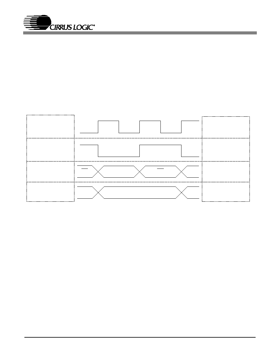
LRCK Edge to SCLK Rising Edge
t
lcks
5
-
ns
SCLK Rising Edge to LRCK Falling Edge
t
lckd
5
-
ns
SDIN Setup Time Before SCLK Rising Edge
t
ds
3
-
ns
SDIN Hold Time After SCLK Rising Edge
t
dh
5
-
ns
sckh
sckl
t
t
SD IN 1
dh
t
ds
t
lcks
t
lckd
t
SCLK
LRCK
lcks
t
M S B
M SB-1
SDINx
t
ds
SCLK
LRCK
MSB
t
dh
t
sckh
t
sckl
t
lcks
MSB-1
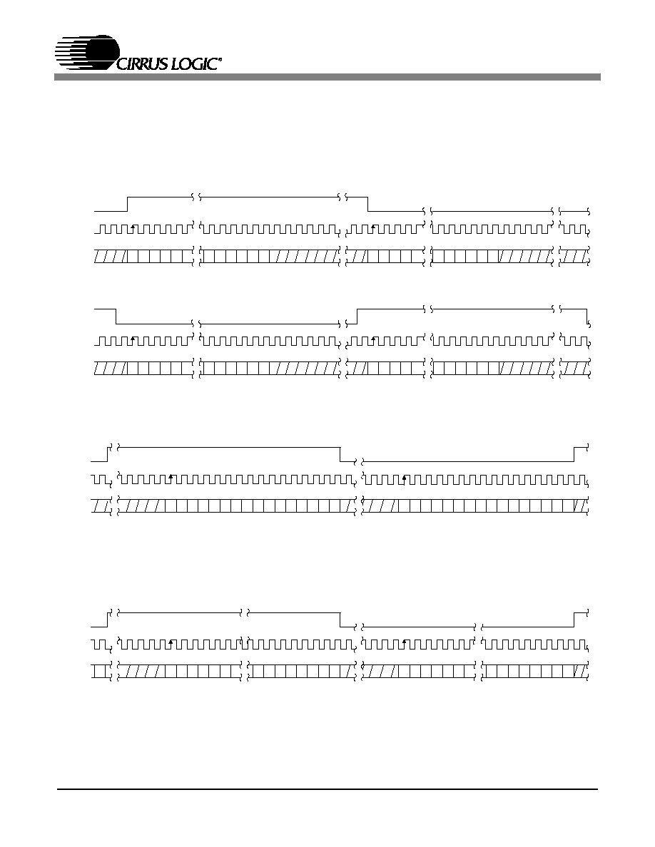
Figure 1. Serial Audio Interface Timing
Figure 2. TDM Serial Audio Interface Timing
CS4385
DS671A1
13
SWITCHING CHARACTERISTICS - DSD
(Logic 0 = AGND = DGND; Logic 1 = VLS Volts;
C
L
= 20 pF)
Parameter
Symbol Min Typ
Max
Unit
MCLK Duty Cycle
40
-
60
%
DSD_SCLK Pulse Width Low
t
sclkl
160
-
-
ns
DSD_SCLK Pulse Width High
t
sclkh
160
-
-
ns
DSD_SCLK Frequency (64x Oversampled)
(128x Oversampled)
1.024
2.048
-
-
3.2
6.4
MHz
MHz
DSD_A / _B valid to DSD_SCLK rising setup time
t
sdlrs
20
-
-
ns
DSD_SCLK rising to DSD_A or DSD_B hold time
t
sdh
20
-
-
ns
DSD clock to data transition (Phase Modulation mode)
t
dpm
-20
-
20
ns
sclkh
t
sclkl
t
DSDxx
DSD_SCLK
sdlrs
t
sdh
t
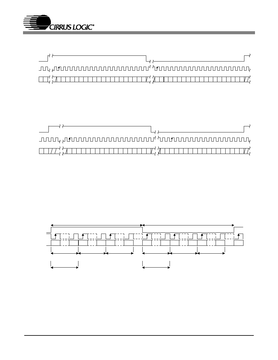
Figure 3. Direct Stream Digital - Serial Audio Input Timing
dpm
t
DSDxx
DSD_SCLK
(64Fs)
DSD_SCLK
(128Fs)
dpm
t
Figure 4. Direct Stream Digital - Serial Audio Input Timing for
Phase Modulation mode
CS4385
14
DS671A1
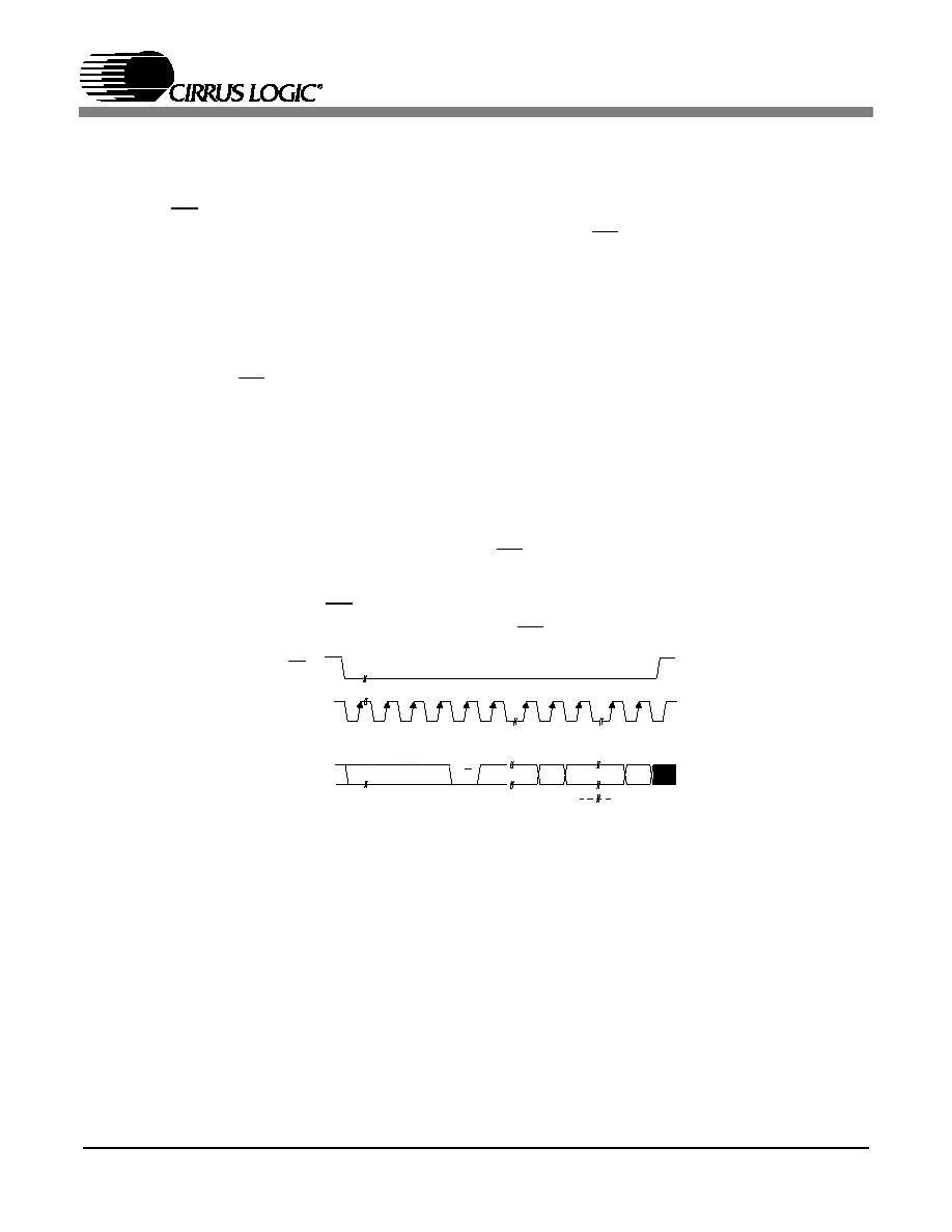
SWITCHING CHARACTERISTICS - CONTROL PORT - I
2
C FORMAT
(Inputs: Logic 0 = GND, Logic 1 = VLC, C
L
= 30 pF)
Notes: 16. Data must be held for sufficient time to bridge the transition time, t
fc
, of SCL.
Parameter
Symbol
Min
Max
Unit
SCL Clock Frequency
f
scl
-
100
kHz
RST Rising Edge to Start
t
irs
500
-
ns
Bus Free Time Between Transmissions
t
buf
4.7
-
�s
Start Condition Hold Time (prior to first clock pulse)
t
hdst
4.0
-
�s
Clock Low time
t
low
4.7
-
�s
Clock High Time
t
high
4.0
-
�s
Setup Time for Repeated Start Condition
t
sust
4.7
-
�s
SDA Hold Time from SCL Falling (Note 16)
t
hdd
0
-
�s
SDA Setup time to SCL Rising
t
sud
250
-
ns
Rise Time of SCL and SDA
t
rc
, t
rc
-
1
�s
Fall Time SCL and SDA
t
fc
, t
fc
-
300
ns
Setup Time for Stop Condition
t
susp
4.7
-
�s
Acknowledge Delay from SCL Falling
t
ack
300
1000
ns
t
buf
t
hdst
t
hdst
t
lo w
t r
t f
t
hdd
t
high
t sud
t sust
t susp
Stop
S ta rt
S ta rt
Stop
R e p e a te d
S D A
S C L
t
irs
R S T
Figure 5. Control Port Timing - I
2
C Format
CS4385
DS671A1
15
SWITCHING CHARACTERISTICS - CONTROL PORT - SPI FORMAT
(Inputs: Logic 0 = GND, Logic 1 = VLC, C
L
= 30 pF)
Notes: 17. t
spi
only needed before first falling edge of CS after RST rising edge. t
spi
= 0 at all other times.
18. Data must be held for sufficient time to bridge the transition time of CCLK.
19. For F
SCK
< 1 MHz.
Parameter
Symbol
Min
Max
Unit
CCLK Clock Frequency
f
sclk
-
6
MHz
RST Rising Edge to CS Falling
t
srs
500
-
ns
CCLK Edge to CS Falling (Note 17)
t
spi
500
-
ns
CS High Time Between Transmissions
t
csh
1.0
-
�s
CS Falling to CCLK Edge
t
css
20
-
ns
CCLK Low Time
t
scl
66
-
ns
CCLK High Time
t
sch
66
-
ns
CDIN to CCLK Rising Setup Time
t
dsu
40
-
ns
CCLK Rising to DATA Hold Time (Note 18)
t
dh
15
-
ns
Rise Time of CCLK and CDIN (Note 19)
t
r2
-
100
ns
Fall Time of CCLK and CDIN (Note 19)
t
f2
-
100
ns
t r2
t f2
t dsu t
dh
t
s ch
t scl
C S
C C L K
C D IN
t css
t
c sh
t spi
t srs
R S T
Figure 6. Control Port Timing - SPI Format
CS4385
16
DS671A1
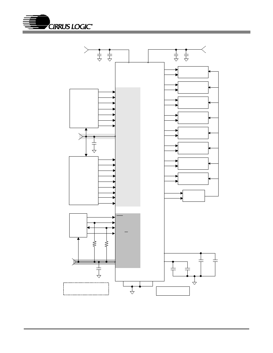
Digital
Audio
Source
VLS
MCLK
VD
AOUTA1+
8
32
0.1 �F
+
1 �F
+2.5 V
SDIN1
9
1 �F
0.1 �F
+
+
20
21
FILT+
VQ
7
6
LRCK
SCLK
SDIN3
SDIN2
39
40
0.1 �F
47 �F
VA
0.1 �F
+
1 �F
0.1 �F
+1.8 V to +5 V
+5 V
4
43
SDIN4
13
14
Analog Conditioning
and Muting
AOUTA1-
AOUTB1+ 38
37
Analog Conditioning
and Muting
AOUTB1-
AOUTA2+
35
36
Analog Conditioning
and Muting
AOUTA2-
AOUTB2+ 34
33
Analog Conditioning
and Muting
AOUTB2-
AOUTA3+
29
30
Analog Conditioning
and Muting
AOUTA3-
AOUTB3+
28
27
Analog Conditioning
and Muting
AOUTB3-
AOUTA4+ 25
26
Analog Conditioning
and Muting
AOUTA4-
AOUTB4+
24
23
Analog Conditioning
and Muting
AOUTB4-
MUTEC1 41
22
Mute
Drive
MUTEC234
11
PCM
Micro-
Controller
VLC
0.1 �F
+1.8 V to +5 V
18
DSD
Audio
Source
2
48
DSDB2
3
42
DSD_SCLK
DSDA1
DSDB3
DSDA3
DSDA4
DSDB1
DSDA2
46
45
47
1
44
DSDB4
16
15
SCL/CCLK
SDA/CDIN
ADO/CS
RST
19
17
2 K
2 K
Note: Necessary for I
2
C
control port operation
Note*
CS4385
31
GND
GND
5
Note
TST
: Pins 10, 12
TST*
Figure 7. Typical Connection Diagram, Software Mode

CS4385
DS671A1
17
Digital
Audio
Source
VLS
CS4385
MCLK
VD
AOUTA1+
8
32
0.1 �F
+
1 �F
+2.5 V
SDIN1
9
1 �F
0.1 �F
+
+
20
21
FILT+
VQ
7
6
LRCK
SCLK
SDIN3
SDIN2
39
40
0.1 �F
47 �F
VA
0.1 �F
+
1 �F
0.1 �F
+1.8 V to +5 V
+5 V
4
43
SDIN4
13
14
Analog Conditioning
and Muting
AOUTA1-
AOUTB1+ 38
37
Analog Conditioning
and Muting
AOUTB1-
AOUTA2+
35
36
Analog Conditioning
and Muting
AOUTA2-
AOUTB2+ 34
33
Analog Conditioning
and Muting
AOUTB2-
AOUTA3+ 29
30
Analog Conditioning
and Muting
AOUTA3-
AOUTB3+
28
27
Analog Conditioning
and Muting
AOUTB3-
AOUTA4+ 25
26
Analog Conditioning
and Muting
AOUTA4-
AOUTB4+
24
23
Analog Conditioning
and Muting
AOUTB4-
MUTEC234
22
41
Mute
Drive
MUTEC1
11
PCM
31
GND
GND
5
Stand-Alone
Mode
Configuration
VLC
0.1 �F
+1.8 V to +5 V
18
DSD
Audio
Source
2
48
DSDB2
3
12
M3
DSDA1
DSDB3
DSDA3
DSDA4
DSDB1
DSDA2
46
45
47
1
44
DSDB4
16
15
M2
M1
M0
RST
19
17
Mute
Drive
47 K
Optional
42
DSD_SCLK
10
M4
Figure 8. Typical Connection Diagram, Hardware
CS4385
18
DS671A1
3. APPLICATIONS
The CS4385 serially accepts twos complement formatted PCM data at standard audio sample
rates including 48, 44.1 and 32 kHz in SSM, 96, 88.2 and 64 kHz in DSM, and 192, 176.4 and
128 kHz in QSM. Audio data is input via the serial data input pins (SDINx). The Left/Right Clock
(LRCK) determines which channel is currently being input on SDINx, and the Serial Clock
(SCLK) clocks audio data into the input data buffer.
The CS4385 can be configured in hardware mode by the M0, M1, M2 , M3 and M4 pins and in
software mode through I
2
C or SPI.
3.1
Master Clock
MCLK/LRCK must be an integer ratio as shown in Tables 1 - 3. The LRCK frequency is equal to
Fs, the frequency at which words for each channel are input to the device. The MCLK-to-LRCK
frequency ratio and speed mode is detected automatically during the initialization sequence by
counting the number of MCLK transitions during a single LRCK period and by detecting the ab-
solute speed of MCLK. Internal dividers are then set to generate the proper internal clocks. Ta-
bles 1 - 3 illustrate several standard audio sample rates and the required MCLK and LRCK
frequencies. Please note there is no required phase relationship, but MCLK, LRCK and SCLK
must be synchronous.
Sample Rate
(kHz)
MCLK (MHz)
256x
384x
512x
768x
1024x
1152x
32
8.1920
12.2880
16.3840
24.5760
32.7680
36.8640
44.1
11.2896
16.9344
22.5792
33.8688
45.1584
48
12.2880
18.4320
24.5760
36.8640
49.1520
Table 1. Single-Speed Mode Standard Frequencies
Sample Rate
(kHz)
MCLK (MHz)
128x
192x
256x
384x
512x
64
8.1920
12.2880
16.3840
24.5760
32.7680
88.2
11.2896
16.9344
22.5792
33.8688
45.1584
96
12.2880
18.4320
24.5760
36.8640
49.1520
Table 2. Double-Speed Mode Standard Frequencies
Sample Rate
(kHz)
MCLK (MHz)
64x
96x
128x
192x
256x
176.4
11.2896
16.9344
22.5792
33.8688
45.1584
192
12.2880
18.4320
24.5760
36.8640
49.1520
Table 3. Quad-Speed Mode Standard Frequencies
= Denotes clock ratio and sample rate combinations which are NOT supported under auto
speed-mode detection. Please see "Switching Characteristics - PCM" on page 12.
CS4385
DS671A1
19
3.2
Mode Select
In hardware mode operation is determined by the Mode Select pins. The state of these pins are
continually scanned for any changes. These pins require connection to supply or ground as out-
lined in figure 8. For M0, M1, M2 supply is VLC and for M3 and M4 supply is VLS. Tables 4 - 6
show the decode of these pins.
In software mode the operational mode and data format are set in the FM and DIF registers.
See "Register Description" on page 37.
M1
(DIF1)
M0
(DIF0)
DESCRIPTION
FORMAT
FIGURE
0
0
Left Justified, up to 24-bit data
0
9
0
1
I
2
S, up to 24-bit data
1
10
1
0
Right Justified, 16-bit Data
2
11
1
1
Right Justified, 24-bit Data
3
12
Table 4. PCM Digital Interface Format, Hardware Mode Options
M4
M3
M2
(DEM)
DESCRIPTION
0
0
0
Single-Speed without De-Emphasis (4 to 50 kHz sample rates)
0
0
1
Single-Speed with 44.1kHz De-Emphasis; see Figure 20
0
1
0
Double-Speed (50 to 100 kHz sample rates)
0
1
1
Quad-Speed (100 to 200 kHz sample rates)
1
0
0
Auto Speed-Mode Detect (32kHz to 200kHz sample rates)
1
0
1
Auto Speed-Mode Detect with 44.1kHz De-Emphasis; see Figure 20
1
1
X
DSD Processor Mode (see Table 6 for details)
Table 5. Mode Selection, Hardware Mode Options
M2
M1
M0
DESCRIPTION
0
0
0
64x oversampled DSD data with a 4x MCLK to DSD data rate
0
0
1
64x oversampled DSD data with a 6x MCLK to DSD data rate
0
1
0
64x oversampled DSD data with a 8x MCLK to DSD data rate
0
1
1
64x oversampled DSD data with a 12x MCLK to DSD data rate
1
0
0
128x oversampled DSD data with a 2x MCLK to DSD data rate
1
0
1
128x oversampled DSD data with a 3x MCLK to DSD data rate
1
1
0
128x oversampled DSD data with a 4x MCLK to DSD data rate
1
1
1
128x oversampled DSD data with a 6x MCLK to DSD data rate
Table 6. Direct Stream Digital (DSD), Hardware Mode Options
CS4385
20
DS671A1
3.3
Digital Interface Formats
The serial port operates as a slave and supports the I�S, Left-Justified, Right-Justified, One-Line
Mode (OLM) and TDM digital interface formats with varying bit depths from 16 to 32 as shown in
Figures 9-19. Data is clocked into the DAC on the rising edge. OLM and TDM configurations are
only supported in software mode.
LRCK
SCLK
Left Channel
Right Channel
SDINx
+3 +2 +1
+5 +4
-1 -2 -3 -4 -5
+3 +2 +1
+5 +4
-1 -2 -3 -4
MSB
LSB
MSB
LSB
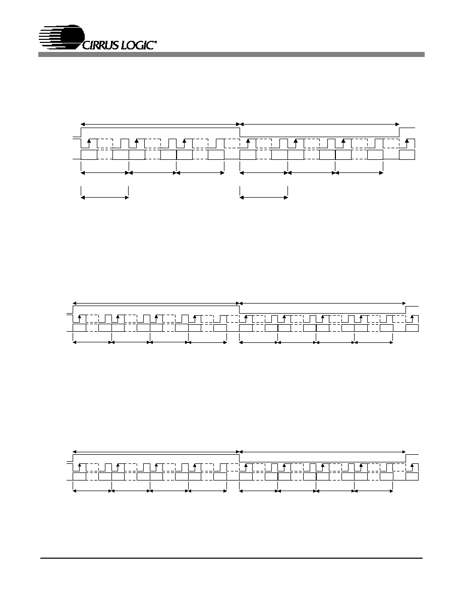
Figure 9. Format 0 - Left Justified up to 24-bit Data
LRCK
SCLK
Left Channel
Right Channel
SDINx
+3 +2 +1
+5 +4
-1 -2 -3 -4 -5
+3 +2 +1
+5 +4
-1 -2 -3 -4
MSB
MSB
LSB
LSB
Figure 10. Format 1 - I
2
S up to 24-bit Data
LRCK
SCLK
Left Channel
Right Channel
SDINx
6
5
4
3
2
1
0
9
8
7
15 14 13 12 11 10
6
5
4
3
2
1
0
9
8
7
15 14 13 12 11 10
32 clocks
Figure 11. Format 2 - Right Justified 16-bit Data
LRCK
SCLK
Left Channel
SDINx
6
5
4
3
2
1
0
7
23 22 21 20 19 18
6
5
4
3
2
1
0
7
23 22 21 20 19 18
32 clocks
0
Right Channel
Figure 12. Format 3 - Right Justified 24-bit Data
CS4385
DS671A1
21
3.3.1
OLM #1
OLM #1 serial audio interface format operates in single, double, or quad-speed mode and
will slave to SCLK at 128 Fs. Six channels of MSB first 20-bit PCM data are input on
SDIN1. The last two channels are input on SDIN4.
LRCK
SCLK
Left Channel
Right Channel
SDINx
6
5
4
3
2
1
0
9
8
7
15 14 13 12 11 10
1
0
6
5
4
3
2
1
0
9
8
7
15 14 13 12 11 10
17 16
17 16
32 clocks
19 18
19 18
Figure 13. Format 4 - Right Justified 20-bit Data
LRCK
SCLK
Left Channel
Right Channel
SDINx
6
5
4
3
2
1
0
9
8
7
15 14 13 12 11 10
1
0
6
5
4
3
2
1
0
9
8
7
15 14 13 12 11 10
17 16
17 16
32 clocks
Figure 14. Format 5 - Right Justified 18-bit Data
LRCK
SCLK
LSB
MSB
20 clks
64 clks
64 clks
LSB
MSB
LSB
MSB
LSB
MSB
LSB
MSB
LSB
MSB
MSB
DAC_A1
20 clks
20 clks
20 clks
20 clks
20 clks
Left Channel
Right Channel
20 clks
20 clks
SDIN4
SDIN1
DAC_A2
DAC_A3
DAC_A4
DAC_B1
DAC_B4
DAC_B2
DAC_B3
Figure 15. Format 8 - One Line Mode 1
CS4385
22
DS671A1
3.3.2
OLM #2
OLM #2 serial audio interface format operates in single, double, or quad-speed mode and
will slave to SCLK at 256 Fs. Six channels of MSB first 24-bit PCM data are input on
SDIN1. The last two channels are input on SDIN4.
3.3.3
OLM #3
OLM #3 serial audio interface format operates in single, double, or quad-speed mode and
will slave to SCLK at 256 Fs. Eight channels of MSB first 20-bit PCM data are input on
SDIN1.
3.3.4
OLM #4
OLM #4 serial audio interface format operates in single, double, or quad-speed mode and
will slave to SCLK at 256 Fs. Eight channels of MSB first 24-bit PCM data are input on
SDIN1.
LSB
MSB
24 clks
128 clks
LSB
MSB
LSB
MSB
LSB
MSB
LSB
MSB
LSB
MSB
MSB
DAC_A1
24 clks
24 clks
24 clks
24 clks
24 clks
Left Channel
Right Channel
24 clks
24 clks
128 clks
LRCK
SCLK
SDIN1
SDIN4
DAC_A4
DAC_A2
DAC_A3
DAC_B1
DAC_B2
DAC_B3
DAC_B4
Figure 16. Format 9 - One Line Mode 2
LSB
MSB
20 clks
128 clks
LSB
MSB
LSB
MSB
LSB
MSB
LSB
MSB
LSB
MSB
MSB
DAC_A1
20 clks
20 clks
20 clks
20 clks
20 clks
Left Channel
Right Channel
128 clks
LRCK
SCLK
SDIN1
DAC_A2
DAC_A3
DAC_B1
DAC_B2
DAC_B3
LSB
MSB
20 clks
DAC_A4
LSB
MSB
20 clks
DAC_B4
Figure 17. Format 10 - One Line Mode 3
LSB
MSB
24 clks
128 clks
LSB
MSB
LSB
MSB
LSB
MSB
LSB
MSB
LSB
MSB
MSB
DAC_A1
24 clks
24 clks
24 clks
24 clks
24 clks
Left Channel
Right Channel
128 clks
LRCK
SCLK
SDIN1
DAC_A2
DAC_A3
DAC_B1
DAC_B2
DAC_B3
LSB
MSB
24 clks
DAC_A4
LSB
MSB
24 clks
DAC_B4
Figure 18. Format 11 - One Line Mode 4

CS4385
DS671A1
23
3.3.5
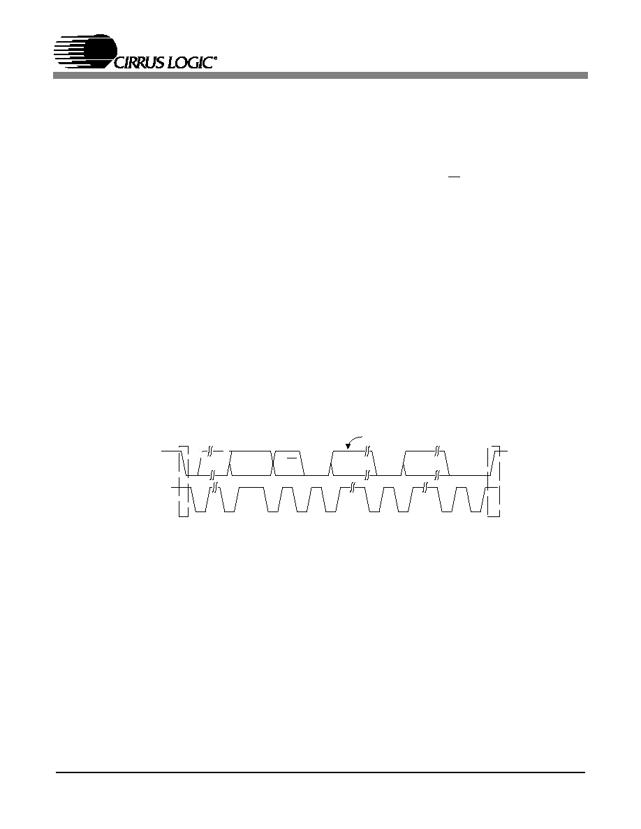
TDM
The TDM serial audio interface format operates in single, double, or quad-speed mode
and will slave to SCLK at 256 Fs. Data is received most significant bit first on the first
SCLK after an LRCK transition and is valid on the rising edge of SCLK. LRCK identifies
the start of a new frame and is equal to the sample rate, Fs. LRCK is sampled as valid on
the rising SCLK edge preceding the most significant bit of the first data sample and must
be held valid for one SCLK period. Each time slot is 32 bits wide, with the valid data sam-
ple left justified within the time slot with the remaining bits being zero padded.
3.4
Oversampling Modes
The CS4385
operates in one of three oversampling modes based on the input sample rate. Mode
selection is determined by the M4, M3 and M2 pins in hardware mode or the FM bits in software
mode. Single-Speed mode supports input sample rates up to 50 kHz and uses a 128x oversam-
pling ratio. Double-Speed mode supports input sample rates up to 100 kHz and uses an over-
sampling ratio of 64x. Quad-speed mode supports input sample rates up to 200 kHz and uses
an oversampling ratio of 32x.
The auto-speed mode detect feature allows for the automatic selection of speed mode based off
of the incoming sample rate. This allows the CS4385 to accept a wide range of sample rates
with no external intervention necessary. The auto-speed mode detect feature is available in both
hardware and software mode.
3.5
Interpolation Filter
To accommodate the increasingly complex requirements of digital audio systems, the CS4385
incorporates selectable interpolation filters for each mode of operation. A "fast" and a "slow" roll-
off filter is available in each of Single, Double, and Quad Speed modes. These filters have been
designed to accommodate a variety of musical tastes and styles. The FILT_SEL bit is used to
select which filter is used (see the Register Description section for more details).
When in hardware mode, only the "fast" roll-off filter is available.
Filter specifications can be found in Section 2, and filter response plots can be found in Figures
28 to
51.
DAC_B2
LRCK
SCLK
LSB
MSB
LSB
MSB
LSB
MSB
LSB
MSB
LSB
MSB
SDIN1
DAC_A1
DAC_A2
DAC_B1
DAC_A3
256 clks
32 clks
32 clks
32 clks
32 clks
32 clks
LSB
MSB
DAC_B3
32 clks
LSB
MSB
DAC_A4
32 clks
LSB
MSB
DAC_B4
32 clks
LSB
LSB
MSB
zero
Data
Figure 19. Format 12 - TDM Mode
CS4385
24
DS671A1
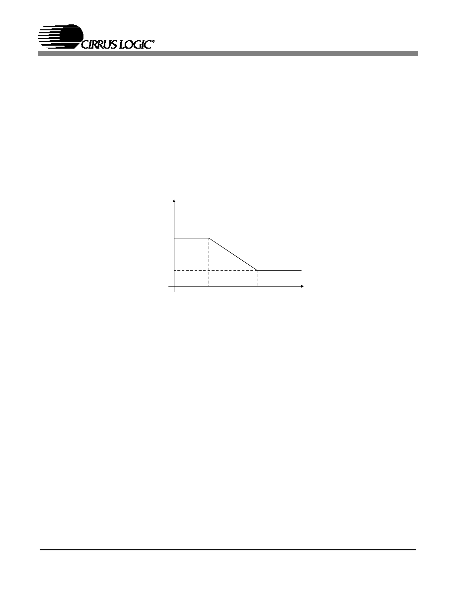
3.6
De-Emphasis
The CS4385 includes on-chip digital de-emphasis filters. The de-emphasis feature is included to
accommodate older audio recordings that utilize pre-emphasis equalization as a means of noise
reduction. Figure 20 shows the de-emphasis curve. The frequency response of the de-emphasis
curve will scale proportionally with changes in sample rate, Fs if the input sample rate does not
match the coefficient which has been selected.
In software mode the required de-emphasis filter coefficients for 32 kHz, 44.1 kHz, or 48 kHz are
selected via the de-emphasis control bits.
In hardware mode only the 44.1 kHz coefficient is available (enabled through the M2 pin). If the
input sample rate is not 44.1 kHz and de-emphasis has been selected then the corner frequen-
cies of the de-emphasis filter will be scaled by a factor of the actual Fs over 44,100.
Gain
dB
-10dB
0dB
Frequency
T2 = 15 �s
T1=50 �s
F1
F2
3.183 kHz
10.61 kHz
Figure 20. De-Emphasis Curve
CS4385
DS671A1
25
3.7
ATAPI Specification
The CS4385 implements the channel mixing functions of the ATAPI CD-ROM specification. The
ATAPI functions are applied per A-B pair. Refer to Table 9 on page 46 and Figure 21 for addi-
tional information.
3.8
Direct Stream Digital (DSD) Mode
In software mode the DSD/PCM bits (Reg. 02h) are used to configure the device for DSD mode.
The DSD_DIF bits (Reg 04h) then control the expected DSD rate and MCLK ratio.
The DIR_DSD bit (Reg 04h) selects between two proprietary methods for DSD to analog conver-
sion. The first method uses a decimation free DSD processing technique which allows for fea-
tures such as matched PCM level output, DSD volume control, and 50kHz on chip filter. The
second method sends the DSD data directly to the on-chip switched-capacitor filter for conver-
sion (without the above mentioned features).
The DSD_PM_EN bit (Reg. 04h) selects Phase Modulation (data plus data inverted) as the style
of data input. In this mode the DSD_PM_mode bit selects whether a 128Fs or 64x clock is used
for phase modulated 64x data (see Figure 22). Use of phase modulation mode may not directly
effect the performance of the CS4385, but may lower the sensitivity to board level routing of the
DSD data signals.
The CS4385 can detect errors in the DSD data which does not comply with the SACD specifica-
tion. The STATIC_DSD and INVALID_DSD bits (Reg. 04h) allow the CS4385 to alter the incom-
ing invalid DSD data. Depending on the error, the data may either be attenuated or replaced with
a muted DSD signal (the MUTEC pins would be set according to the DAMUTE bit (Reg. 08h)).
A Channel
Volume
Control
Aout Ax
AoutBx
Left Chan
nel
Audio D
ata
Right Chan
nel
Audio D
ata
B Channel
Volume
Control
MUTE
MUTE
SDINx
Figure 21. ATAPI Block Diagram (x = channel pair 1, 2, 3, or 4)
CS4385
26
DS671A1
More information for any of these register bits can be found in the Register Description section.
The DSD input structure and analog outputs are designed to handle a nominal 0 dB-SACD (50%
modulation index) at full rated performance. Signals of +3 dB-SACD may be applied for brief pe-
riods of time however, performance at these levels is not guaranteed. If sustained +3 dB-SACD
levels are required, the digital volume control should be set to -3.0 dB. This same volume control
register affects PCM output levels. There is no need to change the volume control setting be-
tween PCM and DSD in order to have the 0dB output levels match (both 0 dBFS and 0 dB-SACD
will output at -3 dB in this case).
Figure 22. DSD phase modulation mode diagram
3.9
Grounding and Power Supply Arrangements
As with any high resolution converter, the CS4385 requires careful attention to power supply and
grounding arrangements if its potential performance is to be realized. The Typical Connection Di-
agram shows the recommended power arrangements, with VA, VD, VLC, and VLS connected to
clean supplies. If the ground planes are split between digital ground and analog ground, the GND
pins of the CS4385 should be connected to the analog ground plane.
All signals, especially clocks, should be kept away from the FILT+ and VQ pins in order to avoid
unwanted coupling into the DAC.
BCKA
(128Fs)
BCKD
(64Fs)
DSD_SCLK
DSDAx,
DSDBx
D1
D1
D1
D0
D2
D2
D0
DSD_SCLK
DSDAx,
DSDBx
BCKA
(64Fs)
DSD_SCLK
DSD Phase
Modulation Mode
DSD Normal Mode
Not Used
Not Used
Not Used
CS4385
DS671A1
27
3.9.1
Capacitor Placement
Decoupling capacitors should be placed as close to the DAC as possible, with the low val-
ue ceramic capacitor being the closest. To further minimize impedance, these capacitors
should be located on the same layer as the DAC. If desired, all supply pins with similar
voltage ratings may be connected to the same supply, but a decoupling capacitor should
still be placed on each supply pin.
Note: All decoupling capacitors should be referenced to analog ground.
The CDB4385 evaluation board demonstrates the optimum layout and power supply ar-
rangements.
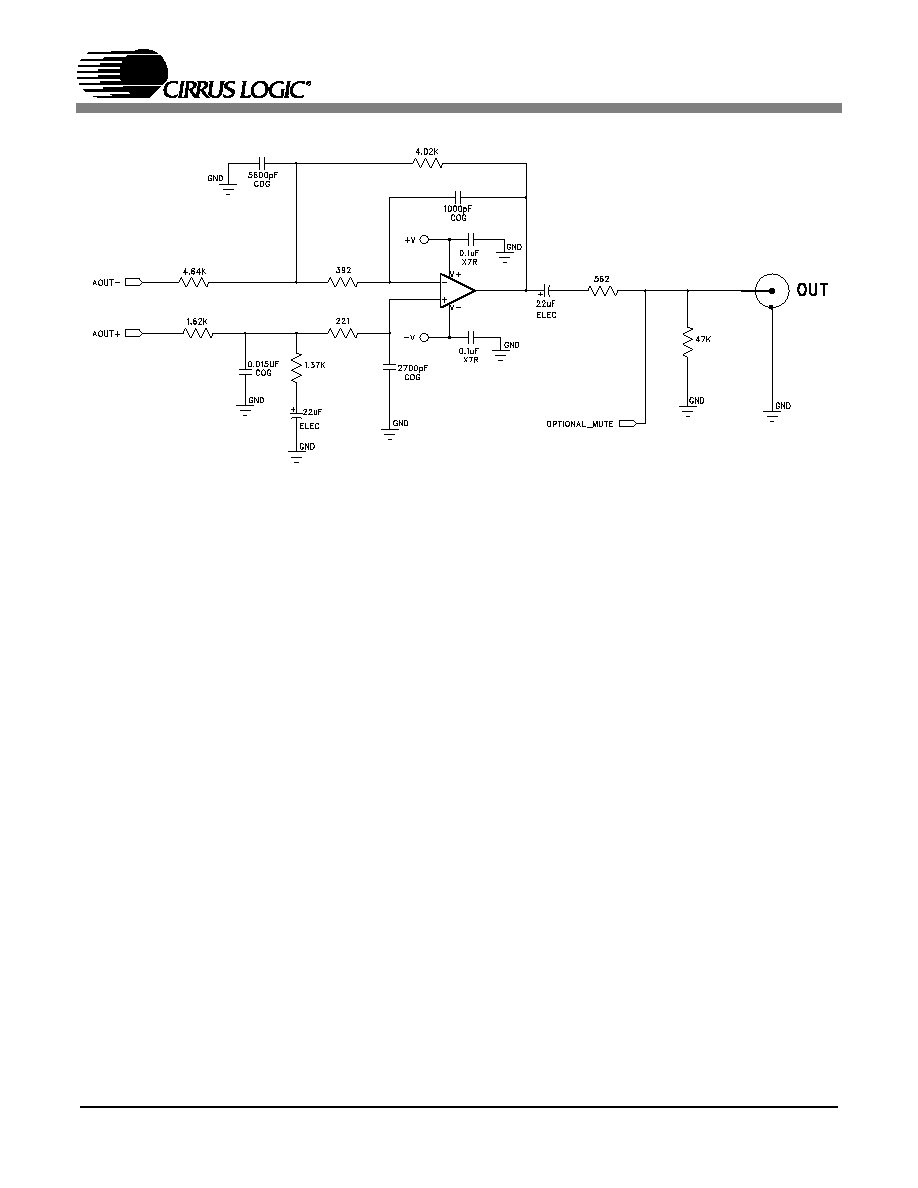
3.10 Analog Output and Filtering
The application note "Design Notes for a 2-Pole Filter with Differential Input" discusses the sec-
ond-order Butterworth filter and differential to single-ended converter which was implemented on
the
CS4385
evaluation board, CDB4385 Evaluation Board, as seen in Figure 24. The CS4385
does not include phase or amplitude compensation for an external filter. Therefore, the DAC sys-
tem phase and amplitude response will be dependent on the external analog circuitry. The off-
chip filter has been designed to attenuate the typical full-scale output level to below 2 Vrms.
Figure 23 shows how the full-scale differential analog output level specification is derived.
AOUT+
AOUT-
Full-Scale Output Level= (AOUT+) - (AOUT-)= 6.7 Vpp
3.85 V
2.5 V
1.15 V
3.85 V
2.5 V
1.15 V
Figure 23. Full-Scale Output
CS4385
28
DS671A1
Figure 24. Recommended Output Filter
CS4385
DS671A1
29
3.11 The MUTEC Outputs
The MUTEC1 and MUTEC234 pins have an auto-polarity detect feature. The MUTEC output pins
are high impedance at the time of reset. The external mute circuitry needs to be self biased into
an active state in order to be muted during reset. Upon release of reset, the CS4385 will detect
the status of the MUTEC pins (high or low) and will then select that state as the polarity to drive
when the mutes become active. The external-bias voltage level that the MUTEC pins see at the
time of release of reset must meet the "MUTEC auto detect input high/low voltage" specs as out-
lined in the Digital Characteristics section.
Figure 25 shows a single example of both an active high and an active low mute drive circuit. In
these designs, the pull-up and pull-down resistors have been especially chosen to meet the input
high/low threshold when used with the MMUN2111 and MMUN2211 internal bias resistances of
10 k
.
Use of the Mute Control function is not mandatory but recommended for designs requiring the
absolute minimum in extraneous clicks and pops. Also, use of the Mute Control function can en-
able the system designer to achieve idle channel noise/signal-to-noise ratios which are only lim-
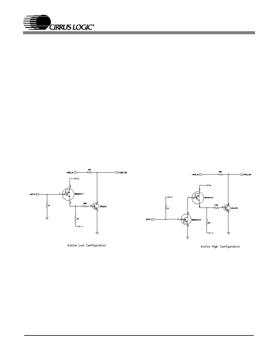
ited by the external mute circuit.
Figure 25. Recommended Mute Circuitry

CS4385
30
DS671A1
3.12 Recommended Power-up Sequence
3.12.1 Hardware Mode
1. Hold RST low until the power supplies and configuration pins are stable, and the master
and left/right clocks are locked to the appropriate frequencies, as discussed in section 3.1.
In this state, the registers are reset to the default settings, FILT+ will remain low, and VQ
will be connected to VA/2.
If RST can not be held low long enough the SDINx pins should remain static low until all
other clocks are stable, and if possible the RST should be toggled low again once the sys-
tem is stable.
2. Bring RST high. The device will remain in a low power state with FILT+ low and will ini-
tiate the Hardware power-up sequence after approximately 512 LRCK cycles in Single-
Speed Mode (1024 LRCK cycles in Double-Speed Mode, and 2048 LRCK cycles in Quad-
Speed Mode).
3.12.2 Software Mode
1. Hold RST low until the power supply is stable, and the master and left/right clocks are
locked to the appropriate frequencies, as discussed in section 3.1. In this state, the regis-
ters are reset to the default settings, FILT+ will remain low, and VQ will be connected to
VA/2.
2. Bring RST high. The device will remain in a low power state with FILT+ low for 512
LRCK cycles in Single-Speed Mode (1024 LRCK cycles in Double-Speed Mode, and 2048
LRCK cycles in Quad-Speed Mode).
3. In order to reduce the chances of clicks and pops, perform a write to the CP_EN bit prior
to the completion of approximately 512 LRCK cycles in Single-Speed Mode (1024 LRCK
cycles in Double-Speed Mode, and 2048 LRCK cycles in Quad-Speed Mode). The de-
sired register settings can be loaded while keeping the PDN bit set to 1.
If more than the stated number of LRCK cycles passes before CPEN bit is written then the
chip will enter Hardware mode and begin to operate with the M0-M4 as the mode settings.
CPEN bit may be written at anytime, even after the Hardware sequence has begun. It is
advised that if the CPEN bit can not be set in time then the SDINx pins should remain stat-
ic low (this way no audio data can be converted incorrectly by the hardware mode set-
tings).
4. Set the PDN bit to 0. This will initiate the power-up sequence, which lasts approximately
50 �s.

CS4385
DS671A1
31
3.13 Control Port Interface
The control port is used to load all the internal register settings in order to operate in software
mode (see section 5). The operation of the control port may be completely asynchronous with
the audio sample rate. However, to avoid potential interference problems, the control port pins
should remain static if no operation is required.
The control port operates in one of two modes: I
2
C or SPI.
3.13.1 MAP Auto Increment
The device has MAP (memory address pointer) auto increment capability enabled by the
INCR bit (also the MSB) of the MAP. If INCR is set to 0, MAP will stay constant for suc-
cessive I
2
C writes or reads and SPI writes. If INCR is set to 1, MAP will auto increment
after each byte is written, allowing block reads or writes of successive registers.
3.13.2 I
2
C Mode
In the I
2
C mode, data is clocked into and out of the bi-directional serial control data line,
SDA, by the serial control port clock, SCL (see Figure 26 for the clock to data relationship).
There is no CS pin. Pin AD0 enables the user to alter the chip address
(001100[AD0][R/W]) and should be tied to VLC or GND as required, before powering up
the device. If the device ever detects a high to low transition on the AD0/CS pin after pow-
er-up, SPI mode will be selected.
3.13.2.1 I
2
C Write
To write to the device, follow the procedure below while adhering to the control port
Switching Specifications in section 2.
1) Initiate a START condition to the I
2
C bus followed by the address byte. The upper
6 bits must be 001100. The seventh bit must match the setting of the AD0 pin, and the
eighth must be 0. The eighth bit of the address byte is the R/W bit.
2) Wait for an acknowledge (ACK) from the part, then write to the memory address
pointer, MAP. This byte points to the register to be written.
3) Wait for an acknowledge (ACK) from the part, then write the desired data to the reg-
ister pointed to by the MAP.
4) If the INCR bit (see section 3.13.1) is set to 1, repeat the previous step until all the
desired registers are written, then initiate a STOP condition to the bus.
5) If the INCR bit is set to 0 and further I
2
C writes to other registers are desired, it is
necessary to initiate a repeated START condition and follow the procedure detailed
from step 1. If no further writes to other registers are desired, initiate a STOP condition
to the bus.
CS4385
32
DS671A1
3.13.2.2 I
2
C Read
To read from the device, follow the procedure below while adhering to the control port
Switching Specifications.
1) Initiate a START condition to the I
2
C bus followed by the address byte. The upper
6 bits must be 001100. The seventh bit must match the setting of the AD0 pin, and the
eighth must be 1. The eighth bit of the address byte is the R/W bit.
2) After transmitting an acknowledge (ACK), the device will then transmit the contents
of the register pointed to by the MAP. The MAP register will contain the address of the
last register written to the MAP, or the default address (see section 3.13.1) if an I
2
C
read is the first operation performed on the device.
3) Once the device has transmitted the contents of the register pointed to by the MAP,
issue an ACK.
4) If the INCR bit is set to 1, the device will continue to transmit the contents of succes-
sive registers. Continue providing a clock and issue an ACK after each byte until all the
desired registers are read, then initiate a STOP condition to the bus.
5) If the INCR bit is set to 0 and further I
2
C reads from other registers are desired, it is
necessary to initiate a repeated START condition and follow the procedure detailed
from steps 1 and 2 from the I
2
C Write instructions followed by step 1 of the I
2
C Read
section. If no further reads from other registers are desired, initiate a STOP condition
to the bus.
S D A
S C L
0 01 1 00
A D D R
AD 0
R /W
S ta rt
A C K
D AT A
1-8
A C K
D A TA
1-8
A C K
S top
N o te : If o p e ra tio n is a w rite , th is b y te c o n ta in s th e M e m o ry A d d re s s P o in te r, M A P .
N o te 1
Figure 26. Control Port Timing, I
2
C Mode
CS4385
DS671A1
33
3.13.3 SPI Mode
In SPI mode, data is clocked into the serial control data line, CDIN, by the serial control
port clock, CCLK (see Figure 27 for the clock to data relationship). There is no AD0 pin.
Pin CS is the chip select signal and is used to control SPI writes to the control port. When
the device detects a high to low transition on the AD0/CS pin after power-up, SPI mode
will be selected. All signals are inputs and data is clocked in on the rising edge of CCLK.
3.13.3.1 SPI Write
To write to the device, follow the procedure below while adhering to the control port
Switching Specifications in Section 2.
1) Bring CS low.
2) The address byte on the CDIN pin must then be 00110000.
3) Write to the memory address pointer, MAP. This byte points to the register to be writ-
ten.
4) Write the desired data to the register pointed to by the MAP.
5) If the INCR bit (see section 3.13.1) is set to 1, repeat the previous step until all the
desired registers are written, then bring CS high.
6) If the INCR bit is set to 0 and further SPI writes to other registers are desired, it is
necessary to bring CS high, and follow the procedure detailed from step 1. If no further
writes to other registers are desired, bring CS high.
M A P
M S B
LSB
D A TA
byte 1
byte n
R /W
M A P = M e m o ry A d d re s s P o in te r
A D D R E S S
C H IP
C D IN
C C L K
C S
0011000
Figure 27. Control Port Timing, SPI mode

CS4385
34
DS671A1
3.14 Memory Address Pointer (MAP)
3.14.1 INCR (AUTO MAP INCREMENT ENABLE)
Default = `0'
0 - Disabled
1 - Enabled
3.14.2 MAP4-0 (MEMORY ADDRESS POINTER)
Default = `00000'
7
6
5
4
3
2
1
0
INCR
Reserved
Reserved
MAP4
MAP3
MAP2
MAP1
MAP0
0
0
0
0
0
0
0
0
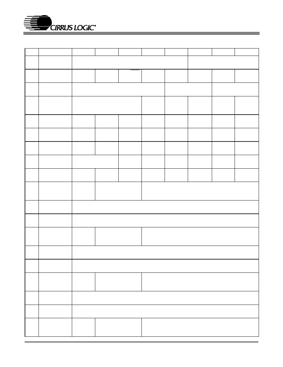
CS4385
DS671A1
35
4.
REGISTER QUICK REFERENCE
Addr
Function
7
6
5
4
3
2
1
0
01h Chip Revision
PART4
PART3
PART2
PART1
PART0
REV
REV
REV
default
0
0
0
0
1
x
x
x
02h Mode Control
CPEN
FREEZE
DSD/PCM DAC4_DIS DAC3_DIS DAC2_DIS DAC1_DIS
PDN
default
0
0
0
0
0
0
0
1
03h PCM Control
DIF3
DIF2
DIF1
DIF0
Reserved
Reserved
FM1
FM0
default
0
0
0
0
0
0
1
1
04h DSD Control
DSD_DIF2 DSD_DIF1 DSD_DIF0 DIR_DSD STATIC_D
SD
INVALID_D
SD
DSD_PM_
MD
DSD_PM_
EN
default
0
0
0
0
1
1
0
0
05h Filter Control
Reserved
Reserved
Reserved
Reserved
Reserved
Reserved
Reserved
FILT_SEL
default
0
0
0
0
0
0
0
0
06h Invert Control
INV_B4
INV_A4
INV_B3
INV_A3
INV_B2
INV_A2
INV_B1
INV_A1
default
0
0
0
0
0
0
0
0
07h Group Control
Reserved
MUTEC
Reserved
P1_A=B
P2_A=B
P3_A=B
P4_A=B
SNGLVOL
default
0
0
1
0
0
1
0
0
08h Ramp and Mute
SZC1
SZC0
RMP_UP
RMP_DN
PAMUTE
DAMUTE
MUTE_P1 MUTE_P0
default
1
0
0
0
0
0
0
0
09h Mute Control
MUTE_B4 MUTE_A4 MUTE_B3 MUTE_A3 MUTE_B2 MUTE_A2 MUTE_B1 MUTE_A1
default
0
0
0
0
0
0
0
0
0Ah Mixing Control
Pair 1 (AOUTx1)
Reserved
P1_DEM1 P1_DEM0 P1ATAPI4 P1ATAPI3
P1ATAPI2
P1ATAPI1
P1ATAPI0
default
0
0
1
0
1
0
0
1
0Bh Vol. Control A1
A1_VOL7
A1_VOL6
A1_VOL5
A1_VOL4
A1_VOL3
A1_VOL2
A1_VOL1
A1_VOL0
default
0
0
0
0
0
0
0
0
0Ch Vol. Control B1
B1_VOL7
B1_VOL6
B1_VOL5
B1_VOL4
B1_VOL3
B1_VOL2
B1_VOL1
B1_VOL0
default
0
0
0
0
0
0
0
0
0Dh Mixing Control
Pair 2 (AOUTx1)
Reserved
P2_DEM1 P2_DEM0 P2ATAPI4 P2ATAPI3
P2ATAPI2
P2ATAPI1
P2ATAPI0
default
0
0
1
0
1
0
0
1
0Eh Vol. Control A2
A2_VOL7
A2_VOL6
A2_VOL5
A2_VOL4
A2_VOL3
A2_VOL2
A2_VOL1
A2_VOL0
default
0
0
0
0
0
0
0
0
0Fh Vol. Control B2
B2_VOL7
B2_VOL6
B2_VOL5
B2_VOL4
B2_VOL3
B2_VOL2
B2_VOL1
B2_VOL0
default
0
0
0
0
0
0
0
0
10h Mixing Control
Pair 3 (AOUTx1)
Reserved
P3_DEM1 P3_DEM0 P3ATAPI4 P3ATAPI3
P3ATAPI2
P3ATAPI1
P3ATAPI0
default
0
0
1
0
1
0
0
1
11h Vol. Control A3
A3_VOL7
A3_VOL6
A3_VOL5
A3_VOL4
A3_VOL3
A3_VOL2
A3_VOL1
A3_VOL0
default
0
0
0
0
0
0
0
0
12h Vol. Control B3
B3_VOL7
B3_VOL6
B3_VOL5
B3_VOL4
B3_VOL3
B3_VOL2
B3_VOL1
B3_VOL0
default
0
0
0
0
0
0
0
0
13h Mixing Control
Pair 4 (AOUTx1)
Reserved
P4_DEM1 P4_DEM0 P4ATAPI4 P4ATAPI3
P4ATAPI2
P4ATAPI1
P4ATAPI0
default
0
0
1
0
1
0
0
1
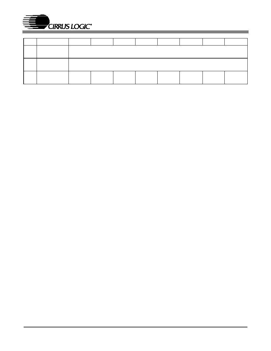
CS4385
36
DS671A1
14h Vol. Control A4
A4_VOL7
A4_VOL6
A4_VOL5
A4_VOL4
A4_VOL3
A4_VOL2
A4_VOL1
A4_VOL0
default
0
0
0
0
0
0
0
0
15h Vol. Control B4
B4_VOL7
B4_VOL6
B4_VOL5
B4_VOL4
B4_VOL3
B4_VOL2
B4_VOL1
B4_VOL0
default
0
0
0
0
0
0
0
0
16h PCM clock mode Reserved
Reserved
MCLKDIV
Reserved
Reserved
Reserved
Reserved
Reserved
default
0
0
0
0
0
0
0
0
Addr
Function
7
6
5
4
3
2
1
0
CS4385
DS671A1
37
5.
REGISTER DESCRIPTION
Note:
All registers are read/write in I
2
C mode and write only in SPI, unless otherwise noted.
5.1
Chip Revision (address 01h)
5.1.1 PART NUMBER ID (PART) [READ ONLY]
00001- CS4385
REVISION ID (REV) [READ ONLY]
000 - Revision A
Function:
This read-only register can be used to identify the model and revision number of the device.
5.2
Mode Control 1 (address 02h)
5.2.1 CONTROL PORT ENABLE (CPEN)
Default = 0
0 - Disabled
1 - Enabled
Function:
This bit defaults to 0, allowing the device to power-up in Stand-Alone mode. The Control port mode
can be accessed by setting this bit to 1. This will allow the operation of the device to be controlled by
the registers and the pin definitions will conform to Control Port Mode. To accomplish a clean power-
up, the user should write this bit within 10 ms following the release of Reset.
7
6
5
4
3
2
1
0
PART4
PART3
PART2
PART1
PART0
REV2
REV1
REV0
0
0
0
0
1
-
-
-
7
6
5
4
3
2
1
0
CPEN
FREEZE
DSD/PCM
DAC4_DIS
DAC3_DIS
DAC2_DIS
DAC1_DIS
PDN
0
0
0
0
0
0
0
1

CS4385
38
DS671A1
5.2.2 FREEZE CONTROLS (FREEZE)
Default = 0
0 - Disabled
1 - Enabled
Function:
This function allows modifications to be made to the registers without the changes taking effect until
the FREEZE is disabled. To make multiple changes in the Control port registers take effect simulta-
neously, enable the FREEZE Bit, make all register changes, then Disable the FREEZE bit.
5.2.3 PCM/DSD SELECTION (DSD/PCM)
Default = 0
0 - PCM
1 - DSD
Function:
This function selects DSD or PCM Mode. The appropriate data and clocks should be present before
changing modes, or else MUTE should be selected.
5.2.4 DAC PAIR DISABLE (DACX_DIS)
Default = 0
0 - Enabled
1 - Disabled
Function:
When enabled the respective DAC channel pairx (AOUTAx and AOUTBx) will remain in a reset state.
It is advised that changes to these bits be made while the power down bit is enabled to eliminate the
possibility of audible artifacts.
5.2.5 POWER DOWN (PDN)
Default = 1
0 - Disabled
1 - Enabled
Function:
The entire device will enter a low-power state when this function is enabled, and the contents of the
control registers are retained in this mode. The power-down bit defaults to `enabled' on power-up and
must be disabled before normal operation in Control Port mode can occur.
CS4385
DS671A1
39
5.3
PCM Control (address 03h)
5.3.1 DIGITAL INTERFACE FORMAT (DIF)
Default = 0000 - Format 0 (Left Justified, up to 24-bit data)
Function:
These bits select the interface format for the serial audio input. The DSD/PCM bit determines whether
PCM or DSD mode is selected.
The required relationship between the Left/Right clock, serial clock and serial data is defined by the Digital
Interface Format and the options are detailed in Figures 9-19.
5.3.2 FUNCTIONAL MODE (FM)
Default = 11
00 - Single-Speed Mode (4 to 50 kHz sample rates)
01 - Double-Speed Mode (50 to 100 kHz sample rates)
10 - Quad-Speed Mode (100 to 200 kHz sample rates)
11 - Auto Speed Mode detect (32 kHz to 200 kHz sample rates)
Function:
Selects the required range of input sample rates or Auto Speed Mode.
7
6
5
4
3
2
1
0
DIF3
DIF2
DIF1
DIF0
Reserved
Reserved
FM1
FM0
0
0
0
0
0
0
1
1
DIF3
DIF2
DIF1
DIF0
DESCRIPTION
Format
FIGURE
0
0
0
0
Left Justified, up to 24-bit data
0
9
0
0
0
1
I
2
S, up to 24-bit data
1
10
0
0
1
0
Right Justified, 16-bit data
2
11
0
0
1
1
Right Justified, 24-bit data
3
12
0
1
0
0
Right Justified, 20-bit data
4
13
0
1
0
1
Right Justified, 18-bit data
5
14
1
0
0
0
One-line Mode 1, 24-bit Data +SDIN4
8
15
1
0
0
1
One-line Mode 2, 20-bit Data +SDIN4
9
16
1
0
1
0
One-line Mode 3, 24-bit 6-channel
10
17
1
0
1
1
One-line Mode 4, 20-bit 6-channel
11
18
1
1
0
0
TDM
12
19
X
X
X
X
All other combinations are Reserved
Table 7. Digital Interface Formats - PCM Mode
CS4385
40
DS671A1
5.4
DSD Control (address 04h)
5.4.1 DSD MODE DIGITAL INTERFACE FORMAT (DSD_DIF)
Default = 000 - Format 0 (64x oversampled DSD data with a 4x MCLK to DSD data rate)
Function:
The relationship between the oversampling ratio of the DSD audio data and the required Master clock to
DSD data rate is defined by the Digital Interface Format pins.
The DSD/PCM bit determines whether PCM or DSD mode is selected.
5.4.2 DIRECT DSD CONVERSION (DIR_DSD)
Function:
When set to 0 (default), DSD input data is sent to the DSD processor for filtering and volume control func-
tions.
When set to 1, DSD input data is sent directly to the switched capacitor DACs for a pure DSD conversion.
In this mode the full scale DSD and PCM levels will not be matched (see Section 2), the dynamic range
performance may be reduced, the volume control is inactive, and the 50 kHz low pass filter is not available
(see section 2 for filter specifications).
5.4.3 STATIC DSD DETECT (STATIC_DSD)
Function:
When set to 1 (default), the DSD processor checks for 28 consecutive zeroes or ones and, if detected,
sends a mute signal to the DACs. The MUTEC pins will eventually go active according to the DAMUTE
register.
When set to 0, this function is disabled.
7
6
5
4
3
2
1
0
DSD_DIF2
DSD_DIF1
DSD_DIF0
DIR_DSD
STATIC_DSD INVALID_DSD DSD_PM_MD DSD_PM_EN
0
0
0
0
1
1
0
0
DIF2
DIF1
DIFO
DESCRIPTION
0
0
0
64x oversampled DSD data with a 4x MCLK to DSD data rate
0
0
1
64x oversampled DSD data with a 6x MCLK to DSD data rate
0
1
0
64x oversampled DSD data with a 8x MCLK to DSD data rate
0
1
1
64x oversampled DSD data with a 12x MCLK to DSD data rate
1
0
0
128x oversampled DSD data with a 2x MCLK to DSD data rate
1
0
1
128x oversampled DSD data with a 3x MCLK to DSD data rate
1
1
0
128x oversampled DSD data with a 4x MCLK to DSD data rate
1
1
1
128x oversampled DSD data with a 6x MCLK to DSD data rate
Table 8. Digital Interface Formats - DSD Mode

CS4385
DS671A1
41
5.4.4 INVALID DSD DETECT (INVALID_DSD)
Function:
When set to 1, the DSD processor checks for greater than 24 out of 28 bits of the same value and, if de-
tected, will attenuate the data sent to the DACs. The MUTEC pins go active according to the DAMUTE
register.
When set to 0 (default), this function is disabled.
5.4.5 DSD PHASE MODULATION MODE SELECT (DSD_PM_MODE)
Function:
When set to 0 (default), the 128Fs (BCKA) clock should be input to DSD_SCLK for phase modulation
mode. (See Figure 22 on page 26)
When set to 1, the 64Fs (BCKD) clock should be input to DSD_SCLK for phase modulation mode.
5.4.6 DSD PHASE MODULATION MODE ENABLE (DSD_PM_EN)
Function:
When set to 1, DSD phase modulation input mode is enabled and the DSD_PM_MODE bit should be set
accordingly.
When set to 0 (default), this function is disabled (DSD normal mode).
5.5
Filter Control (address 05h)
5.5.1 INTERPOLATION FILTER SELECT (FILT_SEL)
Function:
When set to 0 (default), the Interpolation Filter has a fast roll off.
When set to 1, the Interpolation Filter has a slow roll off.
The specifications for each filter can be found in the Analog characteristics table, and response plots can
be found in figures 28 to 51 found on the page 26.
7
6
5
4
3
2
1
0
Reserved
Reserved
Reserved
Reserved
Reserved
Reserved
Reserved
FILT_SEL
0
0
0
0
0
0
0
0
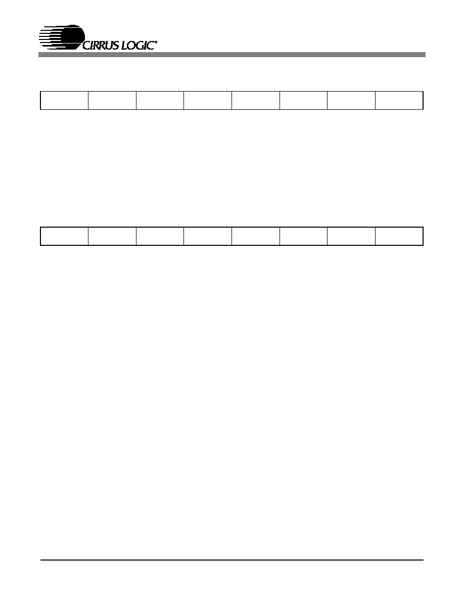
CS4385
42
DS671A1
5.6
Invert Control (address 06h)
5.6.1 INVERT SIGNAL POLARITY (INV_XX)
Function:
When set to 1, this bit inverts the signal polarity of channel xx.
When set to 0 (default), this function is disabled.
5.7
Group Control (address 07h)
5.7.1 MUTEC PIN CONTROL(MUTEC)
Default = 0
0 - Two Mute control signals
1 - Single mute control signal on MUTEC1
Function:
Selects how the internal mute signals are routed to the MUTEC1 and MUTEC234 pins. When set to
`0', a logical AND of DAC pair 1 mute control signals are output on MUTEC1 and a logical AND of the
mute control signals of DAC pairs 2, 3, and 4 are output on MUTEC234. When set to `1', a logical AND
of all DAC pair mute control signals is output on the MUTEC1 pin, MUTEC234 will remain static. For
more information on the use of the mute control function see the MUTEC1 and MUTEC234 pins in
section 3.11.
5.7.2 CHANNEL A VOLUME = CHANNEL B VOLUME (PX_A=B)
Default = 0
0 - Disabled
1 - Enabled
Function:
The AOUTAx and AOUTBx volume levels are independently controlled by the A and the B Channel Vol-
ume Control Bytes when this function is disabled. The volume on both AOUTAx and AOUTBx are deter-
mined by the A Channel Attenuation and Volume Control Bytes (per A-B pair), and the B Channel Bytes
are ignored when this function is enabled.
5.7.3 SINGLE VOLUME CONTROL (SNGLVOL)
Default = 0
0 - Disabled
1 - Enabled
7
6
5
4
3
2
1
0
INV_B4
INV_A4
INV_B3
INV_A3
INV_B2
INV_A2
INV_B1
INV_A1
0
0
0
0
0
0
0
0
7
6
5
4
3
2
1
0
Reserved
MUTEC
Reserved
P1_A=B
P2_A=B
P3_A=B
P4_A=B
SNGLVOL
0
0
1
0
0
1
0
0
CS4385
DS671A1
43
Function:
The individual channel volume levels are independently controlled by their respective Volume Control
Bytes when this function is disabled. The volume on all channels is determined by the A1 Channel
Volume Control Byte, and the other Volume Control Bytes are ignored when this function is enabled.
5.8
Ramp and Mute (address 08h)
5.8.1 SOFT RAMP AND ZERO CROSS CONTROL (SZC)
Default = 10
00 - Immediate Change
01 - Zero Cross
10 - Soft Ramp
11 - Soft Ramp on Zero Crossings
Function:
Immediate Change
When Immediate Change is selected all level changes will take effect immediately in one step.
Zero Cross
Zero Cross Enable dictates that signal level changes, either by attenuation changes or muting, will
occur on a signal zero crossing to minimize audible artifacts. The requested level change will occur
after a timeout period between 512 and 1024 sample periods (10.7 ms to 21.3 ms at 48 kHz sample
rate) if the signal does not encounter a zero crossing. The zero cross function is independently mon-
itored and implemented for each channel.
Soft Ramp
Soft Ramp allows level changes, both muting and attenuation, to be implemented by incrementally
ramping, in 1/8 dB steps, from the current level to the new level at a rate of 1 dB per 8 left/right clock
periods.
Soft Ramp on Zero Crossing
Soft Ramp and Zero Cross Enable dictates that signal level changes, either by attenuation changes
or muting, will occur in 1/8 dB steps and be implemented on a signal zero crossing. The 1/8 dB level
change will occur after a timeout period between 512 and 1024 sample periods (10.7 ms to 21.3 ms
at 48 kHz sample rate) if the signal does not encounter a zero crossing. The zero cross function is
independently monitored and implemented for each channel.
5.8.2 SOFT VOLUME RAMP-UP AFTER ERROR (RMP_UP)
Function:
7
6
5
4
3
2
1
0
SZC1
SZC0
RMP_UP
RMP_DN
PAMUTE
DAMUTE
MUTE_P1
MUTE_P0
1
0
0
0
0
0
0
0

CS4385
44
DS671A1
When set to 1 (default), an un-mute will be performed after executing a filter mode change, after a
LRCK/MCLK ratio change or error, and after changing the Functional Mode. This un-mute is effected, sim-
ilar to attenuation changes, by the Soft and Zero Cross bits in the Volume and Mixing Control register.
When set to 0, an immediate un-mute is performed in these instances.
Note: For best results, it is recommended that this feature be used in conjunction with the RMP_DN bit.
5.8.3 SOFT RAMP-DOWN BEFORE FILTER MODE CHANGE (RMP_DN)
Function:
When set to 1 (default), a mute will be performed prior to executing a filter mode change. This mute is
effected, similar to attenuation changes, by the Soft and Zero Cross bits in the Volume and Mixing Control
register.
When set to 0, an immediate mute is performed prior to executing a filter mode change.
Note: For best results, it is recommended that this feature be used in conjunction with the RMP_UP bit.
5.8.4 PCM AUTO-MUTE (PAMUTE)
Function:
When set to 1 (default) the Digital-to-Analog converter output will mute following the reception of 8192
consecutive audio samples of static 0 or -1. A single sample of non-static data will release the mute. De-
tection and muting is done independently for each channel. The quiescent voltage on the output will be
retained and the Mute Control pin will go active during the mute period.
When set to 0 this function is disabled.
5.8.5 DSD AUTO-MUTE (DAMUTE)
Function:
When set to 1 (default) the Digital-to-Analog converter output will mute following the reception of 256 re-
peated 8-bit DSD mute patterns (as defined in the SACD specification).
A single bit not fitting the repeated mute pattern (mentioned above) will release the mute. Detection and
muting is done independently for each channel. The quiescent voltage on the output will be retained and
the Mute Control pin will go active during the mute period.
CS4385
DS671A1
45
5.8.6 MUTE POLARITY AND DETECT (MUTEP1:0)
Default = 00
00 - Auto polarity detect, selected from MUTEC1 pin
01 - Reserved
10 - Active low mute polarity
11 - Active high mute polarity
Function:
Auto mute polarity detect (00)
See section 3.11 on page 29 for description.
Active low mute polarity (10)
When RST is low the outputs are high impedance and will need to be biased active. Once reset has been
released and after this bit is set, the MUTEC output pins will be active low polarity.
Active high mute polarity (11)
At reset time the outputs are high impedance and will need to be biased active. Once reset has been
released and after this bit is set, the MUTEC output pins will be active high polarity.
5.9
Mute Control (address 09h)
5.9.1 MUTE (MUTE_XX)
Default = 0
0 - Disabled
1 - Enabled
Function:
The Digital-to-Analog converter output will mute when enabled. The quiescent voltage on the output will
be retained. The muting function is affected, similarly to attenuation changes, by the Soft and Zero Cross
bits. The MUTE pins will go active during the mute period according to the MUTEC bit.
7
6
5
4
3
2
1
0
MUTE_B4
MUTE_A4
MUTE_B3
MUTE_A3
MUTE_B2
MUTE_A2
MUTE_B1
MUTE_A1
0
0
0
0
0
0
0
0
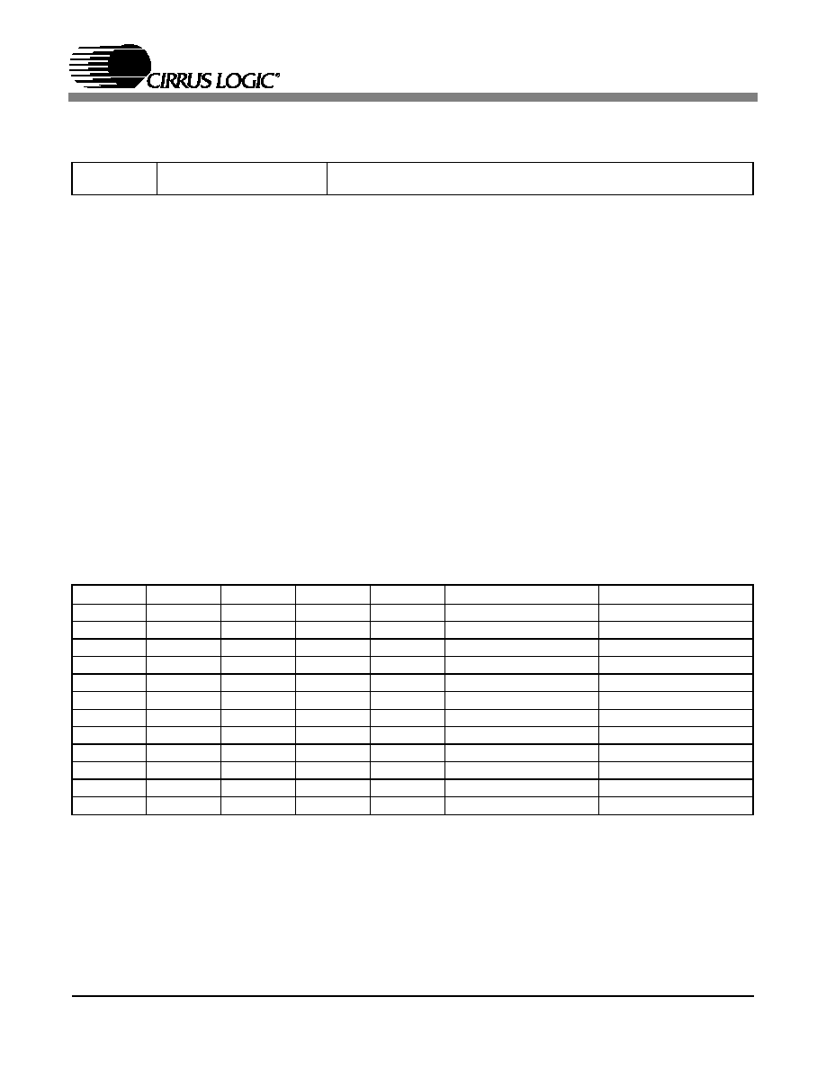
CS4385
46
DS671A1
5.10 Mixing Control (address 0Ah, 0Dh, 10h, 13h)
5.10.1 DE-EMPHASIS CONTROL (PX_DEM1:0)
Default = 00
00 - Disabled
01 - 44.1 kHz
10 - 48 kHz
11 - 32 kHz
Function:
Selects the appropriate digital filter to maintain the standard 15
�
s/50
�
s digital de-emphasis filter re-
sponse at 32, 44.1 or 48 kHz sample rates. (see Figure 20)
De-emphasis is only available in Single Speed Mode.
5.10.2 ATAPI CHANNEL MIXING AND MUTING (ATAPI)
Default = 01001 - AOUTAx=aL, AOUTBx=bR (Stereo)
Function:
The implements the channel mixing functions of the ATAPI CD-ROM specification. The ATAPI functions
are applied per A-B pair. Refer to Table 14 and Figure 21 for additional information.
7
6
5
4
3
2
1
0
Reserved
Px_DEM1
Px_DEM0
PxATAPI4
PxATAPI3
PxATAPI2
PxATAPI1
PxATAPI0
0
0
1
0
1
0
0
1
ATAPI4
ATAPI3
ATAPI2
ATAPI1
ATAPI0
AOUTAx
AOUTBx
0
0
0
0
0
MUTE
MUTE
0
0
0
0
1
MUTE
bR
0
0
0
1
0
MUTE
bL
0
0
0
1
1
MUTE
b[(L+R)/2]
0
0
1
0
0
aR
MUTE
0
0
1
0
1
aR
bR
0
0
1
1
0
aR
bL
0
0
1
1
1
aR
b[(L+R)/2]
0
1
0
0
0
aL
MUTE
0
1
0
0
1
aL
bR
0
1
0
1
0
aL
bL
0
1
0
1
1
aL
b[(L+R)/2]
Table 9. ATAPI Decode
CS4385
DS671A1
47
0
1
1
0
0
a[(L+R)/2]
MUTE
0
1
1
0
1
a[(L+R)/2]
bR
0
1
1
1
0
a[(L+R)/2]
bL
0
1
1
1
1
a[(L+R)/2]
b[(L+R)/2]
1
0
0
0
0
MUTE
MUTE
1
0
0
0
1
MUTE
bR
1
0
0
1
0
MUTE
bL
1
0
0
1
1
MUTE
[(bL+aR)/2]
1
0
1
0
0
aR
MUTE
1
0
1
0
1
aR
bR
1
0
1
1
0
aR
bL
1
0
1
1
1
aR
[(aL+bR)/2]
1
1
0
0
0
aL
MUTE
1
1
0
0
1
aL
bR
1
1
0
1
0
aL
bL
1
1
0
1
1
aL
[(aL+bR)/2]
1
1
1
0
0
[(aL+bR)/2]
MUTE
1
1
1
0
1
[(aL+bR)/2]
bR
1
1
1
1
0
[(bL+aR)/2]
bL
1
1
1
1
1
[(aL+bR)/2]
[(aL+bR)/2]
ATAPI4
ATAPI3
ATAPI2
ATAPI1
ATAPI0
AOUTAx
AOUTBx
Table 9. ATAPI Decode
CS4385
48
DS671A1
5.11 Volume Control (address 0Bh, 0Ch, 0Eh, 0Fh, 11h, 12h, 14h, 15h)
These eight registers provide individual volume and mute control for each of the eight channels.
The values for "xx" in the bit fields above are as follows:
Register address 0Bh - xx = A1
Register address 0Ch - xx = B1
Register address 0Eh - xx = A2
Register address 0Fh - xx = B2
Register address 11h - xx = A3
Register address 12h - xx = B3
Register address 14h - xx = A4
Register address 15h - xx = B4
5.11.1 DIGITAL VOLUME CONTROL (XX_VOL7:0)
Default = 00h (0 dB)
Function:
The Digital Volume Control registers allow independent control of the signal levels in 1/2 dB increments
from 0 to -127.5 dB. Volume settings are decoded as shown in Table 15. The volume changes are imple-
mented as dictated by the Soft and Zero Cross bits in the Power and Muting Control register. Note that
the values in the volume setting column in Table 15 are approximate. The actual attenuation is determined
by taking the decimal value of the volume register and multiplying by 6.02/12.
5.12 PCM Clock Mode (address 16h)
5.12.1 MASTER CLOCK DIVIDE BY 2 ENABLE (MCLKDIV)
Function:
When set to 1, the MCLKDIV bit enables a circuit which divides the externally applied MCLK signal by 2
prior to all other internal circuitry.
When set to 0 (default), MCLK is unchanged.
7
6
5
4
3
2
1
0
xx_VOL7
xx_VOL6
xx_VOL5
xx_VOL4
xx_VOL3
xx_VOL2
xx_VOL1
xx_VOL0
0
0
0
0
0
0
0
0
Table 10. Example Digital Volume Settings
Binary Code
Decimal Value
Volume Setting
00000000
0
0 dB
00000001
1
-0.5 dB
00000110
6
-3.0 dB
11111111
255
-127.5 dB
7
6
5
4
3
2
1
0
Reserved
Reserved
MCLKDIV
Reserved
Reserved
Reserved
Reserved
Reserved
0
0
0
0
0
0
0
0

CS4385
DS671A1
49
6. PARAMETER DEFINITIONS
Total Harmonic Distortion + Noise (THD+N)
The ratio of the rms value of the signal to the rms sum of all other spectral components over the specified
bandwidth (typically 10 Hz to 20 kHz), including distortion components. Expressed in decibels.
Dynamic Range
The ratio of the full scale rms value of the signal to the rms sum of all other spectral components over the
specified bandwidth. Dynamic range is a signal-to-noise measurement over the specified bandwidth
made with a -60 dBFS signal. 60 dB is then added to the resulting measurement to refer the measurement
to full scale. This technique ensures that the distortion components are below the noise level and do not
affect the measurement. This measurement technique has been accepted by the Audio Engineering So-
ciety, AES17-1991, and the Electronic Industries Association of Japan, EIAJ CP-307.
Interchannel Isolation
A measure of crosstalk between the left and right channels. Measured for each channel at the converter's
output with all zeros to the input under test and a full-scale signal applied to the other channel. Units in
decibels.
Interchannel Gain Mismatch
The gain difference between left and right channels. Units in decibels.
Gain Error
The deviation from the nominal full scale analog output for a full scale digital input.
Gain Drift
The change in gain value with temperature. Units in ppm/�C.
7. REFERENCES
1. "How to Achieve Optimum Performance from Delta-Sigma A/D & D/A Converters" by Steven Harris.
Paper presented at the 93rd Convention of the Audio Engineering Society, October 1992.
2. CDB4385 Evaluation Board Datasheet
3. "Design Notes for a 2-Pole Filter with Differential Input" by Steven Green. Cirrus Logic Application Note
AN48
4. "The I
2
C-Bus Specification: Version 2.0" Philips Semiconductors, December 1998.
http://www.semiconductors.philips.com
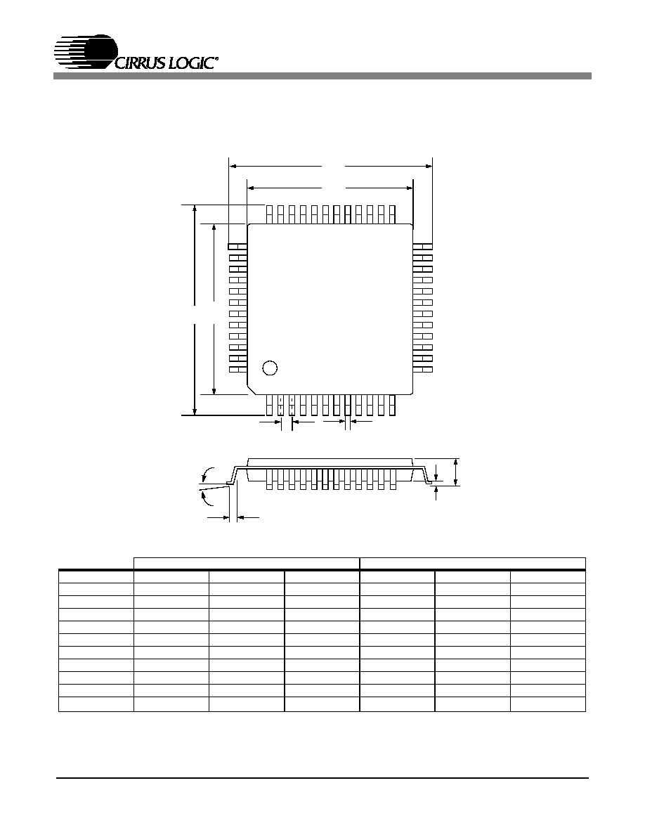
CS4385
50
DS671A1
8. PACKAGE DIMENSIONS
INCHES
MILLIMETERS
DIM
MIN
NOM
MAX
MIN
NOM
MAX
A
---
0.055
0.063
---
1.40
1.60
A1
0.002
0.004
0.006
0.05
0.10
0.15
B
0.007
0.009
0.011
0.17
0.22
0.27
D
0.343
0.354
0.366
8.70
9.0 BSC
9.30
D1
0.272
0.28
0.280
6.90
7.0 BSC
7.10
E
0.343
0.354
0.366
8.70
9.0 BSC
9.30
E1
0.272
0.28
0.280
6.90
7.0 BSC
7.10
e*
0.016
0.020
0.024
0.40
0.50 BSC
0.60
L
0.018
0.24
0.030
0.45
0.60
0.75
0.000�
4�
7.000�
0.00�
4�
7.00�
* Nominal pin pitch is 0.50 mm
Controlling dimension is mm.
JEDEC Designation: MS022
48L LQFP PACKAGE DRAWING
E1
E
D1
D
1
e
L
B
A1
A
CS4385
DS671A1
51
9. APPENDIX
0.4
0.5
0.6
0.7
0.8
0.9
1
-120
-100
-80
-60
-40
-20
0
Frequency(normalized to Fs)
Amplitude (dB)
0.4
0.42
0.44
0.46
0.48
0.5
0.52
0.54
0.56
0.58
0.6
-120
-100
-80
-60
-40
-20
0
Frequency(normalized to Fs)
Amplitude (dB)
Figure 28. Single Speed (fast) Stopband Rejection
Figure 29. Single Speed (fast) Transition Band
0.45
0.46
0.47
0.48
0.49
0.5
0.51
0.52
0.53
0.54
0.55
-10
-9
-8
-7
-6
-5
-4
-3
-2
-1
0
Frequency(normalized to Fs)
Amplitude (dB)
0
0.05
0.1
0.15
0.2
0.25
0.3
0.35
0.4
0.45
0.5
-0.02
-0.015
-0.01
-0.005
0
0.005
0.01
0.015
0.02
Frequency(normalized to Fs)
Amplitude (dB)
Figure 30. Single Speed (fast) Transition Band (detail)
Figure 31. Single Speed (fast) Passband Ripple
0.4
0.5
0.6
0.7
0.8
0.9
1
-120
-100
-80
-60
-40
-20
0
Frequency(normalized to Fs)
Amplitude (dB)
0.4
0.42
0.44
0.46
0.48
0.5
0.52
0.54
0.56
0.58
0.6
-120
-100
-80
-60
-40
-20
0
Frequency(normalized to Fs)
Amplitude (dB)
Figure 32. Single Speed (slow) Stopband Rejection
Figure 33. Single Speed (slow) Transition Band
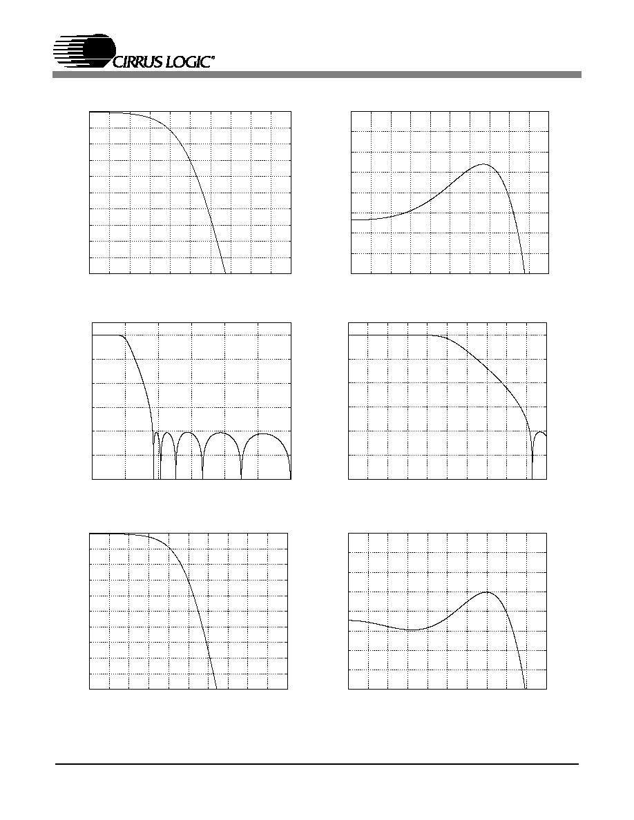
CS4385
52
DS671A1
0
0.05
0.1
0.15
0.2
0.25
0.3
0.35
0.4
0.45
0.5
-0.02
-0.015
-0.01
-0.005
0
0.005
0.01
0.015
0.02
Frequency(normalized to Fs)
Amplitude (dB)
0.45
0.46
0.47
0.48
0.49
0.5
0.51
0.52
0.53
0.54
0.55
-10
-9
-8
-7
-6
-5
-4
-3
-2
-1
0
Frequency(normalized to Fs)
Amplitude (dB)
Figure 34. Single Speed (slow) Transition Band (detail)
Figure 35. Single Speed (slow) Passband Ripple
0.4
0.5
0.6
0.7
0.8
0.9
1
120
100
80
60
40
20
0
Frequency(normalized to Fs)
Amplitude (dB)
0.4
0.42
0.44
0.46
0.48
0.5
0.52
0.54
0.56
0.58
0.6
120
100
80
60
40
20
0
Frequency(normalized to Fs)
Amplitude (dB)
Figure 36. Double Speed (fast) Stopband Rejection
Figure 37. Double Speed (fast) Transition Band
0.45
0.46
0.47
0.48
0.49
0.5
0.51
0.52
0.53
0.54
0.55
10
9
8
7
6
5
4
3
2
1
0
Frequency(normalized to Fs)
Amplitude (dB)
0
0.05
0.1
0.15
0.2
0.25
0.3
0.35
0.4
0.45
0.5
0.02
0.015
0.01
0.005
0
0.005
0.01
0.015
0.02
Frequency(normalized to Fs)
Amplitude (dB)
Figure 38. Double Speed (fast) Transition Band (detail)
Figure 39. Double Speed (fast) Passband Ripple

CS4385
DS671A1
53
0.2
0.3
0.4
0.5
0.6
0.7
0.8
0.9
1
120
100
80
60
40
20
0
Frequency(normalized to Fs)
Amplitude (dB)
0.2
0.3
0.4
0.5
0.6
0.7
0.8
120
100
80
60
40
20
0
Frequency(normalized to Fs)
Amplitude (dB)
Figure 40. Double Speed (slow) Stopband Rejection
Figure 41. Double Speed (slow) Transition Band
0.45
0.46
0.47
0.48
0.49
0.5
0.51
0.52
0.53
0.54
0.55
10
9
8
7
6
5
4
3
2
1
0
Frequency(normalized to Fs)
Amplitude (dB)
0
0.05
0.1
0.15
0.2
0.25
0.3
0.35
0.02
0.015
0.01
0.005
0
0.005
0.01
0.015
0.02
Frequency(normalized to Fs)
Amplitude (dB)
Figure 42. Double Speed (slow) Transition Band (detail)
Figure 43. Double Speed (slow) Passband Ripple
0.2
0.3
0.4
0.5
0.6
0.7
0.8
0.9
1
120
100
80
60
40
20
0
Frequency(normalized to Fs)
Amplitude (dB)
0.2
0.3
0.4
0.5
0.6
0.7
0.8
120
100
80
60
40
20
0
Frequency(normalized to Fs)
Amplitude (dB)
Figure 44. Quad Speed (fast) Stopband Rejection
Figure 45. Quad Speed (fast) Transition Band
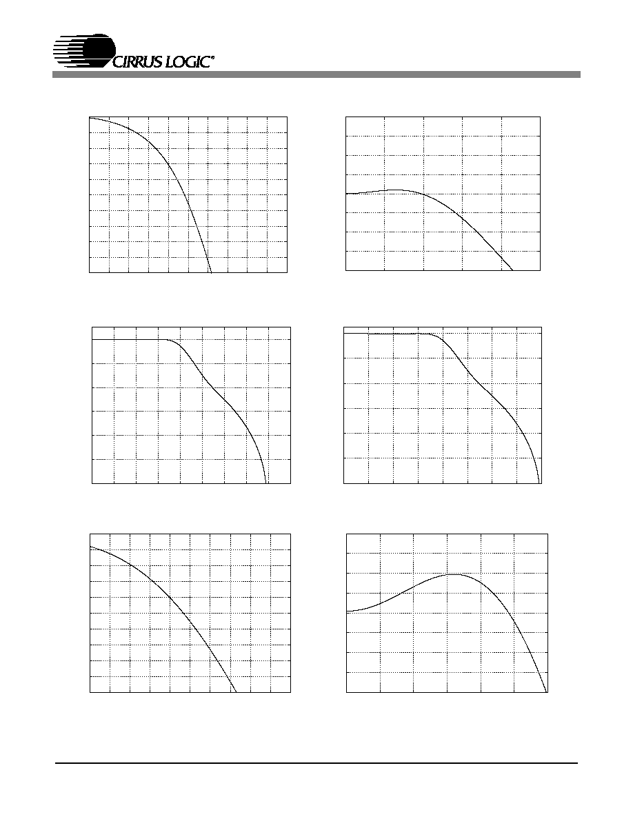
CS4385
54
DS671A1
0.45
0.46
0.47
0.48
0.49
0.5
0.51
0.52
0.53
0.54
0.55
10
9
8
7
6
5
4
3
2
1
0
Frequency(normalized to Fs)
Amplitude (dB)
0
0.05
0.1
0.15
0.2
0.25
0.2
0.15
0.1
0.05
0
0.05
0.1
0.15
0.2
Frequency(normalized to Fs)
Amplitude (dB)
Figure 46. Quad Speed (fast) Transition Band (detail)
Figure 47. Quad Speed (fast) Passband Ripple
0.1
0.2
0.3
0.4
0.5
0.6
0.7
0.8
0.9
1
120
100
80
60
40
20
0
Frequency(normalized to Fs)
Amplitude (dB)
0.1
0.2
0.3
0.4
0.5
0.6
0.7
0.8
0.9
120
100
80
60
40
20
0
Frequency(normalized to Fs)
Amplitude (dB)
Figure 48. Quad Speed (slow) Stopband Rejection
Figure 49. Quad Speed (slow) Transition Band
0.45
0.46
0.47
0.48
0.49
0.5
0.51
0.52
0.53
0.54
0.55
10
9
8
7
6
5
4
3
2
1
0
Frequency(normalized to Fs)
Amplitude (dB)
0
0.02
0.04
0.06
0.08
0.1
0.12
0.02
0.015
0.01
0.005
0
0.005
0.01
0.015
0.02
Frequency(normalized to Fs)
Amplitude (dB)
Figure 50. Quad Speed (slow) Transition Band (detail)
Figure 51. Quad Speed (slow) Passband Ripple
CS4385
DS671A1
55
Table 11. Revision History
Contacting Cirrus Logic Support
For a complete listing of Direct Sales, Distributor, and Sales Representative contacts, visit the Cirrus Logic web site at:
http://www.cirrus.com/corporate/contacts
IMPORTANT NOTICE
"Advance" product information describes products that are in development and subject to development changes.Cirrus Logic, Inc. and its subsidiaries ("Cirrus")
believe that the information contained in this document is accurate and reliable. However, the information is subject to change without notice and is provided "AS
IS" without warranty of any kind (express or implied). Customers are advised to obtain the latest version of relevant information to verify, before placing orders, that
information being relied on is current and complete. All products are sold subject to the terms and conditions of sale supplied at the time of order acknowledgment,
including those pertaining to warranty, patent infringement, and limitation of liability. No responsibility is assumed by Cirrus for the use of this information, including
use of this information as the basis for manufacture or sale of any items, or for infringement of patents or other rights of third parties. This document is the property
of Cirrus and by furnishing this information, Cirrus grants no license, express or implied under any patents, mask work rights, copyrights, trademarks, trade secrets
or other intellectual property rights. Cirrus owns the copyrights associated with the information contained herein and gives consent for copies to be made of the
information only for use within your organization with respect to Cirrus integrated circuits or other products of Cirrus. This consent does not extend to other copying
such as copying for general distribution, advertising or promotional purposes, or for creating any work for resale.
CERTAIN APPLICATIONS USING SEMICONDUCTOR PRODUCTS MAY INVOLVE POTENTIAL RISKS OF DEATH, PERSONAL INJURY, OR SEVERE PROP-
ERTY OR ENVIRONMENTAL DAMAGE ("CRITICAL APPLICATIONS"). CIRRUS PRODUCTS ARE NOT DESIGNED, AUTHORIZED OR WARRANTED FOR
USE IN AIRCRAFT SYSTEMS, MILITARY APPLICATIONS, PRODUCTS SURGICALLY IMPLANTED INTO THE BODY, LIFE SUPPORT PRODUCTS OR OTHER
CRITICAL APPLICATIONS (INCLUDING MEDICAL DEVICES, AIRCRAFT SYSTEMS OR COMPONENTS AND PERSONAL OR AUTOMOTIVE SAFETY OR SE-
CURITY DEVICES). INCLUSION OF CIRRUS PRODUCTS IN SUCH APPLICATIONS IS UNDERSTOOD TO BE FULLY AT THE CUSTOMER'S RISK AND CIR-
RUS DISCLAIMS AND MAKES NO WARRANTY, EXPRESS, STATUTORY OR IMPLIED, INCLUDING THE IMPLIED WARRANTIES OF MERCHANTABILITY
AND FITNESS FOR PARTICULAR PURPOSE, WITH REGARD TO ANY CIRRUS PRODUCT THAT IS USED IN SUCH A MANNER. IF THE CUSTOMER OR
CUSTOMER'S CUSTOMER USES OR PERMITS THE USE OF CIRRUS PRODUCTS IN CRITICAL APPLICATIONS, CUSTOMER AGREES, BY SUCH USE, TO
FULLY INDEMNIFY CIRRUS, ITS OFFICERS, DIRECTORS, EMPLOYEES, DISTRIBUTORS AND OTHER AGENTS FROM ANY AND ALL LIABILITY, INCLUD-
ING ATTORNEYS' FEES AND COSTS, THAT MAY RESULT FROM OR ARISE IN CONNECTION WITH THESE USES.
Purchase of I
2
C components of Cirrus Logic, Inc., or one of its sublicensed Associated Companies conveys a license under the Phillips I
2
C Patent Rights to use
those components in a standard I
2
C system.
Cirrus Logic, Cirrus, and the Cirrus Logic logo designs are trademarks of Cirrus Logic, Inc. All other brand and product names in this document may be trademarks
or service marks of their respective owners.
Release
Date
Changes
A1
OCT 2004
Initial Release

CS4385
56
DS671A1