| –≠–ª–µ–∫—Ç—Ä–æ–Ω–Ω—ã–π –∫–æ–º–ø–æ–Ω–µ–Ω—Ç: CDB4396 | –°–∫–∞—á–∞—Ç—å:  PDF PDF  ZIP ZIP |
Advance Product Information
This document contains information for a new product.
Cirrus Logic reserves the right to modify this product without notice.
1
Copyright
©
Cirrus Logic, Inc. 1999
(All Rights Reserved)
P.O. Box 17847, Austin, Texas 78760
(512) 445 7222 FAX: (512) 445 7581
http://www.cirrus.com
CS4396
24-Bit, 192 kHz D/A Converter for Digital Audio
Features
l
24 Bit Conversion
l
Up to 192 kHz Sample Rates
l
120 dB Dynamic Range
l
-100 dB THD+N
l
Advanced Dynamic-Element Matching
l
Low Clock Jitter Sensitivity
l
Digital De-emphasis for 32 kHz, 44.1 kHz and
48 kHz
l
External Reference Input
Description
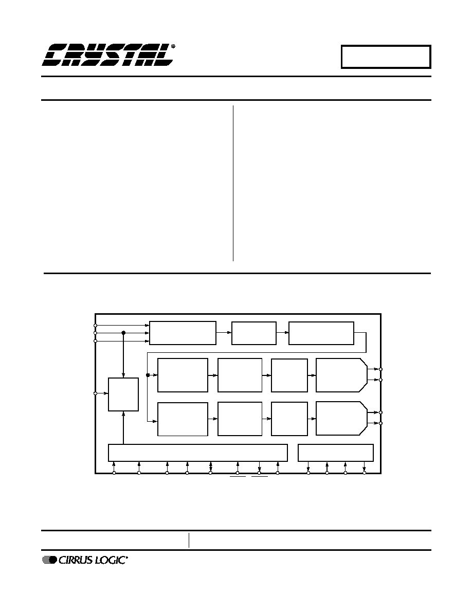
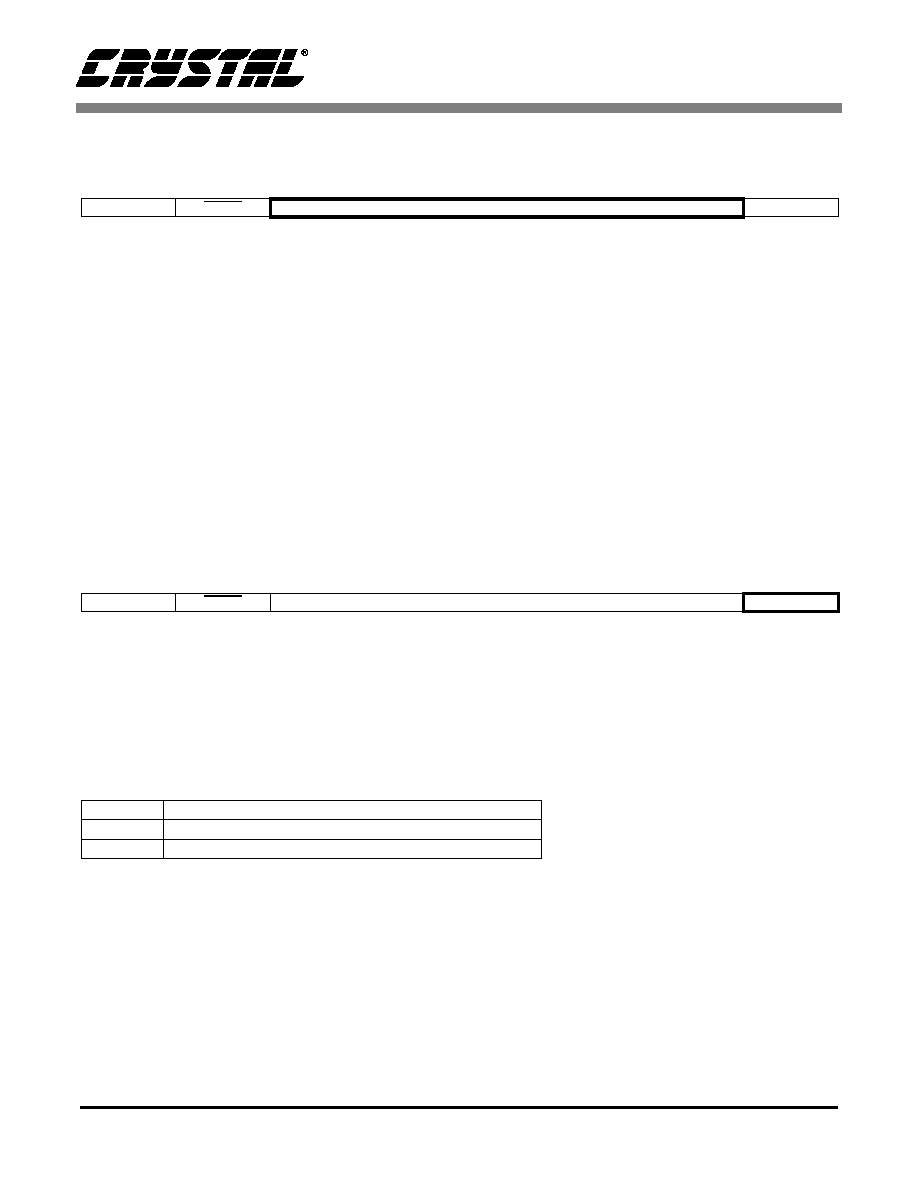
The CS4396 is a complete high performance 24-bit
48/96/192 kHz stereo digital-to-analog conversion sys-
tem. The device includes a digital interpolation filter
followed by a oversampled multi-bit delta-sigma modula-
tor which drives dynamic-element-matching (DEM)
selection logic. The output from the DEM block controls
the input to a multi-element switched capacitor DAC/low-
pass filter, with fully-differential outputs. This multi-bit ar-
chitecture features significantly lower out-of-band noise
and jitter sensitivity than traditional 1-bit designs, and the
advanced DEM guarantees low noise and distortion at
all signal levels.
ORDERING INFORMATION
CS4396-KS
-10∞ to 70∞ C 28-pin Plastic SOIC
CDB4397
Evaluation Board
I
SCLK
MCLK
M4
LRCK
SDATA
AOUTL+
AOUTR+
SERIAL INTERFACE
AND FORMAT SELECT
INTERPOLATION
SOFT MUTE
MODULATOR
DYNAMIC
DE-EMPHASIS
SWITCHED
AOUTL-
AOUTR-
FILT+
FILTER
INTERPOLATION
FILTER
FILTER
MULTI-BIT
MODULATOR
MULTI-BIT
ELEMENT
MATCHING
LOGIC
DYNAMIC
ELEMENT
MATCHING
LOGIC
CAPACITOR-DAC
AND FILTER
SWITCHED
CAPACITOR-DAC
AND FILTER
VREF
CMOUT
FILT-
VOLTAGE REFERENCE
HARDWARE MODE CONTROL
CLOCK
DIVIDER
(CONTROL PORT)
(AD0/CS)
M3
M2
(AD1/CDIN) (SCL/CCLK)
M1
M0
(SDA/CDOUT)
RESET
MUTEC MUTE
JUL `99
DS288PP1

CS4396
2
DS288PP1
TABLE OF CONTENTS
1.0 CHARACTERISTICS/SPECIFICATIONS ..................................................................... 4
ANALOG CHARACTERISTICS................................................................................... 4
Dynamic Performance - Single Speed Mode - Fs equal to 48 kHz ...................... 4
Dynamic Performance - Double Speed Mode - Fs equal to 96 kHz .................... 4
Dynamic Performance - Quad-Speed Mode - Fs equal to 192 kHz ..................... 4
ANALOG CHARACTERISTICS................................................................................... 5
Power Supplies .................................................................................................... 5
Analog Output ...................................................................................................... 5
Combined Digital and On-chip Analog Filter Response - Single Speed Mode .... 6
Combined Digital and On-chip Analog Filter Response - Double Speed Mode ... 6
Combined Digital and On-chip Analog Filter Response - Quad-Speed Mode ..... 6
DIGITAL CHARACTERISTICS.................................................................................... 7
ABSOLUTE MAXIMUM RATINGS .............................................................................. 7
RECOMMENDED OPERATING CONDITIONS .......................................................... 7
SWITCHING CHARACTERISTICS ............................................................................. 8
SWITCHING CHARACTERISTICS - CONTROL PORT ............................................. 9
I
2
C
Æ
Mode ............................................................................................................ 9
SPI Mode ........................................................................................................... 10
2.0 TYPICAL CONNECTION DIAGRAM .......................................................................... 11
3.0 REGISTER DESCRIPTION ........................................................................................ 12
3.1 Differential DC offset calibration ........................................................................ 12
3.2 Soft Mute ........................................................................................................... 12
3.3 Mode Select ....................................................................................................... 13
3.4 Power DowN ...................................................................................................... 13
4.0 PIN DESCRIPTION ..................................................................................................... 14
5.0 APPLICATIONS .......................................................................................................... 19
5.1 Recommended Power-up Sequence ................................................................. 19
6.0 CONTROL PORT INTERFACE .................................................................................. 20
6.1 SPI Mode ........................................................................................................... 20
6.2 I
2
C Mode ........................................................................................................... 20
6.2 Memory Address Pointer (MAP) ........................................................................ 20
7.0 PARAMETER DEFINITIONS ...................................................................................... 26
8.0 REFERENCES ............................................................................................................ 26
9.0 PACKAGE DIMENSIONS ........................................................................................... 27
Contacting Cirrus Logic Support
For a complete listing of Direct Sales, Distributor, and Sales Representative contacts, visit the Cirrus Logic web site at:
http://www.cirrus.com/corporate/contacts/
"The I
2
C-Bus Specification: Version 2.0" Philips Semiconductors, December 1998.
http://www.semiconductors.philips.com
Preliminary product information describes products which are in production, but for which full characterization data is not yet available. Advance product infor-
mation describes products which are in development and subject to development changes. Cirrus Logic, Inc. has made best efforts to ensure that the information
contained in this document is accurate and reliable. However, the information is subject to change without notice and is provided "AS IS" without warranty of
any kind (express or implied). No responsibility is assumed by Cirrus Logic, Inc. for the use of this information, nor for infringements of patents or other rights
of third parties. This document is the property of Cirrus Logic, Inc. and implies no license under patents, copyrights, trademarks, or trade secrets. No part of
this publication may be copied, reproduced, stored in a retrieval system, or transmitted, in any form or by any means (electronic, mechanical, photographic, or
otherwise) without the prior written consent of Cirrus Logic, Inc. Items from any Cirrus Logic website or disk may be printed for use by the user. However, no
part of the printout or electronic files may be copied, reproduced, stored in a retrieval system, or transmitted, in any form or by any means (electronic, mechanical,
photographic, or otherwise) without the prior written consent of Cirrus Logic, Inc.Furthermore, no part of this publication may be used as a basis for manufacture
or sale of any items without the prior written consent of Cirrus Logic, Inc. The names of products of Cirrus Logic, Inc. or other vendors and suppliers appearing
in this document may be trademarks or service marks of their respective owners which may be registered in some jurisdictions. A list of Cirrus Logic, Inc. trade-
marks and service marks can be found at http://www.cirrus.com.

CS4396
DS288PP1
3
TABLE OF FIGURES
Figure 1. Serial Audio Input Timing ........................................................................... 8
Figure 2. I
2
C Control Port Timing .............................................................................. 9
Figure 3. SPI Control Port Timing ........................................................................... 10
Figure 4. Typical Connection Diagram - Hardware Mode (Control Port Mode) ....... 11
Figure 5. Control Port Timing, I
2
C Mode ................................................................. 21
Figure 6. Control Port Timing, SPI mode ................................................................ 21
Figure 7. Single-speed Transition Band .................................................................. 23
Figure 8. Single-speed Stopband Rejection ............................................................ 23
Figure 9. Single-speed Transition Band .................................................................. 23
Figure 10.Single-speed Frequency Response ......................................................... 23
Figure 11.Double-speed Stopband .......................................................................... 23
Figure 12.Double-speed Transition Band ................................................................. 23
Figure 13.Double-speed Transition Band ................................................................. 23
Figure 14.Double-speed Frequency Response ........................................................ 23
Figure 15.Quad-speed Stopband Rejection ............................................................. 24
Figure 16.Quad-speed Transition Band ................................................................... 24
Figure 17.Quad-speed Transition Band ................................................................... 24
Figure 18.Quad-speed Frequency Response .......................................................... 24
Figure 19.De-Emphasis Curve ................................................................................. 24
Figure 20. Format 0, Left Justified ............................................................................ 25
Figure 21. Format 1, I
2
S .......................................................................................... 25
Figure 22. Format 2, Right Justified, 16-Bit Data ..................................................... 25
Figure 23.Format 3, Right Justified, 24-Bit Data ...................................................... 25
CS4396
4
DS288PP1
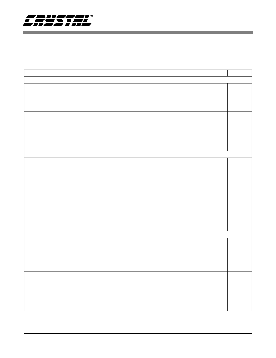
1.0 CHARACTERISTICS/SPECIFICATIONS
ANALOG CHARACTERISTICS
(T
A
= 25 ∞C; Logic "1" = VD = 5 V; VA = 5V; Logic "0" = DGND;
Full-Scale Output Sine Wave, 997 Hz; MCLK = 12.288 MHz; SCLK = 3.072 MHz, Measurement Bandwidth 10 Hz
to 20 kHz, unless otherwise specified. Test load R
L
= 1 k
, C
L
= 10 pF)
Notes: 1. Triangular PDF dithered data.
2. Performance limited by 16-bit quantization noise.
Parameter
Symbol
Min
Typ
Max
Unit
Dynamic Performance - Single Speed Mode - Fs equal to 48 kHz
Dynamic Range
(Note 1)
24-Bit
unweighted
A-Weighted
16-Bit
unweighted
(Note 2)
A-Weighted
TBD
TBD
-
-
117
120
95
98
-
-
-
-
dB
dB
dB
dB
Total Harmonic Distortion + Noise
(Note 1)
24-Bit
0 dB
-20 dB
-60 dB
16-Bit
0 dB
(Note 2)
-20 dB
-60 dB
THD+N
-
-
-
-
-
-
-100
-97
-57
-95
-75
-35
TBD
TBD
TBD
-
-
-
dB
dB
dB
dB
dB
dB
Dynamic Performance - Double Speed Mode - Fs equal to 96 kHz
Dynamic Range
(Note 1)
24-Bit
unweighted
A-Weighted
40 kHz bandwidth
unweighted
16-Bit
unweighted
(Note 2)
A-Weighted
TBD
TBD
TBD
-
-
117
120
114
92
98
-
-
-
-
-
dB
dB
dB
dB
dB
Total Harmonic Distortion + Noise
(Note 1)
24-Bit
0 dB
-20 dB
-60 dB
16-Bit
0 dB
(Note 2)
-20 dB
-60 dB
THD+N
-
-
-
-
-
-
-100
-97
-57
-95
-75
-35
TBD
TBD
TBD
-
-
-
dB
dB
dB
dB
dB
dB
Dynamic Performance - Quad-Speed Mode - Fs equal to 192 kHz
Dynamic Range
(Note 1)
24-Bit
unweighted
A-Weighted
40 kHz bandwidth
unweighted
16-Bit
unweighted
(Note 2)
A-Weighted
TBD
TBD
TBD
-
-
117
120
114
92
98
-
-
-
-
-
dB
dB
dB
dB
dB
Total Harmonic Distortion + Noise
(Note 1)
24-Bit
0 dB
-20 dB
-60 dB
16-Bit
0 dB
(Note 2)
-20 dB
-60 dB
THD+N
-
-
-
-
-
-
-100
-97
-57
-95
-75
-35
TBD
TBD
TBD
-
-
-
dB
dB
dB
dB
dB
dB

CS4396
DS288PP1
5
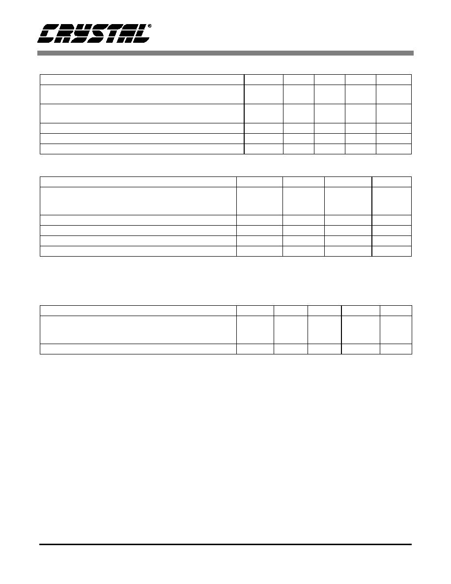
ANALOG CHARACTERISTICS
(Continued)
Notes: 3. Valid with the recommended capacitor values on FILT+ and CMOUT as shown in Figure 1. Increasing
the capacitance will also increase the PSRR.
Parameter
Symbol
VD = 3 V
VD = 5 V
Unit
Power Supplies
Min
Typ
Max Min
Typ
Max
Supply Current
normal operation
VA = 5 V
normal operation
power-down state
I
A
I
D
I
D
+ I
A
-
-
-
20
TBD
60
TBD
TBD
-
-
-
-
20
TBD
30
TBD
TBD
-
mA
mA
µ
A
Power Dissipation normal operation
VA = 5 V
power-down
-
-
TBD
0.3
TBD
-
-
-
TBD
0.3
TBD
-
mW
mW
Power Supply Rejection Ratio (1 kHz)
(Note 3)
(120 Hz)
PSRR
-
-
60
40
-
-
-
-
60
40
-
-
dB
dB
Parameter
Symbol
Min
Typ
Max
Unit
Analog Output
Full Scale Differential Output Voltage
TBD
1.4VREF
TBD
Vpp
Common Mode Voltage
-
0.5VREF
-
VDC
Interchannel Gain Mismatch
-
0.1
-
dB
Gain Drift
-
100
-
ppm/∞C
Differential DC Offset
-
2.0
TBD
mV
AC-Load Resistance
R
L
1
-
-
k
Load Capacitance
C
L
-
-
100
pF
Interchannel Isolation
(1 kHz)
-
90
-
dB

CS4396
6
DS288PP1
ANALOG CHARACTERISTICS
(Continued)
Notes: 4. Response is clock dependent and will scale with Fs. Note that the response plots (Figures 7-18) have
been normalized to Fs and can be de-normalized by multiplying the X-axis scale by Fs.
5. For Single-Speed Mode, the Measurement Bandwidth is 0.5465 Fs to 1.4 Fs.
For Double-Speed Mode, the Measurement Bandwidth is 0.570 Fs to 1.4 Fs.
For Quad-Speed Mode, the Measurement Bandwidth is 0.635 Fs to 1.3 Fs.
6. Group Delay for Fs=48 kHz 37/48 kHz=770
µ
s
7. De-emphasis is available only in Single Speed Mode.
Parameter
Symbol
Min
Typ
Max
Unit
Combined Digital and On-chip Analog Filter Response - Single Speed Mode
Passband
(Note 4)
to -0.1 dB corner
to -3 dB corner
-
-
-
-
0.470
0.492
Fs
Fs
Frequency Response 10 Hz to 20 kHz
-.020
-
+0.015
dB
Passband Ripple
-
-
±0.0001
dB
StopBand
.5465
-
-
Fs
StopBand Attenuation
(Note 5)
102
-
-
dB
Group Delay
(Note 6)
tgd
-
37/Fs
-
s
De-emphasis Error
(Note 7)
Fs = 32 kHz
(Relative to 1 kHz)
Fs = 44.1 kHz
Fs = 48 kHz
-
-
-
-
-
-
±0.10
±0.10
±0.13
dB
dB
dB
Combined Digital and On-chip Analog Filter Response - Double Speed Mode
Passband
(Note 4)
to -0.1 dB corner
to -3 dB corner
0
0
-
-
0.448
0.486
Fs
Fs
Frequency Response 10 Hz to 20 kHz
-0.017
-
0.035
dB
Passband Ripple
-
-
±0.0008
dB
StopBand
.570
-
-
Fs
StopBand Attenuation
(Note 5)
82
-
-
dB
Group Delay
tgd
-
20/Fs
-
s
Combined Digital and On-chip Analog Filter Response - Quad-Speed Mode
Passband
(Note 4)
to -0.1 dB corner
to -3 dB corner
-
-
-
-
0.385
0.472
Fs
Fs
Frequency Response 10 Hz to 20 kHz
0
-
+0.015
dB
Passband Ripple
-
-
±0.00065
dB
StopBand
0.635
-
-
Fs
StopBand Attenuation
(Note 5)
83
-
-
dB
Group Delay
tgd
-
11/Fs
-
s
CS4396
DS288PP1
7
DIGITAL CHARACTERISTICS
(T
A
= 25∞C; VD = 3.0V - 5.25V)
ABSOLUTE MAXIMUM RATINGS
(AGND = 0 V, all voltages with respect to ground.)
WARNING: Operation at or beyond these limits may result in permanent damage to the device. Normal operation
is not guaranteed at these extremes.
RECOMMENDED OPERATING CONDITIONS
(DGND = 0V; all voltages with respect to ground)
Parameters
Symbol Min Typ
Max
Units
High-Level Input Voltage
VD = 5 V
VD = 3 V
V
IH
2.0
2.0
-
-
-
-
V
V
Low-Level Input Voltage
VD = 5 V
VD = 3 V
V
IL
-
-
-
-
0.8
0.8
V
V
Input Leakage Current
I
in
-
-
±10
µ
A
Input Capacitance
-
8
-
pF
Maximum MUTEC Drive Current
-
3
-
mA
Parameter
Symbol Min
Max
Unit
DC Power Supply: Positive Analog
Positive Digital
Reference Voltage
VA
VD
VREF
-0.3
-0.3
-0.3
6.0
6.0
VA
V
V
V
Input Current, Any Pin Except Supplies
I
in
-
±10
mA
Digital Input Voltage
V
IND
-0.3
(VD)+0.4
V
Ambient Operating Temperature (power applied)
T
A
-55
125
∞C
Storage Temperature
T
stg
-65
150
∞C
Parameter
Symbol Min Typ
Max
Unit
DC Power Supply: Positive Digital
Positive Analog
Reference Voltage
VD
VA
VREF
3.0
4.75
TBD
3.3
5.0
5.0
5.25
5.25
VA
V
V
V
Specified Temperature Range
T
A
-10
-
70
∞C
CS4396
8
DS288PP1
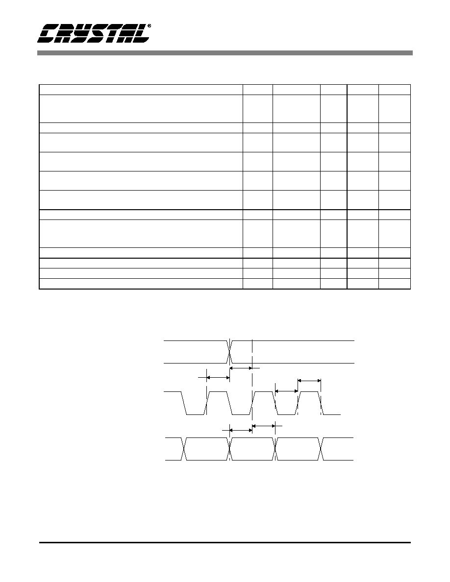
SWITCHING CHARACTERISTICS
(T
A
= -10 to 70∞C; Logic 0 = AGND = DGND; Logic
1 = VD = 5.25 to 3.0 Volts; C
L
= 20 pF)
Parameter
Symbol Min Typ
Max
Unit
Input Sample Rate (Single-speed mode)
(Double-speed mode)
(Quad-speed mode)
Fs
Fs
Fs
16
50
100
-
-
-
50
100
200
kHz
kHz
kHz
LRCK Duty Cycle
45
50
55
%
MCLK Frequency
(Single-speed 256 Fs,
Double speed 128 Fs or Quad-speed 64 Fs)
4.096
-
12.8
MHz
MCLK Frequency
(Single-speed 384 Fs,
Double speed 192 Fs or Quad-speed, 96 Fs
6.144
-
19.2
MHz
MCLK Frequency
(Single-speed 512 Fs,
Double speed 256 Fs or Quad-speed, 128 Fs
8.192
-
25.6
MHz
MCLK Frequency
(Single-speed 768 Fs,
Double speed 384 Fs or Quad-speed, 192 Fs
12.288
-
38.4
MHz
MCLK Duty Cycle
40
50
60
%
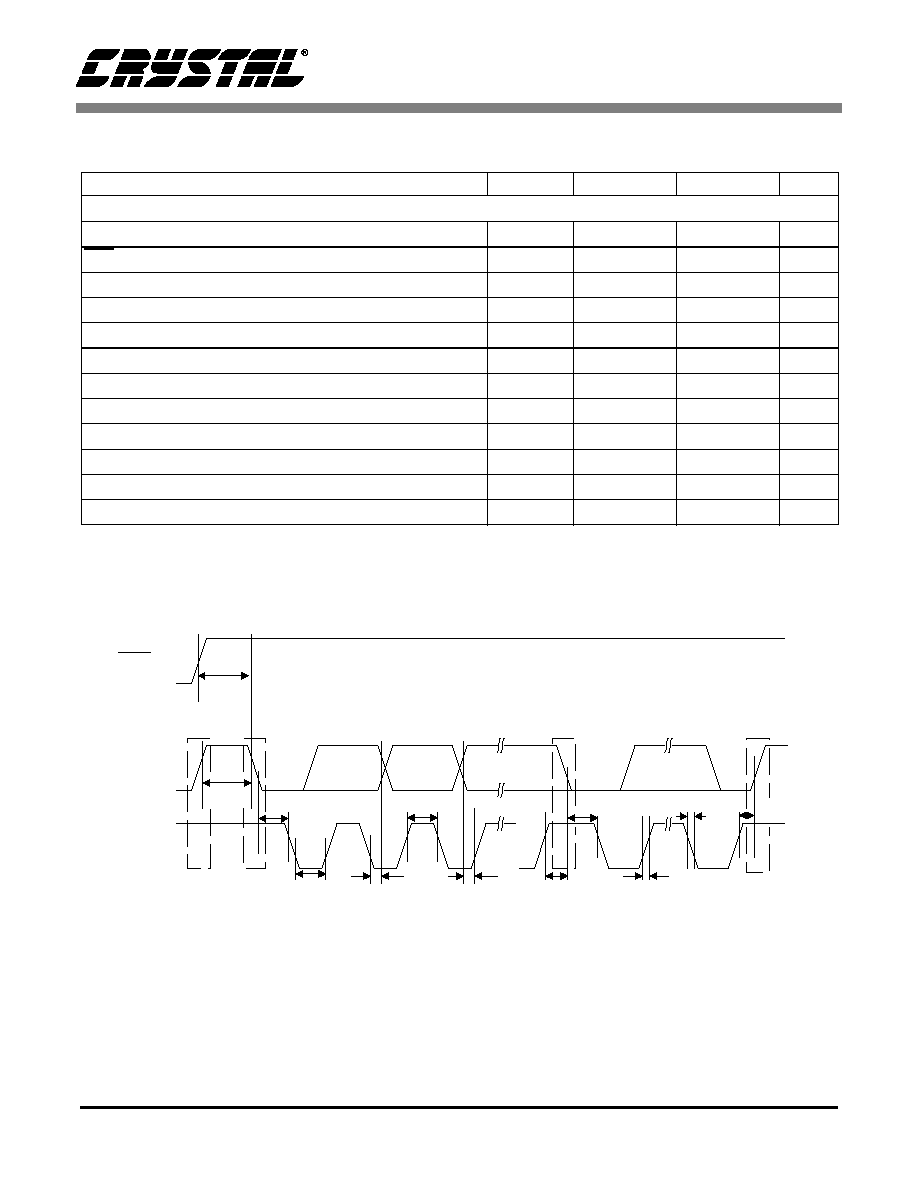
SCLK Frequency (Single-speed mode)
(Double-speed mode)
(Quad-speed mode)
-
-
-
-
-
-
256◊Fs
128◊Fs
64◊Fs
Hz
Hz
Hz
SCLK rising to LRCK edge delay
t
slrd
20
-
-
ns
SCLK rising to LRCK edge setup time
t
slrs
20
-
-
ns
SDATA valid to SCLK rising setup time
t
sdlrs
20
-
-
ns
SCLK rising to SDATA hold time
t
sdh
20
-
-
ns
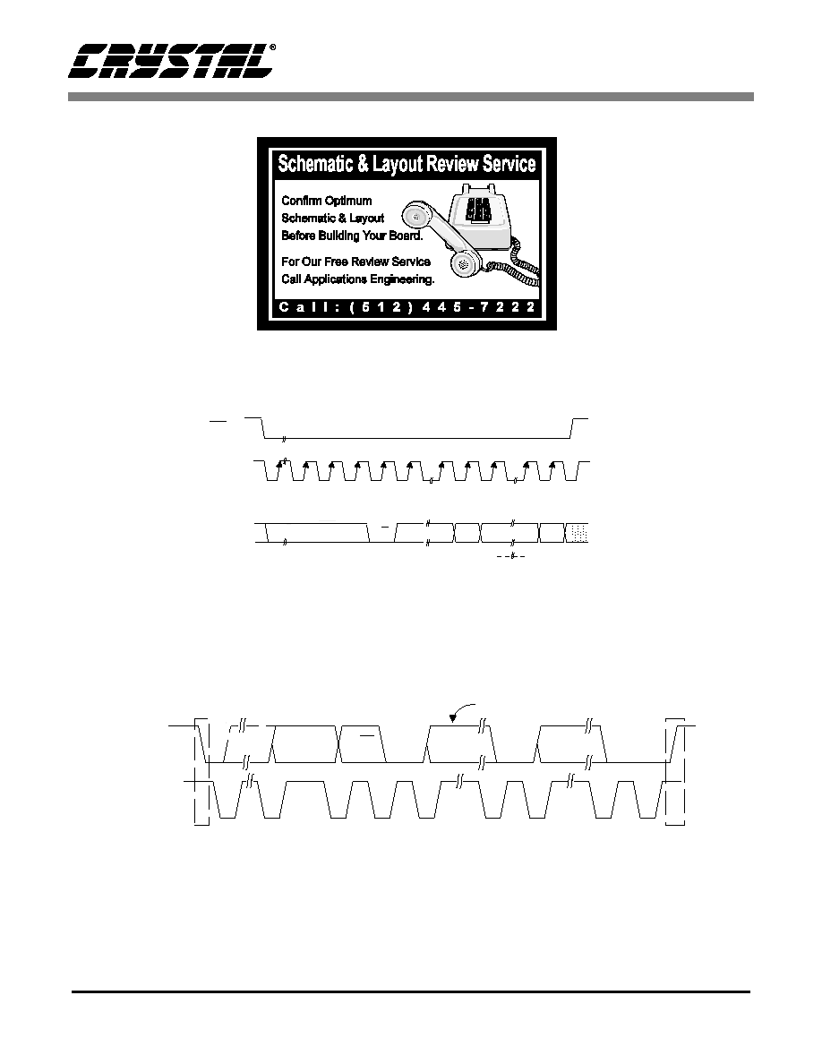
sclkh
t
slrs
t
slrd
t
sdlrs
t
sdh
t
sclkl
t
SDATA
SCLK
LRCK
Figure 1. Serial Audio Input Timing
CS4396
DS288PP1
9
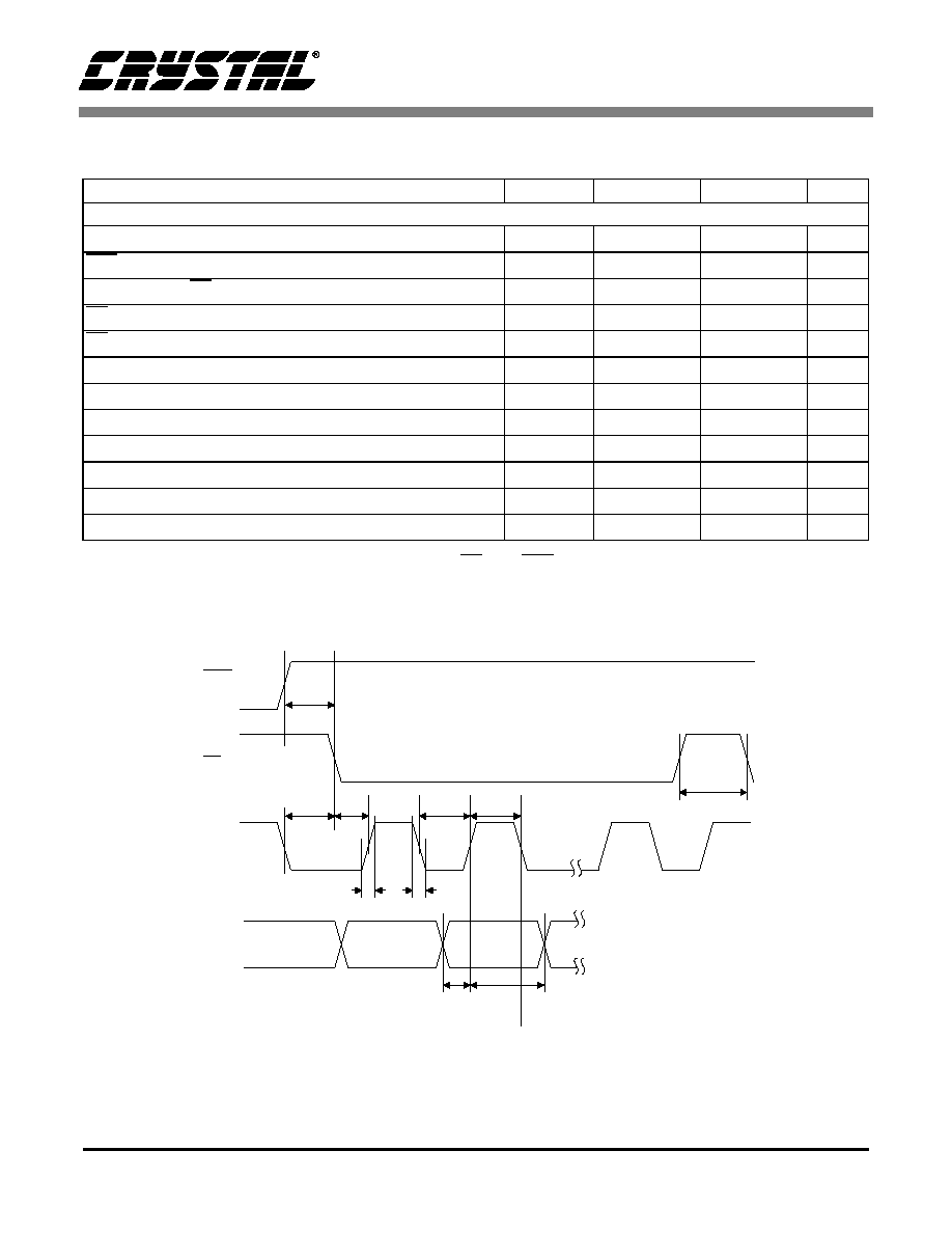
SWITCHING CHARACTERISTICS - CONTROL PORT
(T
A
= 25 ∞C; VD = 5.25 V to 3.0 Volts; Inputs: logic 0 = AGND, logic 1 = VD, C
L
= 30 pF)
Notes: 8. Data must be held for sufficient time to bridge the 300 ns transition time of SCL.
Parameter
Symbol
Min
Max
Unit
I
2
C
Æ
Mode
SCL Clock Frequency
f
scl
-
100
KHz
RST Rising Edge to Start
t
irs
500
-
ns
Bus Free Time Between Transmissions
t
buf
4.7
-
µs
Start Condition Hold Time (prior to first clock pulse)
t
hdst
4.0
-
µs
Clock Low time
t
low
4.7
-
µs
Clock High Time
t
high
4.0
-
µs
Setup Time for Repeated Start Condition
t
sust
4.7
-
µs
SDA Hold Time from SCL Falling
(Note 8)
t
hdd
0
-
µs
SDA Setup time to SCL Rising
t
sud
250
-
ns
Rise Time of Both SDA and SCL Lines
t
r
-
1
µs
Fall Time of Both SDA and SCL Lines
t
f
-
300
ns
Setup Time for Stop Condition
t
susp
4.7
-
µs
t
buf
t
hdst
t
hdst
t
low
t r
t f
t
hdd
t
high
t sud
t sust
t susp
Stop
Start
Start
Stop
Repeated
SDA
SCL
t
irs
RST
Figure 2. I
2
C Control Port Timing
CS4396
10
DS288PP1
SWITCHING CHARACTERISTICS - CONTROL PORT
(T
A
= 25 ∞C; VD = 5.25 V to 3.0 Volts; Inputs: logic 0 = AGND, logic 1 = VD, C
L
= 30 pF)
Notes: 9. t
spi
only needed before first falling edge of CS after RST rising edge. t
spi
= 0 at all other times.
10. Data must be held for sufficient time to bridge the transition time of CCLK.
11. For F
SCK
< 1 MHz
Parameter
Symbol
Min
Max
Unit
SPI Mode
CCLK Clock Frequency
f
sclk
-
6
MHz
RST Rising Edge to CS Falling
t
srs
500
-
ns
CCLK Edge to CS Falling
(Note 9)
t
spi
500
-
ns
CS High Time Between Transmissions
t
csh
1.0
-
µs
CS Falling to CCLK Edge
t
css
20
-
ns
CCLK Low Time
t
scl
66
-
ns
CCLK High Time
t
sch
66
-
ns
CDIN to CCLK Rising Setup Time
t
dsu
40
-
ns
CCLK Rising to DATA Hold Time
(Note 10)
t
dh
15
-
ns
Rise Time of CCLK and CDIN
(Note 11)
t
r2
-
100
ns
Fall Time of CCLK and CDIN
(Note 11)
t
f2
-
100
ns
CCLK Falling to CDOUT valid
t
ov
45
ns
t r2
t f2
t dsu t dh
t sch
t scl
CS
CCLK
CDIN
t css
t csh
t spi
t srs
RST
Figure 3. SPI Control Port Timing
CS4396
DS288PP1
11
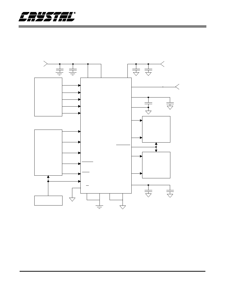
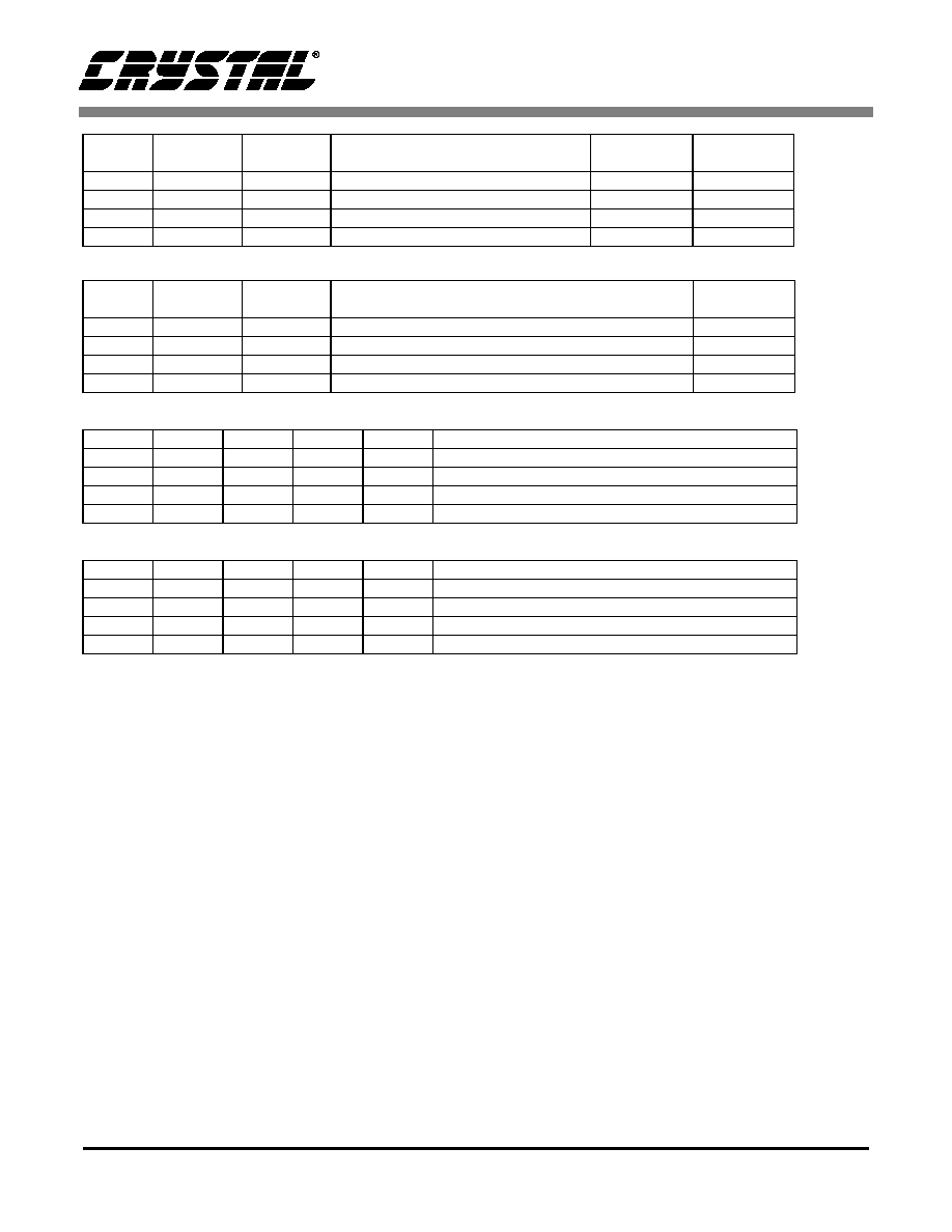
2.0 TYPICAL CONNECTION DIAGRAM
SCLK
Audio
Data
Processor
External Clock
MCLK
AGND
AOUTR+
CS4396
SDATA
VA
AOUTR-
+5V
Analog
0.1
µ
F
+ 1
µ
F
Mode
Select
M1
M0
AOUTL-
AOUTL+
DGND
VD
MUTE
Analog
Conditioning
Analog
Conditioning
7
22
24
23
19
20
18
9
1
15
13
11
12
4
14
5
M2
LRCK
1.0
µ
F
+
RST
10
M3
M4
2
3
16
25
0.1 µf
10 µf
0.1 µf
10 µf
26
27
VREF
FILT+
FILT-
+5V
Analog
28
6
21
MUTEC
0.1 µf
8
17
+
+
CMOUT
C/H
Figure 4. Typical Connection Diagram - Hardware Mode (Control Port Mode)
CS4396
12
DS288PP1
3.0 REGISTER DESCRIPTION
3.1 DIFFERENTIAL DC OFFSET CALIBRATION
Mode Control Register (address 01h)
Access:
R/W in I
2
C and SPI.
Default:
0 - Disabled
Function:
Enabling this function will initiate a calibration to minimize the differential DC offset. This function will be
automatically reset following completion of the calibration sequence.
3.2 SOFT MUTE
Mode Control Register (address 01h)
Access:
R/W in I
2
C and SPI.
Default:
0 - Enabled
Function:
The analog outputs will ramp to a muted state when enabled. The ramp requires 1152 left/right clock cy-
cles in Single Speed, 2304 cycles in Double Speed and 4608 cycles in Quad Speed mode. The bias volt-
age on the outputs will be retained and MUTEC will go low at the completion of the ramp period.
The analog outputs will ramp to a normal state when this function transitions from the enabled to disabled
state. The ramp requires 1152 left/right clock cycles in Single Speed, 2304 cycles in Double Speed and
4608 cycles in Quad Speed mode. The MUTEC will go high immediately on disabling of MUTE.
7
6
5
4
3
2
1
0
CAL
MUTE
M4
M3
M2
M1
M0
PDN
CAL
MODE
0
Disabled : CAL complete
1
Enabled : CAL initiated
Table 1.
7
6
5
4
3
2
1
0
CAL
MUTE
M4
M3
M2
M1
M0
PDN
MUTE
MODE
0
Enabled
1
Disabled
Table 2.
CS4396
DS288PP1
13
3.3 MODE SELECT
Mode Control Register (address 01h)
Access:
R/W in I
2
C and SPI.
Default:
00000
Function:
The Mode Select pins determine the operational mode of the device as detailed in Tables 7-10. The op-
tions include:
Selection of the Digital Interface Format which determines the required relationship between the
Left/Right clock, serial clock and serial data as detailed in Figures 20-23
Selection of the standard 15
µ
s/50
µ
s digital de-emphasis filter response, Figure 28, which requires re-
configuration of the digital filter to maintain the proper filter response for 32, 44.1 or 48 kHz sample rates.
Selection of the appropriate clocking mode to match the input sample rates.
3.4 POWER DOWN
Mode Control Register (address 01h)
Access:
R/W in I
2
C and SPI.
Default:
1 - Powered Down
Function:
The analog and digital sections will be placed into a power-down mode when this function is enabled. This
bit must be cleared to resume normal operation.
7
6
5
4
3
2
1
0
CAL
MUTE
M4
M3
M2
M1
M0
PDN
7
6
5
4
3
2
1
0
CAL
MUTE
M4
M3
M2
M1
M0
PDN
PDN
MODE
0
Disabled
1
Enabled
Table 3.

CS4396
14
DS288PP1
4.0 PIN DESCRIPTION
Reset - RST
Pin 1, Input
Function:
The device enters a low power mode and all internal state machines registers are reset when low. When
high, the device will be in a normal operation mode .
Digital Ground - DGND
Pins 6 and 9, Inputs
Function:
Digital ground reference.
Digital Power - VD
Pins 7 and 8, Input
Function:
Digital power supply. Typically 5.0 to 3.0 VDC.
Master Clock - MCLK
Pin 10, Input
Function:
The master clock frequency must be either 256x, 384x, 512x or 768x the input sample rate in Single
Speed Mode; either 128x, 192x 256x or 384x the input sample rate in Double Speed Mode; or 64x, 96x
128x or 192x the input sample rate in Quad Speed Mode. Tables 4-6 illustrate the standard audio sample
rates and the required master clock frequencies.
RST
DESCRIPTION
0
Enabled
1
Normal operation mode
1
2
3
4
5
6
7
8
9
10
11
12
5
1
2
6
28
27
26
25
24
23
22
21
20
19
18
17
13
14
16
15
Reset
RST
VREF
Voltage Reference
See Description
M4(AD0/CS)
FILT+
Reference Filter
See Description
M3(AD1/CDIN)
FILT-
Reference Ground
See Description
M2(SCL/CCLK)
CMOUT
Common ModeS Voltage
See Description M0(SDA/CDOUT)
AOUTL-
Differential Output
Digital Ground
DGND
AOUTL+
Differential Output
Digital Power
VD
VA
Analog Power
Digital Power
VD
AGND
Analog Ground
Digital Ground
DGND
AOUTR+
Differential Output
Master Clock
MCLK
AOUTR-
Differential Output
Serial Clock
SCLK
AGND
Analog Ground
Left/Right Clock
LRCK
MUTEC
Mute Control
Serial Data
SDATA
C/H
Control port/Hardware select
See Description
M1
MUTE
Soft Mute

CS4396
DS288PP1
15
Serial Clock - SCLK
Pin 11, Input
Function:
Clocks individual bits of serial data into the SDATA pin. The required relationship between the Left/Right
clock, serial clock and serial data is defined by either the Mode Control Byte in Control Port Mode or the
M0 - M4 pins in Hardware Mode. The options are detailed in Figures 20-23
Left/Right Clock - LRCK
Pin 12, Input
Function:
The Left/Right clock determines which channel is currently being input on the serial audio data input,
SDATA. The frequency of the Left/Right clock must be at the input sample rate. Audio samples in
Left/Right sample pairs will be simultaneously output from the digital-to-analog converter whereas
Right/Left pairs will exhibit a one sample period difference. The required relationship between the
Left/Right clock, serial clock and serial data is defined by the Mode Control Byte and the options are de-
tailed in Figures 20-23
Serial Audio Data - SDATA
Pin 13, Input
Function:
Two's complement MSB-first serial data is input on this pin. The data is clocked into SDATA via the serial
clock and the channel is determined by the Left/Right clock. The required relationship between the
Left/Right clock, serial clock and serial data is defined by the Mode Control Byte and the options are de-
tailed inin Figures 20-23
Soft Mute - MUTE
Pin 15, Input
Function:
The analog outputs will ramp to a muted state when enabled. The ramp requires 1152 left/right clock cy-
Sample Rate
(kHz)
MCLK (MHz)
256x
384x
512x
768x
32
8.1920
12.2880
16.3840
24.5760
44.1
11.2896
16.9344
22.5792
33.8688
48
12.2880
18.4320
24.5760
36.8640
Table 4. Single Speed (16 to 50 kHz sample rates) Common Clock Frequencies
Sample Rate
(kHz)
MCLK (MHz)
128x
192x
256x
384x
64
8.1920
12.2880
16.3840
24.5760
88.2
11.2896
16.9344
22.5792
33.8688
96
12.2880
18.4320
24.5760
36.8640
Table 5. Double Speed (50 to 100 kHz sample rates) Common Clock Frequencies
Sample Rate
(kHz)
MCLK (MHz)
64x
96x
128x
192x
176.4
11.2896
16.9344
22.5792
33.8688
192
12.2880
18.4320
24.5760
36.8640
Table 6. Quad Speed (100 to 200 kHz sample rates) Common Clock Frequencies

CS4396
16
DS288PP1
cles in Single Speed, 2304 cycles in Double Speed and 4608 cycles in Quad Speed mode. The bias volt-
age on the outputs will be retained and MUTEC will go active at the completion of the ramp period.
The analog outputs will ramp to a normal state when this function transitions from the enabled to disabled
state. The ramp requires 1152 left/right clock cycles in Single Speed, 2304 cycles in Double Speed and
4608 cycles in Quad Speed mode. The MUTEC will release immediately on setting MUTE = 1.
The converter analog outputs will mute when enabled. The bias voltage on the outputs will be retained
and MUTEC will go active during the mute period.
Control Port / Hardware Mode Select - C/H
Pin 16, Input
Function:
Determines if the device will operate in either the Hardware Mode or Control Port Mode.
Mute Control - MUTEC
Pin 17, Output
Function:
The Mute Control pin goes low during power-up initialization, reset, muting, master clock to left/right clock
frequency ratio is incorrect or power-down. This pin is intended to be used as a control for an external mute
circuit to prevent the clicks and pops that can occur in any single supply system. Use of Mute Control is not
mandatory but recommended for designs requiring the absolute minimum in extraneous clicks and pops.
Analog Ground - AGND
Pins 18 and 21, Inputs
Function:
Analog ground reference.
Differential Analog Outpus - AOUTR- , AOUTR+ and AOUTL- , AOUTL+
Pins 19, 20, 23 and 24, Outputs
Function:
The full scale differential analog output level is specified in the Analog Characteristics specifications table.
Analog Power - VA
Pin 22, Input
Function:
Power for the analog and reference circuits. Typically 5VDC.
Mute
DESCRIPTION
0
Enabled
1
Normal operation mode
C/H
DESCRIPTION
0
Hardware Mode Enabled
1
Control Port Mode Enabled

CS4396
DS288PP1
17
Common Mode Voltage - CMOUT
Pin 25, Output
Function:
Filter connection for internal bias voltage, typically 50% of VREF. Capacitors must be connected from
CMOUT to analog ground, as shown in Figure 4. CMOUT has a typical source impedence of 25 k
and
any current drawn from this pin will alter device performance
Reference Ground - FILT-
Pin 26, Input
Function:
Ground reference for the internal sampling circuits. Must be connected to analog ground.
Reference Filter - FILT+
Pin 27, Output
Function:
Positive reference for internal sampling circuits. External capacitors are required from FILT+ to analog
ground, as shown in Figure 4. The recommended values will typically provide 60 dB of PSRR at 1 kHz
and 40 dB of PSRR at 120 Hz. FILT+ is not intended to supply external current.
Voltage Reference Input- VREF
Pin 28, Input
Function:
Analog voltage reference. Typically 5VDC.
HARDWARE MODE
Mode Select - M0, M1, M2, M3, M4
Pins 2, 3, 4, 5 and 14, Inputs
Function:
The Mode Select pins determine the operational mode of the device as detailed in Tables 7-10. The op-
tions include;
Selection of the Digital Interface Format which determines the required relationship between the
Left/Right clock, serial clock and serial data as detailed in Figures 20-23
Selection of the standard 15
µ
s/50
µ
s digital de-emphasis filter response, Figure 28, which requires re-
configuration of the digital filter to maintain the proper filter response for 32, 44.1 or 48 kHz sample rates.
Selection of the appropriate clocking mode to match the input sample rates.
CONTROL PORT MODE
Address Bit 0 / Chip Select - AD0 / CS
Pin 2, Input
Function:
In I
2
C mode, AD0 is a chip address bit. CS is used to enable the control port interface in SPI mode. The
device will enter the SPI mode at anytime a high to low transition is detected on this pin. Once the device
has entered the SPI mode, it will remain until either the part is reset or undergoes a power-down cycle.

CS4396
18
DS288PP1
Address Bit 1 / Control Data Input - AD1/CDIN
Pin 3, Input
Function:
In I
2
C mode, AD1 is a chip address bit. CDIN is the control data input line for the control port interface in
SPI mode.
Serial Control Interface Clock - SCL/CCLK
Pin 4, Input
Function:
In I
2
C mode, SCL clocks the serial control data into or from SDA/CDOUT.
In SPI mode, CCLK clocks the serial data into AD1/CDIN and out of SDA/CDOUT.
Serial Control Data I/O - SDA/CDOUT
Pin 5, Input/Output
Function:
In I
2
C mode, SDA is a data input/output. CDOUT is the control data output for the control port interface in
SPI mode.
M1 - Mode Select
Pin 14, Input
Function:
This pin is not used in Control Port Mode and must be terminated to ground.

CS4396
DS288PP1
19
5.0 APPLICATIONS
5.1 Recommended Power-up Sequence
1. Hold RST low until the power supplies, master, and left/right clocks are stable.
2. Bring RST high.
CS4396
20
DS288PP1
6.0 CONTROL PORT INTERFACE
The control port is used to load all the internal settings of the CS4396. The operation of the control port
may be completely asynchronous to the audio sample rate. However, to avoid potential interference prob-
lems, the control port pins should remain static if no operation is required.
The control port has 2 modes: SPI and I
2
C, with the CS4396 operating as a slave device in both modes. If
I
2
C operation is desired, AD0/CS should be tied to VD or DGND. If the CS4396 ever detects a high to low
transition on AD0/CS after power-up, SPI mode will be selected.
6.1 SPI Mode
In SPI mode, CS is the CS4396 chip select signal, CCLK is the control port bit clock, CDIN is the input
data line from the microcontroller, CDOUT is the data output and the chip address is 0010000. The data
is clocked on the rising edge of CCLK.
Figure 5 shows the operation of the control port in SPI mode. To write to a register, bring CS low. The first
7 bits on CDIN form the chip address, and must be 0010000. The eighth bit is a read/write indicator (R/W).
The next 8 bits form the Memory Address Pointer (MAP), which is set to 01h. The next 8 bits are the data
which will be placed into the register designated by the MAP.
6.2 I
2
C Mode
In I
2
C mode, SDA is a bi-directional data line. Data is clocked into and out of the part by the clock, SCL,
with the clock to data relationship as shown in Figure 2. There is no CS pin. Pins AD0 and AD1 form the
partial chip address and should be tied to VD or DGND as required. The 7-bit address field, which is the
first byte sent to the CS4396, must be 00100(AD1)(AD0) where (AD1) and (AD0) match the setting of the
AD0 and AD1 pins. The eighth bit of the address byte is the R/W bit (high for a read, low for a write). If
the operation is a write, the next byte is the Memory Address Pointer, MAP, which selects the register to
be read or written. The MAP is then followed by the data to be written. If the operation is a read, then the
contents of the register pointed to by the MAP will be output after the chip address.
For more information on I
2
C, please see "The I
2
C-Bus Specification: Version 2.0", listed in the References
section.
Memory Address Pointer (MAP)
INCR (Auto MAP Increment Enable)
MAP0-2 (Memory Address Pointer)
Default = `0'
Default = `001'
0 - Disabled
1 - Enabled
7
6
5
4
3
2
1
0
INCR
Reserved
Reserved
Reserved
Reserved
MAP2
MAP1
MAP0
0
0
0
0
0
0
0
1
CS4396
DS288PP1
21
SDA
SCL
001000
ADDR
AD0
R/W
Start
ACK
DATA
1-8
ACK
DATA
1-8
ACK
Stop
Note: If operation is a write, this byte contains the Memory Address Pointer, MAP.
Note 1
Figure 6. Control Port Timing, I
2
C Mode
MAP
MSB
LSB
DATA
byte 1
byte n
R/W
MAP = Memory Address Pointer = 0
ADDRESS
CHIP
CDIN
CCLK
CS
0010000
Figure 5. Control Port Timing, SPI mode
CS4396
22
DS288PP1
M4
M1
(DIF1)
M0
(DIF0)
DESCRIPTION
FORMAT
FIGURE
0
0
0
Left Justified, up to 24-bit data
0
20
0
0
1
I
2
S, up to 24-bit data
1
21
0
1
0
Right Justified, 16-bit Data
2
22
0
1
1
Right Justified, 24-bit Data
3
23
Table 7. Single Speed (16 to 50 kHz) Digital Interface Format Options
M4
M3
(DEM1)
M2
(DEM0)
DESCRIPTION
FIGURE
0
0
0
32 kHz De-Emphasis
19
0
0
1
44.1 kHz De-Emphasis
19
0
1
0
48 kHz De-Emphasis
19
0
1
1
De-Emphasis Disabled
-
Table 8. Single Speed (16 to 50 kHz) De-Emphasis Options
M4
M3
M2
M1
M0
DESCRIPTION
1
1
1
0
0
Left Justified up to 24-bit data, Format 0
1
1
1
0
1
I
2
S up to 24-bit data, Format 1
1
1
1
1
0
Right Justified 16-bit data, Format 2
1
1
1
1
1
Right Justified 24-bit data, Format 3
Table 9. Double Speed (50 to 100 kHz) Sample Rate Mode Options
M4
M3
M2
M1
M0
DESCRIPTION
1
1
0
0
0
Left Justified up to 24-bit data, Format 0
1
1
0
0
1
I
2
S up to 24-bit data, Format 1
1
1
0
1
0
Right Justified 16-bit data, Format 2
1
1
0
1
1
Right Justified 24-bit data, Format 3
Table 10. Quad (100 to 200 kHz) Sample Rate Mode Options
CS4396
DS288PP1
23
-160
-140
-120
-100
-80
-60
-40
-20
0
0.45 0.46 0.47 0.48 0.49 0.5 0.51 0.52 0.53 0.54 0.55 0.56 0.57 0.58 0.59 0.6
Frequency (normalized to Fs)
A
m
pl
i
t
ude
dB
0.46 0.48 0.50 0.52 0.54 0.56 0.58 0.6
-160
-140
-120
-100
-80
-60
-40
-20
0
0.45
0.5
0.55
0.6
0.65
0.7
0.75
0.8
0.85
0.9
0.95
1
Frequency (normalized to Fs)
A
m
pl
i
t
ude
dB
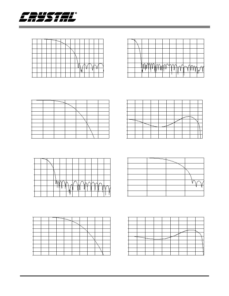
Figure 7. Single-speed Transition Band
Figure 8. Single-speed Stopband Rejection
-10
-9
-8
-7
-6
-5
-4
-3
-2
-1
0
0.45
0.46
0.47
0.48
0.49
0.5
0.51
0.52
Frequency (normalized to Fs)
A
m
pl
i
t
ude
dB
-0.1
-0.08
-0.06
-0.04
-0.02
0
0.02
0.04
0.06
0.08
0.1
0
0.05
0.1
0.15
0.2
0.25
0.3
0.35
0.4
0.45
Frequency (normalized to Fs)
A
m
pl
i
t
ude
dB
Figure 9. Single-speed Transition Band
Figure 10. Single-speed Frequency Response
-140
-120
-100
-80
-60
-40
-20
0
0.4
0.45
0.5
0.55
0.6
0.65
0.7
0.75
0.8
0.85
0.9
0.95
1
Frequency (normalized to Fs)
A
m
pl
i
t
ude
dB
-140
-120
-100
-80
-60
-40
-20
0
0.4
0.45
0.5
0.55
0.6
Frequency (normalized to Fs)
A
m
pl
i
t
ude
dB
Figure 11. Double-speed Stopband
Figure 12. Double-speed Transition Band
-10
-9
-8
-7
-6
-5
-4
-3
-2
-1
0
0.42
0.43
0.44
0.45
0.46
0.47
0.48
0.49
0.5
0.51
0.52
Frequency (normalized to Fs)
A
m
pl
i
t
ude
dB
-0.1
-0.08
-0.06
-0.04
-0.02
0
0.02
0.04
0.06
0.08
0.1
0
0.05
0.1
0.15
0.2
0.25
0.3
0.35
0.4
0.45
Frequency (normalized to Fs)
A
m
pl
i
t
ude
dB
Figure 13. Double-speed Transition Band
Figure 14. Double-speed Frequency Response
CS4396
24
DS288PP1
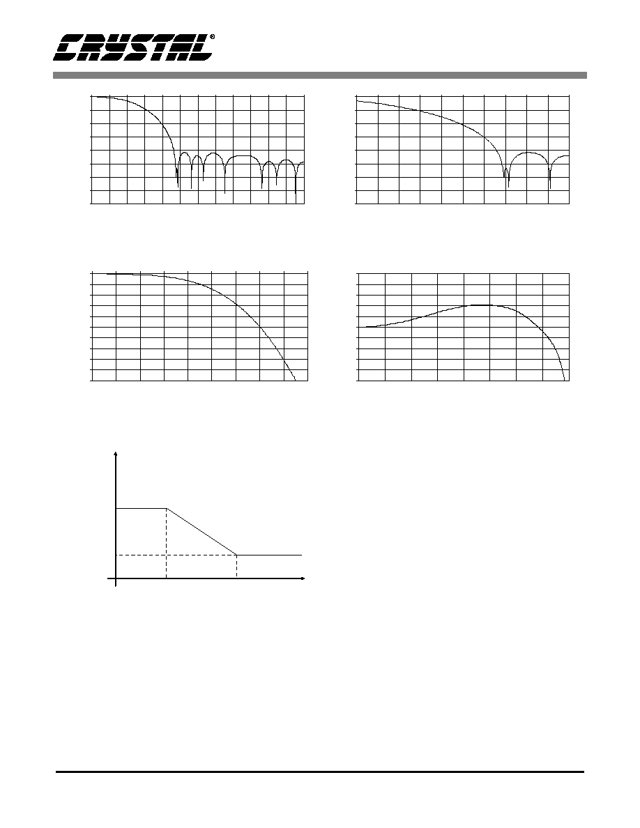
-160
-140
-120
-100
-80
-60
-40
-20
0
0.4
0.45
0.5
0.55
0.6
0.65
0.7
0.75
0.8
0.85
0.9
0.95
1
Frequency (normalized to Fs)
A
m
pl
i
t
ude
dB
-160
-140
-120
-100
-80
-60
-40
-20
0
0.5
0.52
0.54
0.56
0.58
0.6
0.62
0.64
0.66
0.68
0.7
Frequency (normalized to Fs)
A
m
pl
i
t
ude
dB
Figure 15. Quad-speed Stopband Rejection
Figure 16. Quad-speed Transition Band
-0.1
-0.08
-0.06
-0.04
-0.02
0
0.02
0.04
0.06
0.08
0.1
0
0.05
0.1
0.15
0.2
0.25
0.3
0.35
0.4
Frequency (normalized to Fs)
A
m
pl
i
t
ude
dB
-10
-9
-8
-7
-6
-5
-4
-3
-2
-1
0
0.35
0.37
0.39
0.41
0.43
0.45
0.47
0.49
0.51
0.53
Frequency (normalized to Fs)
A
m
pl
i
t
ude
dB
Figure 17. Quad-speed Transition Band
Figure 18. Quad-speed Frequency Response
Figure 19. De-Emphasis Curve
Gain
dB
-10dB
0dB
Frequency
T2 = 15 µs
T1=50 µs
F1
F2
3.183 kHz
10.61 kHz
CS4396
DS288PP1
25
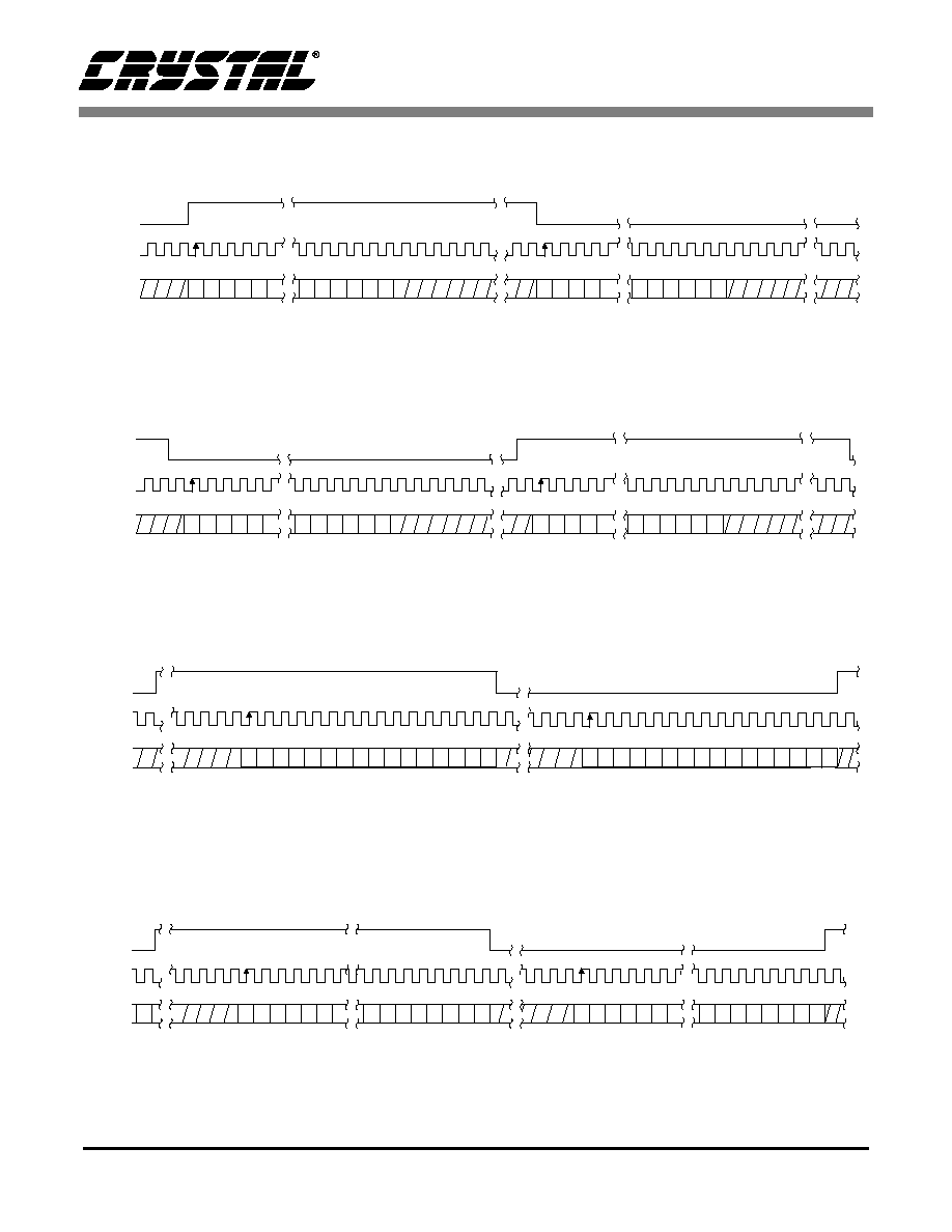
LRCK
SCLK
Left Channel
Right Channel
SDATA
+3 +2 +1 LSB
+5 +4
MSB -1 -2 -3 -4 -5
+3 +2 +1 LSB
+5 +4
MSB -1 -2 -3 -4
Figure 20. Format 0, Left Justified
LRCK
SCLK
Left Channel
Right Channel
SDATA
+3 +2 +1 LSB
+5 +4
MSB -1 -2 -3 -4 -5
+3 +2 +1 LSB
+5 +4
MSB -1 -2 -3 -4
Figure 21. Format 1, I
2
S
LRCK
SCLK
Left Channel
Right Channel
SDATA
6
5
4
3
2
1
0
9
8
7
15 14 13 12 11 10
6
5
4
3
2
1
0
9
8
7
15 14 13 12 11 10
32 clocks
Figure 22. Format 2, Right Justified, 16-Bit Data
LRCK
SCLK
Left Channel
SDATA
6
5
4
3
2
1
0
7
23 22 21 20 19 18
6
5
4
3
2
1
0
7
23 22 21 20 19 18
32 clocks
0
Right Channel
Figure 23. Format 3, Right Justified, 24-Bit Data

CS4396
26
DS288PP1
7.0 PARAMETER DEFINITIONS
Total Harmonic Distortion + Noise (THD+N)
The ratio of the rms value of the signal to the rms sum of all other spectral components over the specified
bandwidth (typically 10Hz to 20kHz), including distortion components. Expressed in decibels.
Dynamic Range
The ratio of the full scale rms value of the signal to the rms sum of all other spectral components over the
specified bandwidth. Dynamic range is a signal-to-noise measurement over the specified bandwidth
made with a -60 dBFS signal. 60 dB is then added to the resulting measurement to refer the measurement
to full scale. This technique ensures that the distortion components are below the noise level and do not
effect the measurement. This measurement technique has been accepted by the Audio Engineering So-
ciety, AES17-1991, and the Electronic Industries Association of Japan, EIAJ CP-307.
Interchannel Isolation
A measure of crosstalk between the left and right channels. Measured for each channel at the converter's
output with all zeros to the input under test and a full-scale signal applied to the other channel. Units in
decibels.
Interchannel Gain Mismatch
The gain difference between left and right channels. Units in decibels.
Gain Error
The deviation from the nominal full scale analog output for a full scale digital input.
Gain Drift
The change in gain value with temperature. Units in ppm/∞C.
8.0 REFERENCES
1) "How to Achieve Optimum Performance from Delta-Sigma A/D & D/A Converters" by Steven Harris.
Paper presented at the 93rd Convention of the Audio Engineering Society, October 1992.
2) CDB4397 Evaluation Board Datasheet
3) "The I
2
C-Bus Specification: Version 2.0" Philips Semiconductors, December 1998.
http://www.semiconductors.philips.com
CS4396
DS288PP1
27
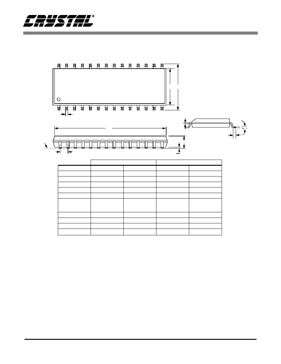
9.0 PACKAGE DIMENSIONS
INCHES
MILLIMETERS
DIM
MIN
MAX
MIN
MAX
A 0.093
0.104
2.35
2.65
A1
0.004
0.012
0.10
0.30
B
0.013
0.020
0.33
0.51
C
0.009
0.013
0.23
0.32
D
0.697
0.713
17.70
18.10
E
0.29G10
1
0.299
7.40
7.60
e
0.040
0.060
1.02
1.52
H
0.394
0.419
10.00
10.65
L
0.016
0.050
0.40
1.27
0∞
8∞
0∞
8∞
JEDEC #: MS-013
28L SOIC (300 MIL BODY) PACKAGE DRAWING
D
H
E
b
A1
A
c
L
SEATING
PLANE
1
e